16-Bit Registered Transceivers
CY74FCT16646T
CY74FCT162646T
SCCS060 - August 1994 - Revised March 2000
Data sheet acquired from Cypress Semiconductor Corporation.
Data sheet modified to remove devices not offered.
Copyright
©
2000, Texas Instruments Incorporated
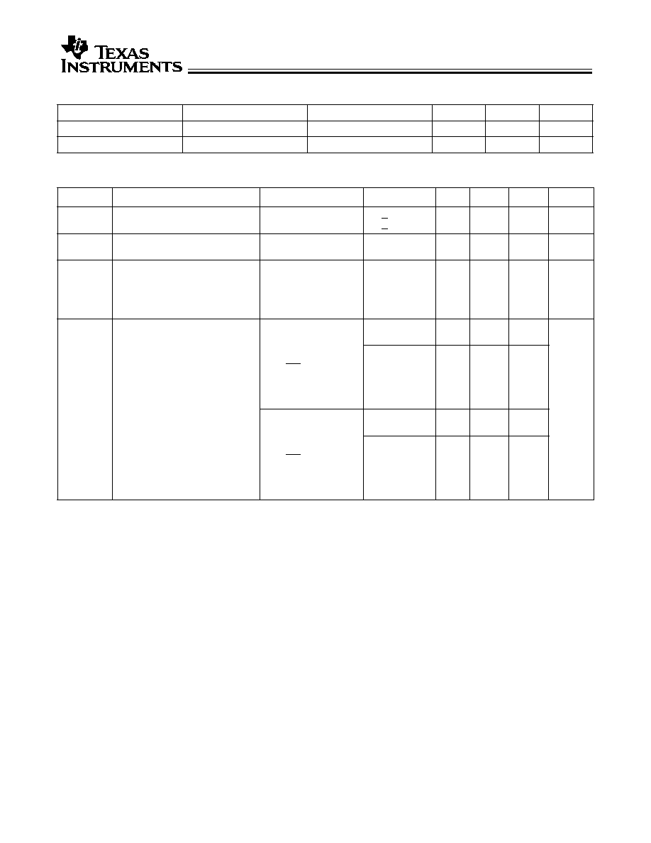
Features
∑ FCT-E speed at 3.8 ns
∑ Power-off disable outputs permits live insertion
∑ Edge-rate control circuitry for significantly improved
noise characteristics
∑ Typical output skew < 250 ps
∑ ESD > 2000V
∑ TSSOP (19.6-mil pitch) and SSOP (25-mil pitch)
packages
∑ Industrial temperature range of
-
40∞C to +85∞C
∑ V
CC
= 5V
±
10%
CY74FCT16646T Features:
∑ 64 mA sink current, 32 mA source current
∑ Typical V
OLP
(ground bounce) <1.0V at V
CC
= 5V,
T
A
= 25∞C
CY74FCT162646T Features:
∑ Balanced 24 mA output drivers
∑ Reduced system switching noise
∑ Typical V
OLP
(ground bounce) <0.6V at V
CC
= 5V,
T
A
= 25∞C
Functional Description
The
CY74FCT16646T
and
CY74FCT162646T
16-bit
transceivers are three-state, D-type registers, and control
circuitry arranged for multiplexed transmission of data directly
from the input bus or from the internal registers. Data on the A
or B bus will be clocked into the registers as the appropriate
clock pin goes to a HIGH logic level. Output Enable (OE) and
direction pins (DIR) are provided to control the transceiver
function. In the transceiver mode, data present at the high
impedance port may be stored in either the A or B register, or
in both. The select controls can multiplex stored and real-time
(transparent mode) data. The direction control determines
which bus will receive data when the Output Enable (OE) is
Active LOW. In the isolation mode (Output Enable (OE) HIGH),
A data may be stored in the B register and/or B data may be
stored in the A register. The output buffers are designed with
a power-off disable feature that allows live insertion of boards.
The
CY74FCT16646T
is
ideally
suited
for
driving
high-capacitance loads and low-impedance backplanes.
The CY74FCT162646T has 24-mA balanced output drivers
with current limiting resistors in the outputs. This reduces the
need for external terminating resistors and provides for
minimal undershoot and reduced ground bounce. The
CY74FCT162646T is ideal for driving transmission lines.
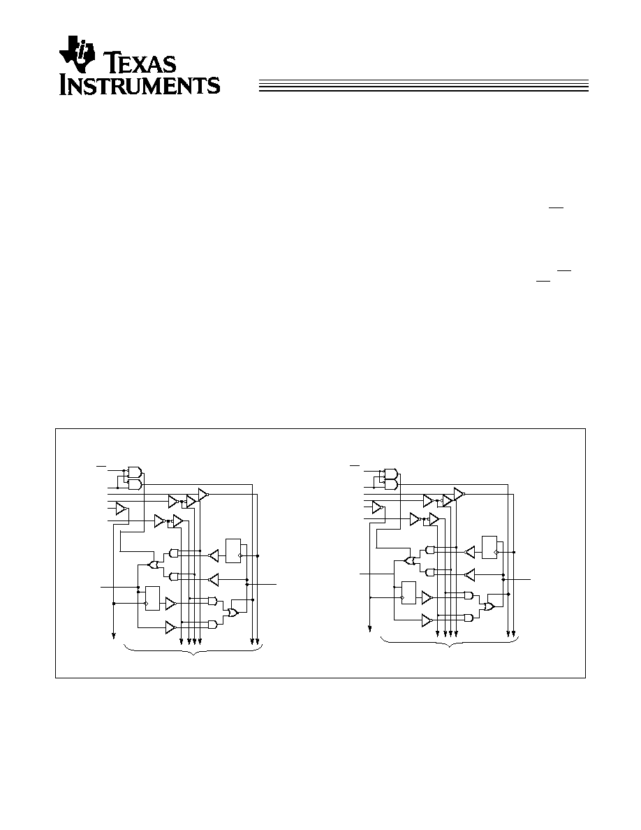
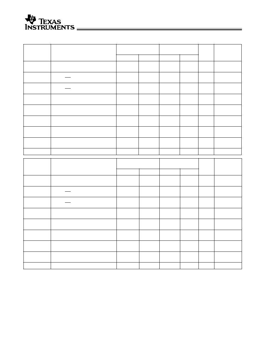
Logic Block Diagrams
FCT16646-1
C
D
1B1
C
D
1A1
TO 7 OTHER CHANNELS
1SAB
1CLKAB
1CLKBA
1DIR
1SBA
1OE
B REG
A REG
C
D
2B1
C
D
2A1
2SAB
2CLKAB
2CLKBA
2DIR
2SBA
2OE
B REG
FCT16646-2
TO 7 OTHER CHANNELS
A REG
CY74FCT16646T
CY74FCT162646T
2
GND
1DIR
SSOP/TSSOP
Top View
1CLKAB
1SAB
1A1
1A2
1CLKBA
1SBA
1B1
1OE
GND
GND
VCC
1A3
VCC
GND
1A4
1A5
1A6
1A7
1A8
2A1
2A2
2A3
2A4
GND
2A5
2A6
VCC
2A7
2A8
2SAB
2CLKAB
1
2
3
4
5
6
7
8
9
10
11
12
13
14
15
16
17
18
19
20
21
22
23
24
25
26
27
28
56
55
54
53
52
51
50
49
48
47
46
45
44
43
42
41
40
39
38
37
36
35
34
33
32
31
30
29
GND
2DIR
1B2
1B3
1B4
1B5
1B6
1B7
1B8
2B1
2B2
2B3
GND
2B4
2B5
2B6
VCC
2B7
2B8
GND
2SBA
2CLKBA
2OE
FCT16646-3
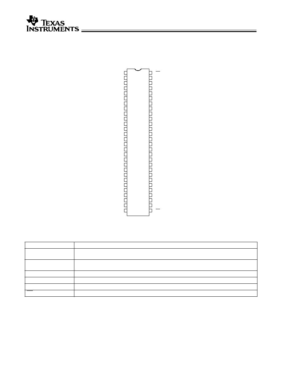
Pin Configuration
Pin Description
Pin Names
Description
A
Data Register A Inputs
Data Register B Outputs
B
Data Register B Inputs
Data Register A Outputs
CLKAB, CLKBA
Clock Pulse Inputs
SAB, SBA
Output Data Source Select Inputs
DIR
Direction
OE
Output Enable (Active LOW)
CY74FCT16646T
CY74FCT162646T
3
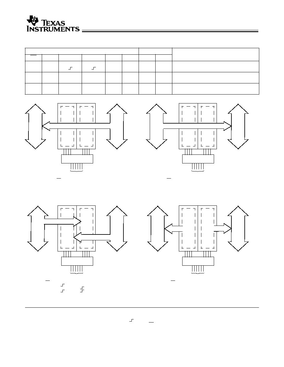
Function Table
[1]
Inputs
Data I/O
[2]
Function
OE
DIR
CLKAB
CLKBA
SAB
SBA
A
B
H
H
X
X
H or L
H or L
X
X
X
X
Input
Input
Isolation
Store A and B Data
L
L
L
L
X
X
X
H or L
X
X
L
H
Output
Input
Real Time B Data to A Bus
Stored B Data to A Bus
L
L
H
H
X
H or L
X
X
L
H
X
X
Input
Output
Real Time A Data to Bus
Stored A Data to B Bus
Notes:
1.
H = HIGH Voltage Level. L = LOW Voltage Level. X = Don't Care
.
= LOW-to-HIGH Transition
2.
The data output functions may be enabled or disabled by various signals at the OE or DIR inputs. Data input functions are always enabled, i.e., data at the
bus pins will be stored on every LOW-to-HIGH transition on the clock inputs.
3.
Cannot transfer data to A-bus and B-bus simultaneously.
BUS B
BUS A
DIR
L
OE
L
CLKAB
X
SAB
X
BUS B
BUS A
DIR
H
L
X
OE
L
L
H
CLKAB
X
SAB
X
X
X
SBA
X
X
X
BUS B
BUS A
DIR
H
OE
L
SAB
L
SBA
X
BUS A
BUS A
DIR
L
H
OE
L
L
SAB
X
H
SBA
H
X
Real-Time Transfer
Bus B to BusA
Real-Time Transfer
BusA to Bus B
Storage from
A and/or B
Transfer Stored Data
to A and/or B
CLKBA
X
CLKAB
X
CLKBA
X
SBA
L
CLKBA
X
CLKAB
X
H or L
CLKBA
H or L
X
[3]
CY74FCT16646T
CY74FCT162646T
4
Maximum Ratings
[4]
(Above which the useful life may be impaired. For user guide-
lines, not tested.)
Storage Temperature .....................Com'l
-
55
∞
C to +125
∞
C
Ambient Temperature with
Power Applied .................................Com'l
-
55
∞
C to +125
∞
C
DC Input Voltage
.................................................-
0.5V to +7.0V
DC Output Voltage
..............................................-
0.5V to +7.0V
DC Output Current
(Maximum Sink Current/Pin)
...........................-
60 to +120 mA
Power Dissipation .......................................................... 1.0W
Static Discharge Voltage............................................>2001V
(per MIL-STD-883, Method 3015)
Operating Range
Range
Ambient
Temperature
V
CC
Industrial
-
40
∞
C to +85
∞
C
5V
±
10%
Electrical Characteristics
Over the Operating Range
Parameter
Description
Test Conditions
Min.
Typ.
[5]
Max.
Unit
V
IH
Input HIGH Voltage
2.0
V
V
IL
Input LOW Voltage
0.8
V
V
H
Input Hysteresis
[6]
100
mV
V
IK
Input Clamp Diode Voltage
V
CC
=Min., I
IN
=
-
18 mA
-
0.7
-
1.2
V
I
IH
Input HIGH Current
V
CC
=Max., V
I
=V
CC
±
1
µ
A
I
IL
Input LOW Current
V
CC
=Max., V
I
=GND
±
1
µ
A
I
OZH
High Impedance Output Current
(Three-State Output pins)
V
CC
=Max., V
OUT
=2.7V
±
1
µ
A
I
OZL
High Impedance Output Current
(Three-State Output pins)
V
CC
=Max., V
OUT
=0.5V
±
1
µ
A
I
OS
Short Circuit Current
[7]
V
CC
=Max., V
OUT
=GND
-
80
-
140
-
200
mA
I
O
Output Drive Current
[7]
V
CC
=Max., V
OUT
=2.5V
-
50
-
180
mA
I
OFF
Power-Off Disable
V
CC
=0V, V
OUT
4.5V
[9]
±
1
µ
A
Output Drive Characteristics for CY74FCT16646T
Parameter
Description
Test Conditions
Min.
Typ.
[5]
Max.
Unit
V
OH
Output HIGH Voltage
V
CC
=Min., I
OH
=
-
3 mA
2.5
3.5
V
V
CC
=Min., I
OH
=
-
15 mA
2.4
3.5
V
V
CC
=Min., I
OH
=
-
32 mA
2.0
3.0
V
V
OL
Output LOW Voltage
V
CC
=Min., I
OL
=64 mA
0.2
0.55
V
Output Drive Characteristics for CY74FCT162646T
Parameter
Description
Test Conditions
Min.
Typ.
[5]
Max.
Unit
I
ODL
Output LOW Current
[7]
V
CC
=5V, V
IN
=V
IH
or V
IL
, V
OUT
=1.5V
60
115
150
mA
I
ODH
Output HIGH Current
[7]
V
CC
=5V, V
IN
=V
IH
or V
IL
, V
OUT
=1.5V
-
60
-
115
-
150
mA
V
OH
Output HIGH Voltage
V
CC
=Min., I
OH
=
-
24 mA
2.4
3.3
V
V
OL
Output LOW Voltage
V
CC
=Min., I
OL
=24 mA
0.3
0.55
V
Notes:
4.
Stresses greater than those listed under Maximum Ratings may cause permanent damage to the device. This is a stress rating only and functional operation
of the device at these or any other conditions above those indicated in the operational sections of this specification is not implied. Exposure to absolute
maximum rating conditions for extended periods may affect reliability.
5.
Typical values are at V
CC
= 5.0V, T
A
= +25∞C ambient.
6.
This parameter is specified but not tested.
7.
Not more than one output should be shorted at a time. Duration of short should not exceed one second. The use of high-speed test apparatus and/or sample
and hold techniques are preferable in order to minimize internal chip heating and more accurately reflect operational values. Otherwise prolonged shorting of
a high output may raise the chip temperature well above normal and thereby cause invalid readings in other parametrics tests. In any sequence of parameter
tests, I
OS
tests should be performed last.
8.
This parameter is measured at characterization but not tested.
9.
Tested at +25∞C.
CY74FCT16646T
CY74FCT162646T
5
Capacitance
(T
A
= +25∞C, f = 1.0 MHz)
Symbol
Description
[8]
Conditions
Typ.
Max.
Unit
C
IN
Input Capacitance
V
IN
= 0V
4.5
6.0
pF
C
OUT
Output Capacitance
V
OUT
=0V
5.5
8.0
pF
Power Supply Characteristics
Parameter
Description
Test Conditions
[10]
Min.
Typ.
[5]
Max.
Unit
I
CC
Quiescent Power Supply Current
V
CC
=Max.
V
IN
<0.2V
V
IN
>V
CC
-
0.2V
--
5
500
µ
A
I
CC
Quiescent Power Supply Current
TTL Inputs HIGH
V
CC
= Max.
V
IN
=3.4V
[11]
--
0.5
1.5
mA
I
CCD
Dynamic Power Supply
Current
[12]
V
CC
=Max.
Outputs Open
DIR=OE=GND
One-Bit Toggling
50% Duty Cycle
V
IN
=V
CC
or
V
IN
=GND
--
75
120
µ
A/MHz
I
C
Total Power Supply Current
[13]
V
CC
=Max.
Outputs Open
f
o
=10 MHz (CLKBA)
50% Duty Cycle
DIR=OE=GND
One-Bit Toggling
f
1
=5 MHz
50% Duty Cycle
V
IN
=V
CC
or
V
IN
=GND
--
0.8
1.7
mA
V
IN
=3.4V or
V
IN
=GND
--
1.3
3.2
V
CC
=Max.
Outputs Open
f
o
=10 MHz (CLKBA)
50% Duty Cycle
DIR=OE=GND
Sixteen-Bits Toggling
f
1
=2.5 MHz
50% Duty Cycle
V
IN
=V
CC
or
V
IN
=GND
--
3.8
6.5
[14]
V
IN
=3.4V or
V
IN
=GND
--
8.3
20.0
[14]
Notes:
10. For conditions shown as Max. or Min., use appropriate value specified under Electrical Characteristics for the applicable device type.
11. Per TTL driven input (V
IN
=3.4V); all other inputs at V
CC
or GND.
12. This parameter is not directly testable, but is derived for use in Total Power Supply calculations.
13. I
C
= I
QUIESCENT
+ I
INPUTS
+ I
DYNAMIC
I
C
= I
CC
+
I
CC
D
H
N
T
+I
CCD
(f
0
/2 + f
1
N
1
)
I
CC
= Quiescent Current with CMOS input levels
I
CC
= Power Supply Current for a TTL HIGH input (V
IN
=3.4V)
D
H
= Duty Cycle for TTL inputs HIGH
N
T
= Number of TTL inputs at D
H
I
CCD
= Dynamic Current caused by an input transition pair (HLH or LHL)
f
0
= Clock frequency for registered devices, otherwise zero
f
1
= Input signal frequency
N
1
= Number of inputs changing at f
1
All currents are in milliamps and all frequencies are in megahertz.
14. Values for these conditions are examples of the ICC formula. These limits are specified but not tested.
CY74FCT16646T
CY74FCT162646T
6
Switching Characteristics
Over the Operating Range
[15]
Parameter
Description
CY74FCT16646T
CY74FCT16646AT
CY74FCT162646AT
Unit
Min.
Max.
Min.
Max.
Fig. No.
[16]
t
PLH
t
PHL
Propagation Delay
Bus to Bus
1.5
9.0
1.5
6.3
ns
1, 2
t
PZH
t
PZL
Output Enable Time
DIR or OE to Bus
1.5
14.0
1.5
9.8
ns
1, 7, 8
t
PHZ
t
PLZ
Output Disable Time
DIR or OE to Bus
1.5
9.0
1.5
6.3
ns
1, 7, 8
t
PLH
t
PHL
Propagation Delay
Clock to Bus
1.5
9.0
1.5
6.3
ns
1, 5
t
PLH
t
PHL
Propagation Delay
SBA or SAB to Bus
1.5
11.0
1.5
7.7
ns
1,5
t
SU
Set-Up Time HIGH or
LOW Bus to Clock
2.0
--
2.0
--
ns
4
t
H
Hold Time HIGH or
LOW Bus to Clock
1.5
--
1.5
--
ns
4
t
W
Clock Pulse Width
HIGH or LOW
5.0
--
5.0
--
ns
6
t
SK(O)
Output Skew
[17]
--
0.5
--
0.5
ns
--
Parameter
Description
CY74FCT16646CT
CY74FCT162646CT
CY74FCT16646ET
CY74FCT162646ET
Unit
Min.
Max.
Min.
Max.
Fig. No.
[16]
t
PLH
t
PHL
Propagation Delay
Bus to Bus
1.5
5.4
1.5
3.8
ns
1, 2
t
PZH
t
PZL
Output Enable Time
DIR or OE to Bus
1.5
7.8
1.5
4.8
ns
1, 7, 8
t
PHZ
t
PLZ
Output Disable Time
DIR or OE to Bus
1.5
6.3
1.5
4.0
ns
1, 7, 8
t
PLH
t
PHL
Propagation Delay
Clock to Bus
1.5
5.7
1.5
3.8
ns
1, 5
t
PLH
t
PHL
Propagation Delay
SBA or SAB to Bus
1.5
6.2
1.5
4.2
ns
1,5
t
SU
Set-Up Time HIGH or
LOW Bus to Clock
2.0
--
2.0
--
ns
4
t
H
Hold Time HIGH or
LOW Bus to Clock
1.5
--
0.0
--
ns
4
t
W
Clock Pulse Width
HIGH or LOW
5.0
--
3.0
--
ns
6
t
SK(O)
Output Skew
[17]
--
0.5
--
0.5
ns
--
Notes:
15. Minimum limits are specified but not tested on Propagation Delays.
16. See "Parameter Measurement Information" in the General Information section.
17. Skew any two outputs of the same package switching in the same direction. This parameter is ensured by design.
CY74FCT16646T
CY74FCT162646T
7
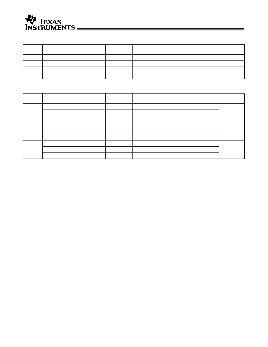
Ordering Information CY74FCT16646
Speed
(ns)
Ordering Code
Package
Name
Package Type
Operating
Range
3.8
CY74FCT16646ETPVC/PVCT
O56
56-Lead (300-Mil) SSOP
Industrial
5.4
CY74FCT16646CTPVC/PVCT
O56
56-Lead (300-Mil) SSOP
Industrial
6.3
CY74FCT16646ATPVC/PVCT
O56
56-Lead (300-Mil) SSOP
Industrial
9.0
CY74FCT16646TPVC/PVCT
O56
56-Lead (300-Mil) SSOP
Industrial
Ordering Information CY74FCT162646
Speed
(ns)
Ordering Code
Package
Name
Package Type
Operating
Range
3.8
74FCT162646ETPACT
Z56
56-Lead (240-Mil) TSSOP
Industrial
CY74FCT162646ETPVC
O56
56-Lead (300-Mil) SSOP
74FCT162646ETPVCT
O56
56-Lead (300-Mil) SSOP
5.4
74FCT162646CTPACT
Z56
56-Lead (240-Mil) TSSOP
Industrial
CY74FCT162646CTPVC
O56
56-Lead (300-Mil) SSOP
74FCT162646CTPVCT
O56
56-Lead (300-Mil) SSOP
6.3
74FCT162646ATPACT
Z56
56-Lead (240-Mil) TSSOP
Industrial
CY74FCT162646ATPVC
O56
56-Lead (300-Mil) SSOP
74FCT162646ATPVCT
O56
56-Lead (300-Mil) SSOP
CY74FCT16646T
CY74FCT162646T
8
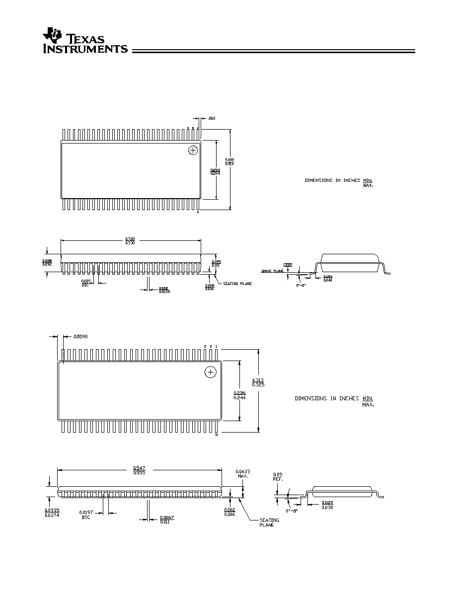
Package Diagrams
56-Lead Shrunk Small Outline Package O56
56-Lead Thin Shrunk Small Outline Package Z56

IMPORTANT NOTICE
Texas Instruments and its subsidiaries (TI) reserve the right to make changes to their products or to discontinue
any product or service without notice, and advise customers to obtain the latest version of relevant information
to verify, before placing orders, that information being relied on is current and complete. All products are sold
subject to the terms and conditions of sale supplied at the time of order acknowledgement, including those
pertaining to warranty, patent infringement, and limitation of liability.
TI warrants performance of its semiconductor products to the specifications applicable at the time of sale in
accordance with TI's standard warranty. Testing and other quality control techniques are utilized to the extent
TI deems necessary to support this warranty. Specific testing of all parameters of each device is not necessarily
performed, except those mandated by government requirements.
CERTAIN APPLICATIONS USING SEMICONDUCTOR PRODUCTS MAY INVOLVE POTENTIAL RISKS OF
DEATH, PERSONAL INJURY, OR SEVERE PROPERTY OR ENVIRONMENTAL DAMAGE ("CRITICAL
APPLICATIONS"). TI SEMICONDUCTOR PRODUCTS ARE NOT DESIGNED, AUTHORIZED, OR
WARRANTED TO BE SUITABLE FOR USE IN LIFE-SUPPORT DEVICES OR SYSTEMS OR OTHER
CRITICAL APPLICATIONS. INCLUSION OF TI PRODUCTS IN SUCH APPLICATIONS IS UNDERSTOOD TO
BE FULLY AT THE CUSTOMER'S RISK.
In order to minimize risks associated with the customer's applications, adequate design and operating
safeguards must be provided by the customer to minimize inherent or procedural hazards.
TI assumes no liability for applications assistance or customer product design. TI does not warrant or represent
that any license, either express or implied, is granted under any patent right, copyright, mask work right, or other
intellectual property right of TI covering or relating to any combination, machine, or process in which such
semiconductor products or services might be or are used. TI's publication of information regarding any third
party's products or services does not constitute TI's approval, warranty or endorsement thereof.
Copyright
©
2000, Texas Instruments Incorporated