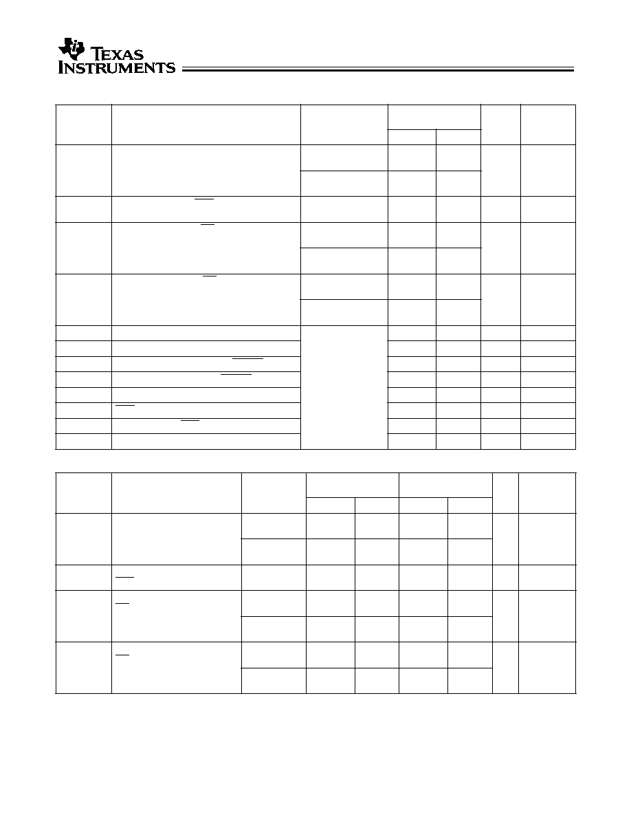
18-Bit Registers
CY74FCT16823T
CY74FCT162823T
SCCS062 - August 1994 - Revised March 2000
Data sheet acquired from Cypress Semiconductor Corporation.
Data sheet modified to remove devices not offered.
Copyright
©
2000, Texas Instruments Incorporated
Features
∑ FCT-E speed at 4.4 ns
∑ Power-off disable outputs permits live insertion
∑ Edge-rate control circuitry for significantly improved
noise characteristics
∑ Typical output skew < 250 ps
∑ ESD > 2000V
∑ TSSOP (19.6-mil pitch) and SSOP (25-mil pitch)
packages
∑ Industrial temperature range of
-
40∞C to +85∞C
∑ V
CC
= 5V
±
10%
CY74FCT16823T Features:
∑ 64 mA sink current, 32 mA source current
∑ Typical V
OLP
(ground bounce) <1.0V at V
CC
= 5V,
T
A
= 25∞C
CY74FCT162823T Features:
∑ Balanced 24 mA output drivers
∑ Reduced system switching noise
∑ Typical V
OLP
(ground bounce) <0.6V at V
CC
= 5V,
T
A
= 25∞C
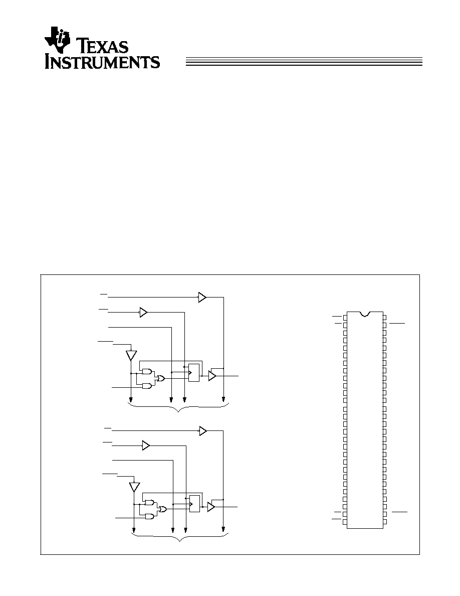
Functional Description
The CY74FCT16823T and the CY74FCT162823T 18-bit bus
interface registers are designed for use in high-speed,
low-power systems needing wide registers and parity. 18-bit
operation is achieved by connecting the control lines of the two
9-bit
registers.
Flow-through
pinout
and
small
shrink
packaging aids in simplifying board layout. The outputs are
designed with a power-off disable feature to allow live insertion
of boards.
The
CY74FCT16823T
is
ideally
suited
for
driving
high-capacitance loads and low-impedance backplanes.
The CY74FCT162823T has 24-mA balanced output drivers
with current limiting resistors in the outputs. This reduces the
need for external terminating resistors and provides for
minimal undershoot and reduced ground bounce. The
CY74FCT162823T is ideal for driving transmission lines.
Logic Block Diagrams
C
Pin Configuration
D
R
1
2
3
4
5
6
7
8
9
10
11
12
33
32
31
30
29
36
35
1
CLR
34
SSOP/TSSOP
Top View
13
15
16
17
18
19
20
21
22
23
24
45
44
43
42
41
37
38
39
40
48
47
46
1
CLR
1
D
1
1
OE
1
OE
1
Q
1
1
Q
2
GND
V
CC
GND
FCT16823-1
1
CLK
1
CLKEN
1
Q
1
TO 8 OTHER CHANNELS
GND
1
D
1
1
D
2
1
D
3
1
D
4
1
CLK
GND
1
D
5
1
D
6
1
D
7
1
D
9
V
CC
GND
2
D
1
2
D
2
2
D
4
GND
2
D
5
2
D
6
2
D
7
2
D
8
V
CC
2
CLK
1
CLKEN
25
26
27
28
49
50
51
52
53
54
55
56
1
D
8
2
D
3
2
D
9
2
CLKEN
C
D
R
2
CLR
2
D
2
2
OE
2
CLK
2
CLKEN
2
Q
1
TO 8 OTHER CHANNELS
1
Q
3
1
Q
4
1
Q
5
1
Q
7
1
Q
8
1
Q
9
1
Q
6
14
2
Q
1
2
Q
2
2
Q
3
2
Q
4
2
Q
6
2
Q
7
2
Q
8
2
Q
5
2
Q
9
GND
V
CC
GND
2
OE
2
CLR
FCT16823-2
FCT16823-3
CY74FCT16823T
CY74FCT162823T
2
Maximum Ratings
[3, 4]
(Above which the useful life may be impaired. For user
guidelines, not tested.)
Storage Temperature
.....................................-
55
∞
C to +125
∞
C
Ambient Temperature with
Power Applied
..................................................-
55
∞
C to +125
∞
C
DC Input Voltage
.................................................-
0.5V to +7.0V
DC Output Voltage
..............................................-
0.5V to +7.0V
DC Output Current
(Maximum Sink Current/Pin)
...........................-
60 to +120 mA
Power Dissipation .......................................................... 1.0W
Static Discharge Voltage............................................>2001V
(per MIL-STD-883, Method 3015)
Notes:
1.
H = HIGH Voltage Level.
L = LOW Voltage Level.
X = Don't Care.
Z = HIGH Impedance.
=LOW-to-HIGH transition.
2.
Output level before indicated steady-state input conditions were established.
3.
Operation beyond the limits set forth may impair the useful life of the device. Unless otherwise noted, these limits are over the operating free-air temperature range.
4.
Unused inputs must always be connected to an appropriate logic voltage level, preferably either V
CC
or ground.
Pin Description
Name
Description
D
Data Inputs
CLK
Clock Inputs
CLKEN
Clock Enable Inputs (Active LOW)
CLR
Asynchronous Clear Inputs (Active LOW)
OE
Output Enable Inputs (Active LOW)
Q
Three-State Outputs
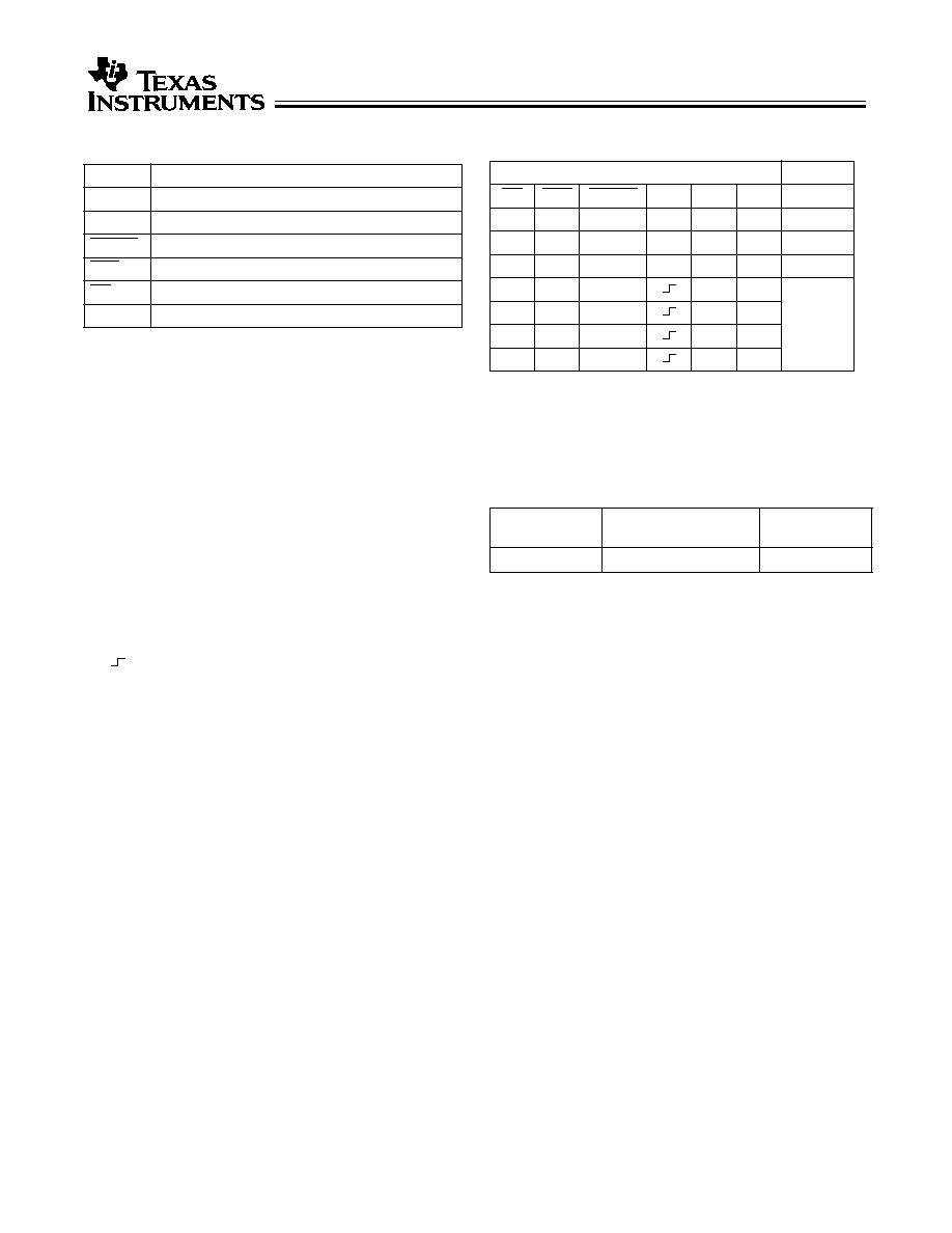
Function Table
[1]
Inputs
Outputs
OE
CLR
CLKEN
CLK
D
Q
Function
H
X
X
X
X
Z
High Z
L
L
X
X
X
L
Clear
L
H
H
X
X
Q
[2]
Hold
H
H
L
L
Z
Load
H
H
L
H
Z
L
H
L
L
L
L
H
L
H
H
Operating Range
Range
Ambient
Temperature
V
CC
Industrial
-
40
∞
C to +85
∞
C
5V
±
10%
CY74FCT16823T
CY74FCT162823T
3
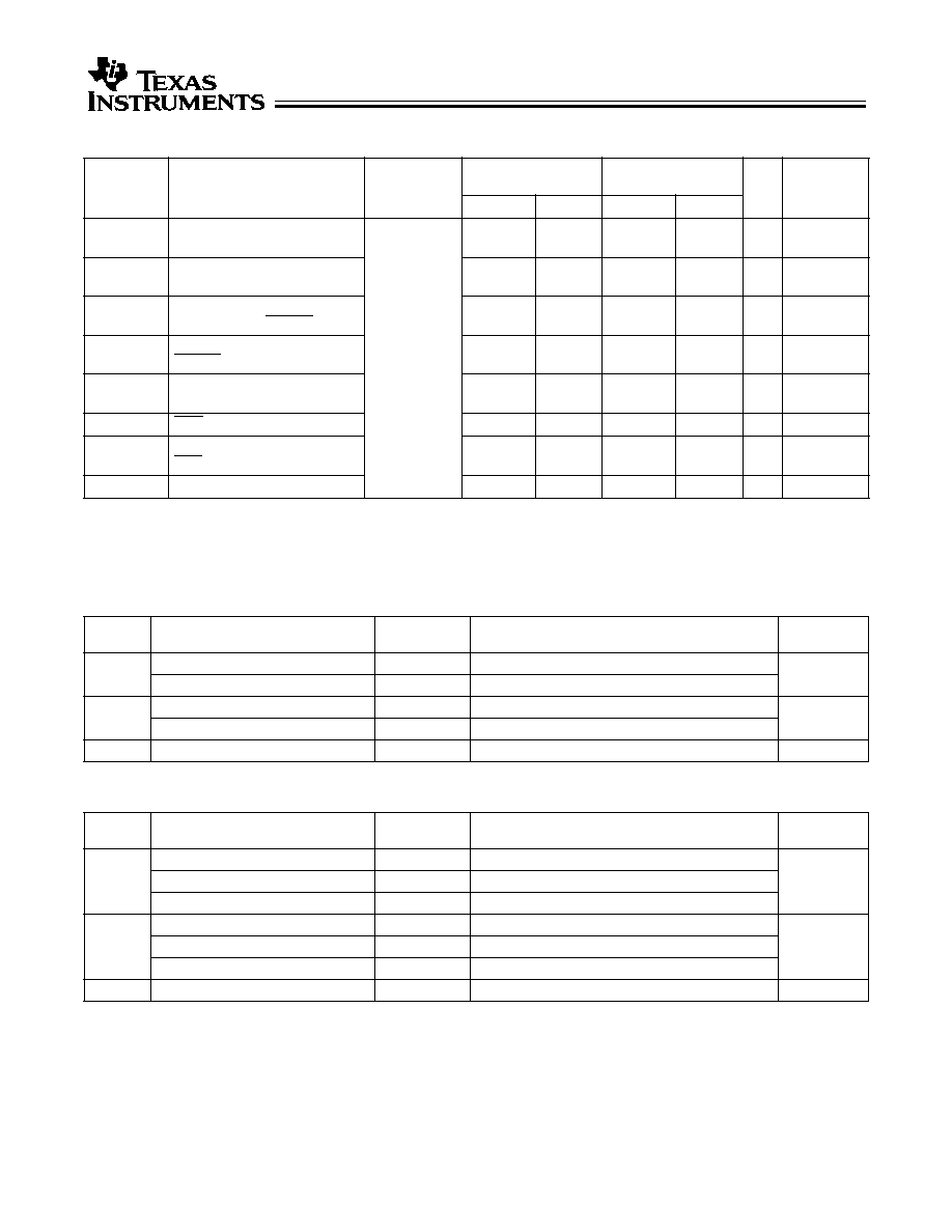
Electrical Characteristics
Over the Operating Range
Parameter
Description
Test Conditions
Min.
Typ.
[5]
Max.
Unit
V
IH
Input HIGH Voltage
2.0
V
V
IL
Input LOW Voltage
0.8
V
V
H
Input Hysteresis
[6]
100
mV
V
IK
Input Clamp Diode Voltage
V
CC
=Min., I
IN
=
-
18 mA
-
0.7
-
1.2
V
I
IH
Input HIGH Current
V
CC
=Max., V
I
=V
CC
±
1
µ
A
I
IL
Input LOW Current
V
CC
=Max., V
I
=GND
±
1
µ
A
I
OZH
High Impedance Output Current
(Three-State Output pins)
V
CC
=Max., V
OUT
=2.7V
±
1
µ
A
I
OZL
High Impedance Output Current
(Three-State Output pins)
V
CC
=Max., V
OUT
=0.5V
±
1
µ
A
I
OS
Short Circuit Current
[7]
V
CC
=Max., V
OUT
=GND
-
80
-
140
-
200
mA
I
O
Output Drive Current
[7]
V
CC
=Max., V
OUT
=2.5V
-
50
-
180
mA
I
OFF
Power-Off Disable
V
CC
=0V, V
OUT
4.5V
[8]
1
µ
A
Output Drive Characteristics for CY74FCT16823T
Parameter
Description
Test Conditions
Min.
Typ.
[5]
Max.
Unit
V
OH
Output HIGH Voltage
V
CC
=Min., I
OH
=
-
3 mA
2.5
3.5
V
V
CC
=Min., I
OH
=
-
15 mA
2.4
3.5
V
CC
=Min., I
OH
=
-
32 mA
2.0
3.0
V
OL
Output LOW Voltage
V
CC
=Min., I
OL
=64 mA
0.2
0.55
V
Output Drive Characteristics for CY74FCT162823T
Parameter
Description
Test Conditions
Min.
Typ.
[5]
Max.
Unit
I
ODL
Output LOW Voltage
[7]
V
CC
=5V, V
IN
=V
IH
or V
IL
, V
OUT
=1.5V
60
115
150
mA
I
ODH
Output HIGH Voltage
[7]
V
CC
=5V, V
IN
=V
IH
or V
IL
, V
OUT
=1.5V
-
60
-
115
-
150
mA
V
OH
Output HIGH Voltage
V
CC
=Min., I
OH
=
-
24 mA
2.4
3.3
V
V
OL
Output LOW Voltage
V
CC
=Min., I
OL
=24 mA
0.3
0.55
V
Capacitance
[9]
(T
A
= +25∞C, f = 1.0 MHz)
Parameter
Description
Test Conditions
Typ.
[5]
Max.
Unit
C
IN
Input Capacitance
V
IN
= 0V
4.5
6.0
pF
C
OUT
Output Capacitance
V
OUT
= 0V
5.5
8.0
pF
Notes:
5.
Typical values are at V
CC
= 5.0V, T
A
= +25∞C ambient.
6.
This input is specified but not tested.
7.
Not more than one output should be shorted at a time. Duration of short should not exceed one second. The use of high-speed test apparatus and/or sample
and hold techniques are preferable in order to minimize internal chip heating and more accurately reflect operational values. Otherwise prolonged shorting
of a high output may raise the chip temperature well above normal and thereby cause invalid readings in other parametric tests. In any sequence of parameter
tests, I
OS
tests should be performed last.
8.
Tested at +25∞C.
9.
This parameter is specified but not tested.
CY74FCT16823T
CY74FCT162823T
4
Power Supply Characteristics
Parameter
Description
Test Conditions
[10]
Min.
Typ.
[5]
Max.
Unit
I
CC
Quiescent Power Supply
Current
V
CC
=Max.
V
IN
<0.2V
V
IN
>V
CC
-
0.2V
--
5
500
µ
A
I
CC
Quiescent Power Supply
Current (TTL inputs HIGH)
V
CC
=Max.
V
IN
=3.4V
[11]
--
0.5
1.5
mA
I
CCD
Dynamic Power Supply
Current
[12]
V
CC
=Max.,
One Input Toggling,
50% Duty Cycle,
Outputs Open,
OE=CLKEN=GND
V
IN
=V
CC
or
V
IN
=GND
--
75
120
µ
A/
MHz
I
C
Total Power Supply Current
[13]
V
CC
=Max.,
f
0
=10 MHz,
50% Duty Cycle,
Outputs Open,
One Bit Toggling,
OE=CLKEN=GND
at f
1
=5 MHz
V
IN
=V
CC
or
V
IN
=GND
--
0.8
1.7
mA
V
IN
=3.4V or
V
IN
=GND
--
1.3
3.2
V
CC
=Max.,
at f
1
=2.5 MHz,
50% Duty Cycle,
Outputs Open,
Eighteen Bits Toggling,
OE=CLKEN=GND
f
0
=10 MHz
V
IN
=V
CC
or
V
IN
=GND
--
4.2
7.1
[14]
V
IN
=3.4V or
V
IN
=GND
--
9.2
22.1
[14]
Notes:
10. For conditions shown as Max. or Min., use appropriate value specified under Electrical Characteristics for the applicable device type.
11. Per TTL driven input (V
IN
=3.4V); all other inputs at V
CC
or GND.
12. This parameter is not directly testable, but is derived for use in Total Power Supply calculations.
13. I
C
=
I
QUIESCENT
+ I
INPUTS
+ I
DYNAMIC
I
C
=
I
CC
+
I
CC
D
H
N
T
+I
CCD
(f
0
/2 + f
1
N
1
)
I
CC
=
Quiescent Current with CMOS input levels
I
CC
=
Power Supply Current for a TTL HIGH input (V
IN
=3.4V)
D
H
=
Duty Cycle for TTL inputs HIGH
N
T
=
Number of TTL inputs at D
H
I
CCD
=
Dynamic Current caused by an input transition pair (HLH or LHL)
f
0
=
Clock frequency for registered devices, otherwise zero
f
1
=
Input signal frequency
N
1
=
Number of inputs changing at f
1
All currents are in milliamps and all frequencies are in megahertz.
14. Values for these conditions are examples of the I
CC
formula. These limits are specified but not tested.
CY74FCT16823T
CY74FCT162823T
5
Switching Characteristics
Over the Operating Range
[15]
CY74FCT16823AT
CY74FCT162823AT
Parameter
Description
Condition
[16]
Min.
Max.
Unit
Fig.No.
[16]
t
PLH
t
PHL
Propagation Delay CLK to Q
C
L
=50 pF
R
L
=500
1.5
10.0
ns
1, 5
C
L
=300 pF
[17]
R
L
=500
1.5
20.0
t
PHL
Propagation Delay CLR to Q
C
L
=50 pF
R
L
=500
1.5
14.0
ns
1, 5
t
PZH
t
PZL
Output Enable Time OE to Q
C
L
=50 pF
R
L
=500
1.5
12.0
ns
1, 7, 8
C
L
=300 pF
[17]
R
L
=500
1.5
23.0
t
PHZ
t
PLZ
Output Disable Time OE to Q
C
L
=5 pF
[17]
R
L
=500
1.5
7.0
ns
1, 7, 8
C
L
=50 pF
R
L
=500
1.5
8.0
t
SU
Set-Up Time HIGH or LOW, D to CLK
C
L
=50 pF
R
L
=500
3.0
--
ns
4
t
H
Hold Time HIGH or LOW, D to CLK
1.5
--
ns
4
t
SU
Set-Up Time HIGH or LOW, CLKEN to CLK
3.0
--
ns
9
t
H
Hold Time HIGH or LOW CLKEN to CLK
0.0
--
ns
9
t
W
CLK Pulse Width HIGH or LOW
6.0
--
ns
5
t
W
CLR Pulse Width LOW
6.0
--
ns
5
t
REM
Recovery Time CLR to CLK
6.0
--
ns
6
t
SK(O)
Output Skew
[18]
--
0.5
ns
--
Switching Characteristics
Over the Operating Range
[15]
CY74FCT16823CT
CY74FCT162823CT
CY74FCT16823ET
CY74FCT162823ET
Parameter
Description
Condition
[16]
Min.
Max.
Min.
Max.
Unit
Fig.No.
[16]
t
PLH
t
PHL
Propagation Delay
CLK to Q
C
L
=50 pF
R
L
=500
1.5
6.0
1.5
4.4
ns
1, 5
C
L
=300 pF
[17]
R
L
=500
1.5
12.5
1.5
8.0
t
PHL
Propagation Delay
CLR to Q
C
L
=50 pF
R
L
=500
1.5
6.1
1.5
4.4
ns
1, 5
t
PZH
t
PZL
Output Enable Time
OE to Q
C
L
=50 pF
R
L
=500
1.5
5.5
1.5
4.4
ns
1, 7, 8
C
L
=300 pF
[17]
R
L
=500
1.5
12.5
1.5
9.0
t
PHZ
t
PLZ
Output Disable Time
OE to Q
C
L
=5 pF
[17]
R
L
=500
1.5
5.2
1.5
3.6
ns
1, 7, 8
C
L
=50 pF
R
L
=500
1.5
6.5
1.5
3.6
CY74FCT16823T
CY74FCT162823T
6
t
SU
Set-Up Time
HIGH or LOW, D to CLK
C
L
=50 pF
R
L
=500
2.0
--
1.5
--
ns
4
t
H
Hold Time
HIGH or LOW, D to CLK
1.5
--
0.0
--
ns
4
t
SU
Set-Up Time
HIGH or LOW, CLKEN to CLK
3.0
--
2.5
--
ns
9
t
H
Hold Time HIGH or LOW
CLKEN to CLK
0.0
--
0.0
--
ns
9
t
W
CLK Pulse Width
HIGH or LOW
3.3
--
3.3
--
ns
5
t
W
CLR Pulse Width LOW
3.3
--
3.0
--
ns
5
t
REM
Recovery Time
CLR to CLK
6.0
--
3.0
--
ns
6
t
SK(O)
Output Skew
[18]
--
0.5
--
0.5
ns
--
Notes:
15. Minimum limits are specified but not tested on Propagation Delays.
16. See "Parameter Measurement Information" in the General Information section.
17. These limits are specified but not tested.
18. Skew between any two outputs of the same package switching in the same direction. This parameter is ensured by design.
Switching Characteristics
Over the Operating Range
[15]
(continued)
CY74FCT16823CT
CY74FCT162823CT
CY74FCT16823ET
CY74FCT162823ET
Parameter
Description
Condition
[16]
Min.
Max.
Min.
Max.
Unit
Fig.No.
[16]
Ordering Information CY74FCT16823
Speed
(ns)
Ordering Code
Package
Name
Package Type
Operating
Range
4.4
CY74FCT16823ETPACT
Z56
56-Lead (240-Mil) TSSOP
Industrial
CY74FCT16823ETPVC/PVCT
O56
56-Lead (300-Mil) SSOP
6.0
CY74FCT16823CTPACT
Z56
56-Lead (240-Mil) TSSOP
Industrial
CY74FCT16823CTPVC/PVCT
O56
56-Lead (300-Mil) SSOP
10.0
CY74FCT16823ATPACT
Z56
56-Lead (240-Mil) TSSOP
Industrial
Ordering Information CY74FCT162823
Speed
(ns)
Ordering Code
Package
Name
Package Type
Operating
Range
4.4
74FCT162823ETPACT
Z56
56-Lead (240-Mil) TSSOP
Industrial
CY74FCT162823ETPVC
O56
56-Lead (300-Mil) SSOP
74FCT162823ETPVCT
O56
56-Lead (300-Mil) SSOP
6.0
74FCT162823CTPACT
Z56
56-Lead (240-Mil) TSSOP
Industrial
CY74FCT162823CTPVC
O56
56-Lead (300-Mil) SSOP
74FCT162823CTPVCT
O56
56-Lead (300-Mil) SSOP
10.0
74FCT162823ATPACT
Z56
56-Lead (240-Mil) TSSOP
Industrial
CY74FCT16823T
CY74FCT162823T
7
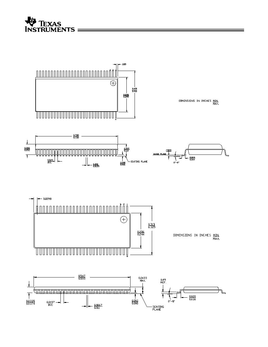
Package Diagrams
56-Lead Shrunk Small Outline Package O56
56-Lead Thin Shrunk Small Outline Package Z56

IMPORTANT NOTICE
Texas Instruments and its subsidiaries (TI) reserve the right to make changes to their products or to discontinue
any product or service without notice, and advise customers to obtain the latest version of relevant information
to verify, before placing orders, that information being relied on is current and complete. All products are sold
subject to the terms and conditions of sale supplied at the time of order acknowledgement, including those
pertaining to warranty, patent infringement, and limitation of liability.
TI warrants performance of its semiconductor products to the specifications applicable at the time of sale in
accordance with TI's standard warranty. Testing and other quality control techniques are utilized to the extent
TI deems necessary to support this warranty. Specific testing of all parameters of each device is not necessarily
performed, except those mandated by government requirements.
CERTAIN APPLICATIONS USING SEMICONDUCTOR PRODUCTS MAY INVOLVE POTENTIAL RISKS OF
DEATH, PERSONAL INJURY, OR SEVERE PROPERTY OR ENVIRONMENTAL DAMAGE ("CRITICAL
APPLICATIONS"). TI SEMICONDUCTOR PRODUCTS ARE NOT DESIGNED, AUTHORIZED, OR
WARRANTED TO BE SUITABLE FOR USE IN LIFE-SUPPORT DEVICES OR SYSTEMS OR OTHER
CRITICAL APPLICATIONS. INCLUSION OF TI PRODUCTS IN SUCH APPLICATIONS IS UNDERSTOOD TO
BE FULLY AT THE CUSTOMER'S RISK.
In order to minimize risks associated with the customer's applications, adequate design and operating
safeguards must be provided by the customer to minimize inherent or procedural hazards.
TI assumes no liability for applications assistance or customer product design. TI does not warrant or represent
that any license, either express or implied, is granted under any patent right, copyright, mask work right, or other
intellectual property right of TI covering or relating to any combination, machine, or process in which such
semiconductor products or services might be or are used. TI's publication of information regarding any third
party's products or services does not constitute TI's approval, warranty or endorsement thereof.
Copyright
©
2000, Texas Instruments Incorporated