16-Bit Registered Transceivers
CY74FCT16952T
CY74FCT162952T
CY74FCT162H952T
Data sheet acquired from Cypress Semiconductor Corporation.
Data sheet modified to remove devices not offered.
SCCS065C - August 1994 - Revised September 2001
Copyright
©
2001, Texas Instruments Incorporated
1CY74FCT162H952
T
Features
∑ I
off
supports partial-power-down mode operation
∑ Edge-rate control circuitry for significantly improved
noise characteristics
∑ Typical output skew < 250 ps
∑ ESD > 2000V
∑ TSSOP (19.6-mil pitch) and SSOP (25-mil pitch)
packages
∑ Industrial temperature range of ≠40∞C to +85∞C
∑ V
CC
= 5V
±
10%
CY74FCT16952T Features:
∑ 64 mA sink current, 32 mA source current
∑ Typical V
OLP
(ground bounce) <1.0V at
V
CC
= 5V, T
A
= 25∞C
CY74FCT162952T Features:
∑ Balanced 24 mA output drivers
∑ Reduced system switching noise
∑ Typical V
OLP
(ground bounce) <0.6V at
V
CC
= 5V, T
A
= 25∞C
CY74FCT162H952T Features:
∑ Bus hold retains last active state
∑ Eliminates the need for external pull-up or pull-down
resistors
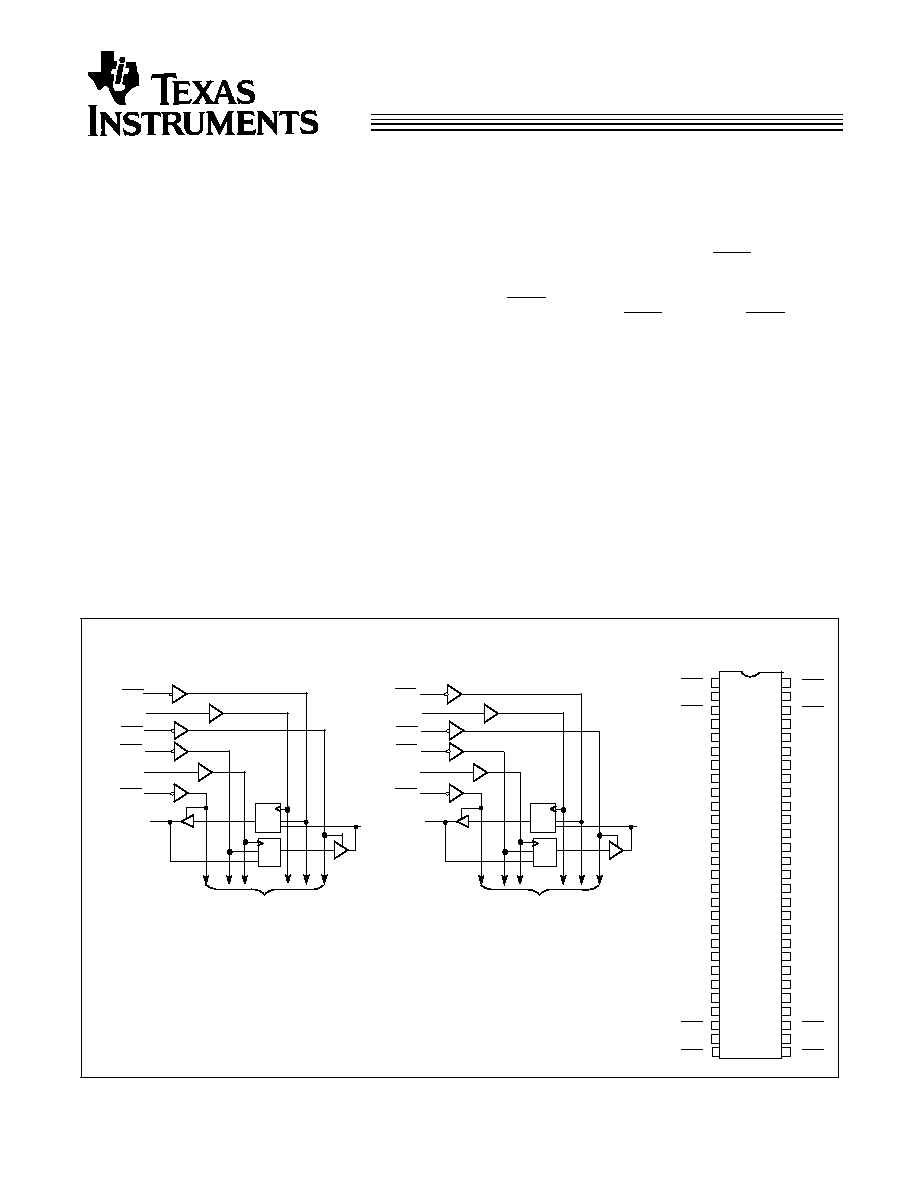
Functional Description
These
16-bit
registered
transceivers
are
high-speed,
low-power devices. 16-bit operation is achieved by connecting
the control lines of the two 8-bit registered transceivers
together. For data flow from bus A-to-B, CEAB must be LOW
to allow data to be stored when CLKAB transitions from
LOW-to-HIGH. The stored data will be present on the output
when OEAB is LOW. Control of data from B-to-A is similar and
is controlled by using the CEBA, CLKBA, and OEBA inputs.
This
device
is
fully
specified
for
partial-power-down
applications using I
off
. The I
off
circuitry disables the outputs,
preventing damaging current backflow through the device
when it is powered down.
The
CY74FCT16952T
is
ideally
suited
for
driving
high-capacitance loads and low-impedance backplanes.
The CY74FCT162952T has 24-mA balanced output drivers
with current-limiting resistors in the outputs. This reduces the
need for external terminating resistors and provides for
minimal undershoot and reduced ground bounce. The
CY74FCT162952T is ideal for driving transmission lines.
The CY74FCT162H952T is a 24-mA balanced output part that
has "bus hold" on the data inputs. The device retains the
input's last state whenever the input goes to high impedance.
This eliminates the need for pull-up/down resistors and
prevents floating inputs.
Logic Block Diagrams
Pin Configuration
1
OEAB
SSOP/TSSOP
Top View
1
CLKBA
1
B
1
1
B
2
GND
V
CC
GND
GND
FCT16952≠1
1
B
1
TO 7 OTHER CHANNELS
1
2
3
4
5
6
7
8
9
10
11
12
13
14
15
16
17
18
19
20
21
22
23
24
25
26
27
28
56
55
54
53
52
51
50
49
48
47
46
45
44
43
42
41
40
39
38
37
36
35
34
33
32
31
30
29
1
CEBA
1
OEAB
1
CEAB
1
CLKAB
1
OEBA
1
A
1
D
C
CE
D
C
CE
1
CEAB
1
CLKAB
GND
1
A
1
1
A
2
1
A
3
1
A
4
GND
2
A
1
2
A
2
2
A
3
2
A
4
V
CC
1
A
5
1
A
6
1
A
7
1
A
8
GND
2
A
5
2
A
6
2
A
7
2
A
8
2
CLKAB
GND
2
OEAB
2
CEAB
V
CC
1
OEBA
1
CEBA
1
CLKBA
GND
2
CLKBA
2
OEBA
2
CEBA
1
B
3
1
B
6
1
B
7
1
B
8
1
B
4
1
B
5
2
B
1
2
B
3
2
B
4
2
B
2
2
B
5
2
B
6
2
B
7
2
B
8
V
CC
2
CLKBA
2
B
1
2
OEAB
2
CEAB
2
CLKAB
2
OEBA
2
A
1
D
C
CE
D
C
CE
2
CEBA
FCT16952≠2
FCT16952≠3
TO 7 OTHER CHANNELS
CY74FCT16952T
CY74FCT162952T
CY74FCT162H952T
2
Maximum Ratings
[5, 6]
(Above which the useful life may be impaired. For user
guidelines, not tested.)
Storage Temperature ................................. ≠55
∞
C to +125
∞
C
Ambient Temperature with
Power Applied............................................. ≠55
∞
C to +125
∞
C
DC Input Voltage ........................................... ≠0.5V to +7.0V
DC Output Voltage......................................... ≠0.5V to +7.0V
DC Output Current
(Maximum Sink Current/Pin) ........................≠60 to +120 mA
Power Dissipation .......................................................... 1.0W
Static Discharge Voltage............................................>2001V
(per MIL-STD-883, Method 3015)
Notes:
1.
On the CY74FCT162H952T these pins have bus hold.
2.
A-to-B data flow is shown: B-to-A data flow is similar but uses, CEBA, CLKBA, and OEBA.
3.
H = HIGH Voltage Level.
L = LOW Voltage Level.
X = Don't Care.
= LOW-to-HIGH Transition.
Z = HIGH Impedance.
4.
Level of B before the indicated steady-state input conditions were established.
5.
Operation beyond the limits set forth may impair the useful life of the device. Unless otherwise noted, these limits are over the operating free-air temperature range.
6.
Unused inputs must always be connected to an appropriate logic voltage level, preferably either V
CC
or ground.
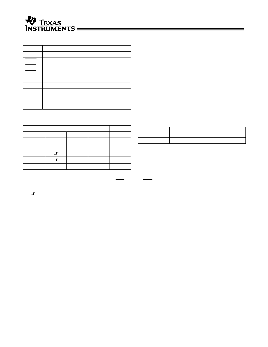
Pin Description
Name
Description
OEAB
A-to-B Output Enable Input (Active LOW)
OEBA
B-to-A Output Enable Input (Active LOW)
CEAB
A-to-B Clock Enable Input (Active LOW)
CEBA
B-to-A Clock Enable Input (Active LOW)
CLKAB
A-to-B Clock Input
CLKBA
B-to-A Clock Input
A
A-to-B Data Inputs or B-to-A Three-State
Outputs
[1]
B
B-to-A Data Inputs or A-to-B Three-State
Outputs
[1]
Function Table
[2, 3]
For A-to-B (Symmetric with B-to-A)
Inputs
Outputs
CEAB
CLKAB
OEAB
A
B
H
X
L
X
B
[4]
X
L
L
X
B
[4]
L
L
L
L
L
L
H
H
X
X
H
X
Z
Operating Range
Range
Ambient
Temperature
V
CC
Industrial
≠40
∞
C to +85
∞
C
5V
±
10%

CY74FCT16952T
CY74FCT162952T
CY74FCT162H952T
3
Note:
7.
Typical values are at V
CC
= 5.0V, T
A
= +25∞C ambient.
8.
This parameter is specified but not tested.
9.
Pins with bus hold are described in the Pin Description.
10. Not more than one output should be shorted at a time. Duration of short should not exceed one second. The use of high-speed test apparatus and/or sample
and hold techniques are preferable in order to minimize internal chip heating and more accurately reflect operational values. Otherwise prolonged shorting of a
high output may raise the chip temperature well above normal and thereby cause invalid readings in other parametric tests. In any sequence of parameter tests,
I
OS
tests should be performed last.
11. Tested at +25∞C.
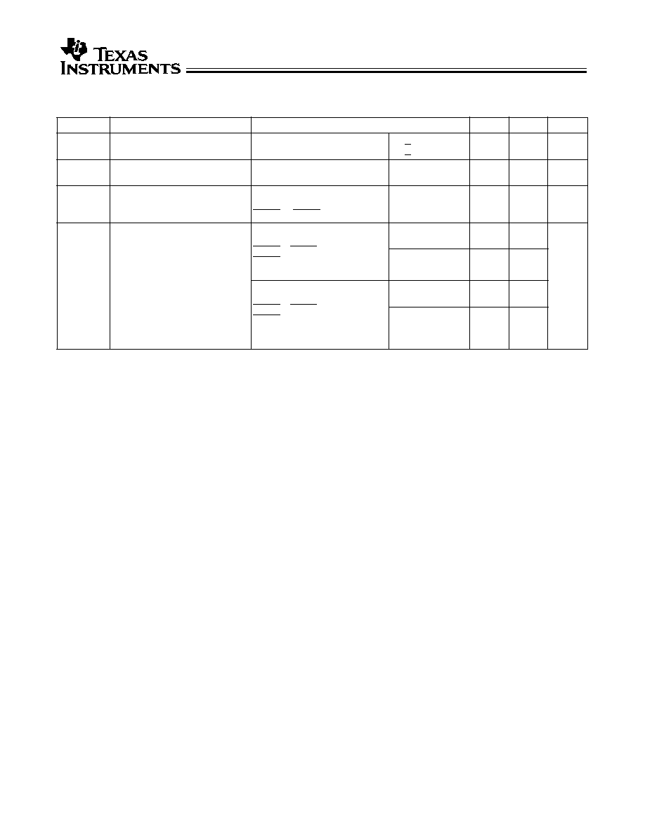
Electrical Characteristics
Over the Operating Range
Parameter
Description
Test Conditions
Min.
Typ.
[7]
Max.
Unit
V
IH
Input HIGH Voltage
2.0
V
V
IL
Input LOW Voltage
0.8
V
V
H
Input Hysteresis
[8]
100
mV
V
IK
Input Clamp Diode Voltage
V
CC
=Min., I
IN
= ≠18 mA
≠0.7
≠1.2
V
I
IH
Input HIGH Current
Standard
V
CC
=Max., V
I
=V
CC
±
1
µ
A
Bus Hold
±
100
I
IL
Input LOW Current
Standard
V
CC
=Max., V
I
=GND
±
1
µ
A
Bus Hold
±
100
µ
A
I
BBH
I
BBL
Bus Hold Sustain Current on Bus Hold Input
[9]
V
CC
=Min.
V
I
=2.0V
≠50
µ
A
V
I
=0.8V
+50
µ
A
I
BHHO
I
BHLO
Bus Hold Overdrive Current on Bus Hold Input
[9]
V
CC
=Max., V
I
=1.5V
TBD
mA
I
OZH
High Impedance Output Current (Three-State
Output pins)
V
CC
=Max., V
OUT
=2.7V
±
1
µ
A
I
OZL
High Impedance Output Current (Three-State
Output pins)
V
CC
=Max., V
OUT
=0.5V
±
1
µ
A
I
OS
Short Circuit Current
[10]
V
CC
=Max., V
OUT
=GND
≠80
≠140
≠200
mA
I
O
Output Drive Current
[10]
V
CC
=Max., V
OUT
=2.5V
≠50
≠180
mA
I
OFF
Power-Off Disable
V
CC
=0V, V
OUT
4.5V
[11]
±
1
µ
A
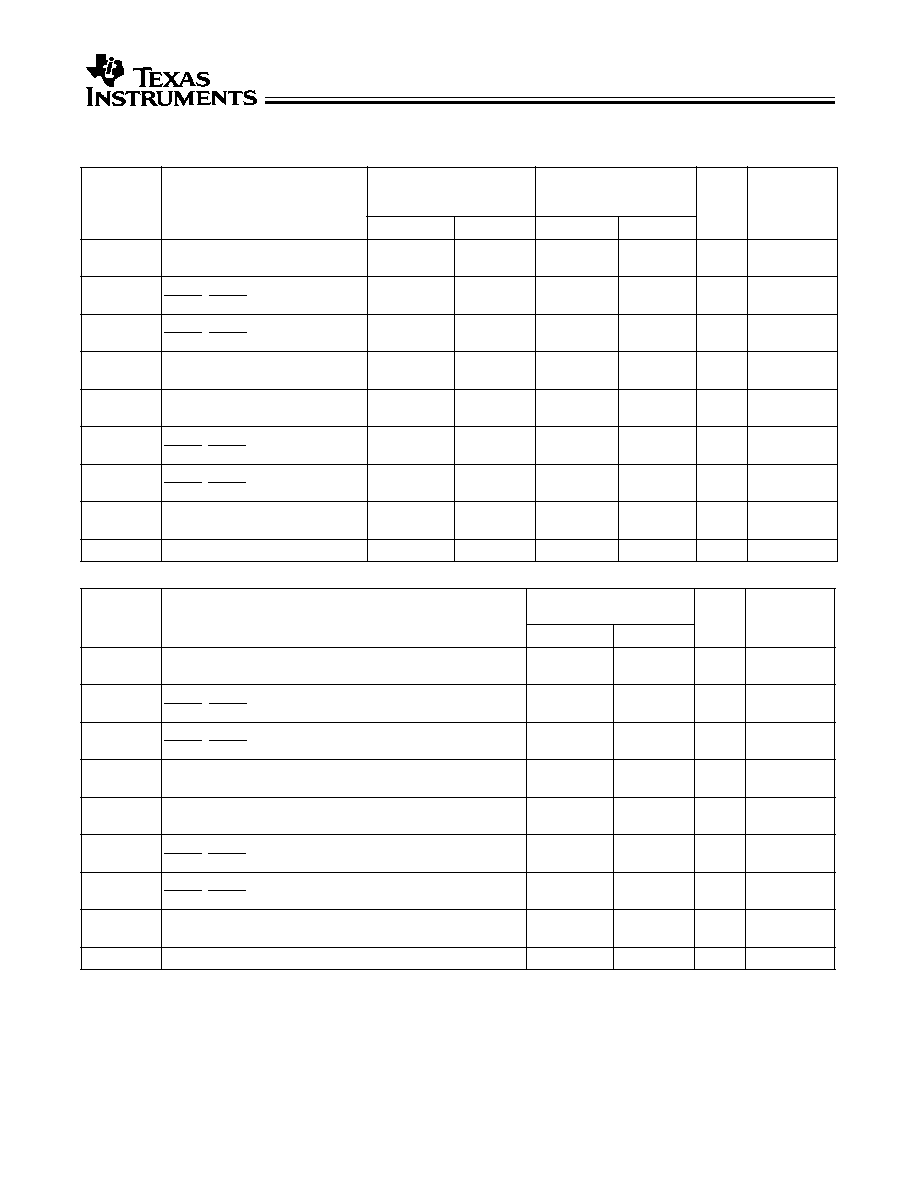
Output Drive Characteristics for CY74FCT16952T
Parameter
Description
Test Conditions
Min.
Typ.
[7]
Max.
Unit
V
OH
Output HIGH Voltage
V
CC
=Min., I
OH
= ≠3 mA
2.5
3.5
V
V
CC
=Min., I
OH
= ≠15 mA
2.4
3.5
V
V
CC
=Min., I
OH
= ≠32 mA
2.0
3.0
V
V
OL
Output LOW Voltage
V
CC
=Min., I
OL
=64 mA
0.2
0.55
V
Output Drive Characteristics for CY74FCT162952T, CY74FCT162H952T
Parameter
Description
Test Conditions
Min.
Typ.
[7]
Max.
Unit
I
ODL
Output LOW Current
[10]
V
CC
=5V, V
IN
=V
IH
or V
IL
, V
OUT
=1.5V
60
115
150
mA
I
ODH
Output HIGH Current
[10]
V
CC
=5V, V
IN
=V
IH
or V
IL
, V
OUT
=1.5V
≠60
≠115
≠150
mA
V
OH
Output HIGH Voltage
V
CC
=Min., I
OH
= ≠24 mA
2.4
3.3
V
V
OL
Output LOW Voltage
V
CC
=Min., I
OL
=24 mA
0.3
0.55
V
Capacitance
[8]
(T
A
= +25∞C, f = 1.0 MHz)
Parameter
Description
Test Conditions
Typ.
[7]
Max.
Unit
C
IN
Input Capacitance
V
IN
= 0V
4.5
6.0
pF
C
OUT
Output Capacitance
V
OUT
= 0V
5.5
8.0
pF
CY74FCT16952T
CY74FCT162952T
CY74FCT162H952T
4
Power Supply Characteristics
Parameter
Description
Test Conditions
[12]
Typ.
[7]
Max.
Unit
I
CC
Quiescent Power Supply Current V
CC
=Max.
V
IN
<0.2V
V
IN
>V
CC
≠0.2V
5
500
µ
A
I
CC
Quiescent Power Supply Current
(TTL inputs HIGH)
V
CC
=Max.
V
IN
=3.4V
[13]
0.5
1.5
mA
I
CCD
Dynamic Power Supply
Current
[14]
V
CC
=Max., One Input Toggling,
50% Duty Cycle, Outputs Open,
OEAB or OEBA=GND
V
IN
=V
CC
or
V
IN
=GND
75
120
µ
A/MHz
I
C
Total Power Supply Current
[15]
V
CC
=Max., F
1
=5 MHz,
F
0
= 10 MHz (CLKAB)
OEAB = CEAB = GND
OEBA = V
CC
50% Duty Cycle,
Outputs Open, One Bit Toggling
V
IN
=V
CC
or
V
IN
=GND
0.8
1.7
mA
V
IN
=3.4V or
V
IN
=GND
1.3
3.2
V
CC
=Max., f
0
=10 MHz (CLKAB)
f
1
=2.5 MHz,
OEAB = CEAB = GND
OEBA = V
CC
50% Duty Cycle,
Outputs Open,
Sixteen Bit Toggling
V
IN
=V
CC
or
V
IN
=GND
3.8
6.5
[16]
V
IN
=3.4V or
V
IN
=GND
8.3
20.0
[16]
Notes:
12. For conditions shown as Max. or Min., use appropriate value specified under Electrical Characteristics for the applicable device type.
13. Per TTL driven input (V
IN
=3.4V); all other inputs at V
CC
or GND.
14. This parameter is not directly testable, but is derived for use in Total Power Supply calculations.
15. I
C
= I
QUIESCENT
+ I
INPUTS
+ I
DYNAMIC
I
C
= I
CC
+
I
CC
D
H
N
T
+I
CCD
(f
0
/2 + f
1
N
1
)
I
CC
= Quiescent Current with CMOS input levels
I
CC
= Power Supply Current for a TTL HIGH input (V
IN
=3.4V)
D
H
= Duty Cycle for TTL inputs HIGH
N
T
= Number of TTL inputs at D
H
I
CCD
= Dynamic Current caused by an input transition pair (HLH or LHL)
f
0
= Clock frequency for registered devices, otherwise zero
f
1
= Input signal frequency
N
1
= Number of inputs changing at f
1
All currents are in milliamps and all frequencies are in megahertz.
16. Values for these conditions are examples of the I
CC
formula. These limits are specified but not tested.
CY74FCT16952T
CY74FCT162952T
CY74FCT162H952T
5
Switching Characteristics
Over the Operating Range
[17]
CY74FCT16952AT
CY74FCT162952AT
CY74FCT162H952AT
CY74FCT162952BT
Parameter
Description
Min.
Max.
Min.
Max.
Unit
Fig. No.
[18]
t
PLH
t
PHL
Propagation Delay
CLKAB, CLKBA to B, A
2.0
10.0
2.0
7.5
ns
1, 5
t
PZH
t
PZL
Output Enable Time
OEBA, OEAB to A, B
1.5
10.5
1.5
8.0
ns
1, 7, 8
t
PHZ
t
PLZ
Output Disable Time
OEBA, OEAB to A, B
1.5
10.0
1.5
7.5
ns
1, 7, 8
t
SU
Set-Up Time, HIGH or LOW
A, B to CLKAB, CLKBA
2.5
--
2.5
--
ns
4
t
H
Hold Time, HIGH or LOW
A, B to CLKAB, CLKBA
2.0
--
1.5
--
ns
4
t
SU
Set-Up Time, HIGH or LOW
CEAB, CEBA to CLKAB, CLKBA
3.0
--
3.0
--
ns
4
t
H
Hold Time, HIGH or LOW
CEAB, CEBA to CLKAB, CLKBA
2.0
--
2.0
--
ns
4
t
W
Pulse Width HIGH or LOW
CLKAB or CLKBA
[19]
3.0
--
3.0
--
ns
5
t
SK(O)
Output Skew
[20]
--
0.5
--
0.5
ns
--
CY74FCT16952CT
CY74FCT162H952CT
Parameter
Description
Min.
Max.
Unit
Fig. No.
[18]
t
PLH
t
PHL
Propagation Delay
CLKAB, CLKBA to B, A
2.0
6.3
ns
1, 5
t
PZH
t
PZL
Output Enable Time
OEBA, OEAB to A, B
1.5
7.0
ns
1, 7, 8
t
PHZ
t
PLZ
Output Disable Time
OEBA, OEAB to A, B
1.5
6.5
ns
1, 7, 8
t
SU
Set-Up Time, HIGH or LOW
A, B to CLKAB, CLKBA
2.5
--
ns
4
t
H
Hold Time, HIGH or LOW
A, B to CLKAB, CLKBA
1.5
--
ns
4
t
SU
Set-Up Time, HIGH or LOW
CEAB, CEBA to CLKAB, CLKBA
3.0
--
ns
4
t
H
Hold Time, HIGH or LOW
CEAB, CEBA to CLKAB, CLKBA
2.0
--
ns
4
t
W
Pulse Width HIGH or LOW
CLKAB or CLKBA
[19]
3.0
--
ns
5
t
SK(O)
Output Skew
[20]
--
0.5
ns
--
Notes:
17. Minimum limits are specified but not tested on Propagation Delays.
18. See "Parameter Measurement Information" in the General Information section.
19. This parameter is specified but not tested.
20. Skew between any two outputs of the same package switching in the same direction. This parameter is ensured by design.
CY74FCT16952T
CY74FCT162952T
CY74FCT162H952T
6
Ordering Information CY74FCT16952
Speed
(ns)
Ordering Code
Package
Name
Package Type
Operating
Range
6.3
CY74FCT16952CTPACT
Z56
56-Lead (240-Mil) TSSOP
Industrial
10.0
CY74FCT16952ATPVC/PVCT
O56
56-Lead (300-Mil) SSOP
Industrial
Ordering Information CY74FCT162952
Speed
(ns)
Ordering Code
Package
Name
Package Type
Operating
Range
7.5
CY74FCT162952BTPVC
O56
56-Lead (300-Mil) SSOP
Industrial
74FCT162952BTPVCT
O56
56-Lead (300-Mil) SSOP
10.0
74FCT162952ATPACT
Z56
56-Lead (240-Mil) TSSOP
Industrial
Ordering Information CY74FCT162H952
Speed
(ns)
Ordering Code
Package
Name
Package Type
Operating
Range
6.3
74FCT162H952CTPVC/PVCT
O56
56-Lead (300-Mil) SSOP
Industrial
10.0
74FCT162H952ATPACT
Z56
56-Lead (240-Mil) TSSOP
Industrial
CY74FCT16952T
CY74FCT162952T
CY74FCT162H952T
7
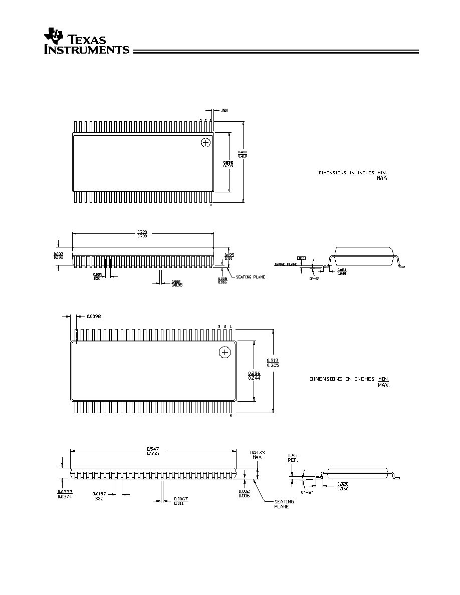
Package Diagrams
56-Lead Shrunk Small Outline Package O56
56-Lead Thin Shrunk Small Outline Package Z56

IMPORTANT NOTICE
Texas Instruments Incorporated and its subsidiaries (TI) reserve the right to make corrections, modifications,
enhancements, improvements, and other changes to its products and services at any time and to discontinue
any product or service without notice. Customers should obtain the latest relevant information before placing
orders and should verify that such information is current and complete. All products are sold subject to TI's terms
and conditions of sale supplied at the time of order acknowledgment.
TI warrants performance of its hardware products to the specifications applicable at the time of sale in
accordance with TI's standard warranty. Testing and other quality control techniques are used to the extent TI
deems necessary to support this warranty. Except where mandated by government requirements, testing of all
parameters of each product is not necessarily performed.
TI assumes no liability for applications assistance or customer product design. Customers are responsible for
their products and applications using TI components. To minimize the risks associated with customer products
and applications, customers should provide adequate design and operating safeguards.
TI does not warrant or represent that any license, either express or implied, is granted under any TI patent right,
copyright, mask work right, or other TI intellectual property right relating to any combination, machine, or process
in which TI products or services are used. Information published by TI regarding third≠party products or services
does not constitute a license from TI to use such products or services or a warranty or endorsement thereof.
Use of such information may require a license from a third party under the patents or other intellectual property
of the third party, or a license from TI under the patents or other intellectual property of TI.
Reproduction of information in TI data books or data sheets is permissible only if reproduction is without
alteration and is accompanied by all associated warranties, conditions, limitations, and notices. Reproduction
of this information with alteration is an unfair and deceptive business practice. TI is not responsible or liable for
such altered documentation.
Resale of TI products or services with statements different from or beyond the parameters stated by TI for that
product or service voids all express and any implied warranties for the associated TI product or service and
is an unfair and deceptive business practice. TI is not responsible or liable for any such statements.
Mailing Address:
Texas Instruments
Post Office Box 655303
Dallas, Texas 75265
Copyright
2001, Texas Instruments Incorporated