Äîêóìåíòàöèÿ è îïèñàíèÿ www.docs.chipfind.ru
SN74GTLP22034
8-BIT LVTTL-TO-GTLP ADJUSTABLE-EDGE-RATE REGISTERED TRANSCEIVER
WITH SPLIT LVTTL PORT AND FEEDBACK PATH
SCES355C JUNE 2001 REVISED SEPTEMBER 2001
1
POST OFFICE BOX 655303
·
DALLAS, TEXAS 75265
D
Member of the Texas Instruments
Widebus
Family
D
TI-OPC
Circuitry Limits Ringing on
Unevenly Loaded Backplanes
D
OEC
Circuitry Improves Signal Integrity
and Reduces Electromagnetic Interference
D
Bidirectional Interface Between GTLP
Signal Levels and LVTTL Logic Levels
D
Split LVTTL Port Provides a Feedback Path
for Control and Diagnostics Monitoring
D
AO Outputs Have Equivalent 26-
Series
Resistors, So No External Resistors Are
Required
D
LVTTL Interfaces Are 5-V Tolerant
D
High-Drive GTLP Open-Drain Outputs
(100 mA)
D
LVTTL Outputs (12 mA/12 mA)
D
Variable Edge-Rate Control (ERC) Input
Selects GTLP Rise and Fall Times for
Optimal Data-Transfer Rate and Signal
Integrity in Distributed Loads
D
I
off
, Power-Up 3-State, and BIAS V
CC
Support Live Insertion
D
Distributed V
CC
and GND Pins Minimize
High-Speed Switching Noise
D
Latch-Up Performance Exceeds 100 mA Per
JESD 78, Class II
D
ESD Protection Exceeds JESD 22
2000-V Human-Body Model (A114-A)
200-V Machine Model (A115-A)
1000-V Charged-Device Model (C101)
description
The SN74GTLP22034 is a high-drive, 8-bit, three-wire registered transceiver that provides true LVTTL-to-GTLP
and GTLP-to-LVTTL signal-level translation. The device allows for transparent, latched, and flip-flop modes of
data transfer with separate LVTTL input and LVTTL output pins, which provides a feedback path for control and
diagnostics monitoring, the same functionality as the SN74FB2033, but with true logic. The device provides a
high-speed interface between cards operating at LVTTL logic levels and a backplane operating at GTLP signal
levels. High-speed (about three times faster than standard LVTTL or TTL) backplane operation is a direct result
of GTLP's reduced output swing (
<
1 V), reduced input threshold levels, improved differential input, OEC
circuitry, and TI-OPC
circuitry. Improved GTLP OEC and TI-OPC circuits minimize bus-settling time and have
been designed and tested using several backplane models. The high drive allows incident-wave switching in
heavily loaded backplanes with equivalent load impedance down to 11
.
The AO outputs, which are designed to sink up to 12 mA, include equivalent 26-
resistors to reduce overshoot
and undershoot.
Copyright
2001, Texas Instruments Incorporated
Please be aware that an important notice concerning availability, standard warranty, and use in critical applications of
Texas Instruments semiconductor products and disclaimers thereto appears at the end of this data sheet.
OEC, TI-OPC, and Widebus are trademarks of Texas Instruments.
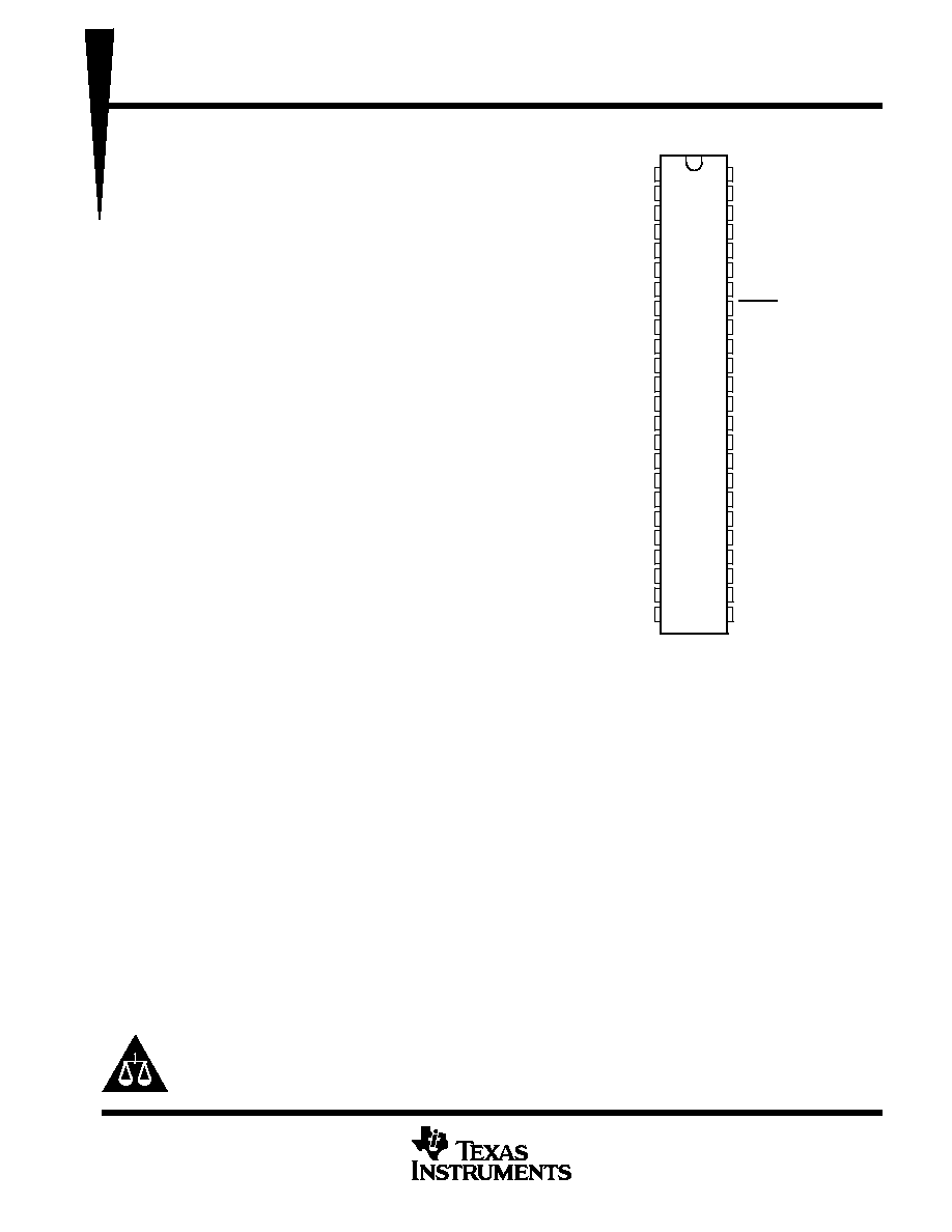
DGG OR DGV PACKAGE
(TOP VIEW)
1
2
3
4
5
6
7
8
9
10
11
12
13
14
15
16
17
18
19
20
21
22
23
24
48
47
46
45
44
43
42
41
40
39
38
37
36
35
34
33
32
31
30
29
28
27
26
25
IMODE1
AI1
AO1
GND
AI2
AO2
V
CC
AI3
AO3
GND
AI4
AO4
AO5
AI5
GND
AO6
AI6
V
CC
AO7
AI7
GND
AO8
AI8
OMODE0
IMODE0
BIAS V
CC
B1
GND
OEAB
B2
ERC
OEAB
B3
GND
CLKAB/LEAB
B4
B5
CLKBA/LEBA
GND
B6
OEBA
V
CC
B7
LOOPBACK
GND
B8
V
REF
OMODE1
PRODUCTION DATA information is current as of publication date.
Products conform to specifications per the terms of Texas Instruments
standard warranty. Production processing does not necessarily include
testing of all parameters.
SN74GTLP22034
8-BIT LVTTL-TO-GTLP ADJUSTABLE-EDGE-RATE REGISTERED TRANSCEIVER
WITH SPLIT LVTTL PORT AND FEEDBACK PATH
SCES355C JUNE 2001 REVISED SEPTEMBER 2001
2
POST OFFICE BOX 655303
·
DALLAS, TEXAS 75265
description (continued)
GTLP is the Texas Instruments derivative of the Gunning Transceiver Logic (GTL) JEDEC standard JESD 8-3.
The ac specification of the SN74GTLP22034 is given only at the preferred higher noise-margin GTLP, but the
user has the flexibility of using this device at either GTL (V
TT
= 1.2 V and V
REF
= 0.8 V) or GTLP (V
TT
= 1.5 V
and V
REF
= 1 V) signal levels. For information on using GTLP devices in FB+/BTL applications, refer to TI
application reports, Texas Instruments GTLP Frequently Asked Questions,
literature number SCEA019, and
GTLP in BTL Applications, literature number SCEA017.
Normally, the B port operates at GTLP signal levels. The A-port and control inputs operate at LVTTL logic levels,
but are 5-V tolerant and can be directly driven by TTL or 5-V CMOS devices. V
REF
is the B-port differential input
reference voltage.
This device is fully specified for live-insertion applications using I
off
, power-up 3-state, and BIAS V
CC
. The I
off
circuitry disables the outputs, preventing damaging current backflow through the device when it is powered
down. The power-up 3-state circuitry places the outputs in the high-impedance state during power up and power
down, which prevents driver conflict. The BIAS V
CC
circuitry precharges and preconditions the B-port
input/output connections, preventing disturbance of active data on the backplane during card insertion or
removal, and permits true live-insertion capability.
This GTLP device features TI-OPC circuitry, which actively limits overshoot caused by improperly terminated
backplanes, unevenly distributed cards, or empty slots during low-to-high signal transitions. This improves
signal integrity, which allows adequate noise margin to be maintained at higher frequencies.
High-drive GTLP backplane interface devices feature adjustable edge-rate control (ERC). Changing the ERC
input voltage between low and high adjusts the B-port output rise and fall times.
This allows the designer to
optimize system data-transfer rate and signal integrity to the backplane load.
When V
CC
is between 0 and 1.5 V, the device is in the high-impedance state during power up or power down.
However, to ensure the high-impedance state above 1.5 V, OEAB should be tied to V
CC
through a pullup resistor
and OEAB and OEBA should be tied to GND through a pulldown resistor; the minimum value of the resistor is
determined by the current-sinking/current-sourcing capability of the driver.
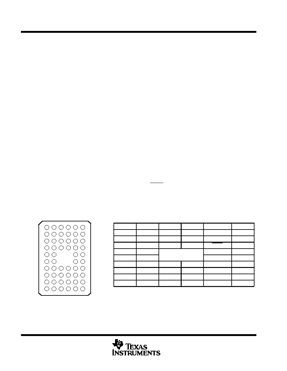
terminal assignments
1
2
3
4
5
6
A
IMODE1
NC
NC
NC
NC
IMODE0
B
AO1
AI1
GND
GND
BIAS VCC
B1
C
AO2
AI2
VCC
ERC
OEAB
B2
D
AO3
AI3
GND
GND
OEAB
B3
E
AO4
AI4
CLKAB/LEAB
B4
F
AO5
AI5
CLKBA/LEBA
B5
G
AO6
AI6
GND
GND
OEBA
B6
H
AO7
AI7
VCC
VCC
LOOPBACK
B7
J
AO8
AI8
GND
GND
VREF
B8
K
OMODE0
NC
NC
NC
NC
OMODE1
NC = No internal connection
GQL PACKAGE
(TOP VIEW)
A
B
C
D
E
F
G
H
J
K
1
2
3
4
5
6
SN74GTLP22034
8-BIT LVTTL-TO-GTLP ADJUSTABLE-EDGE-RATE REGISTERED TRANSCEIVER
WITH SPLIT LVTTL PORT AND FEEDBACK PATH
SCES355C JUNE 2001 REVISED SEPTEMBER 2001
3
POST OFFICE BOX 655303
·
DALLAS, TEXAS 75265
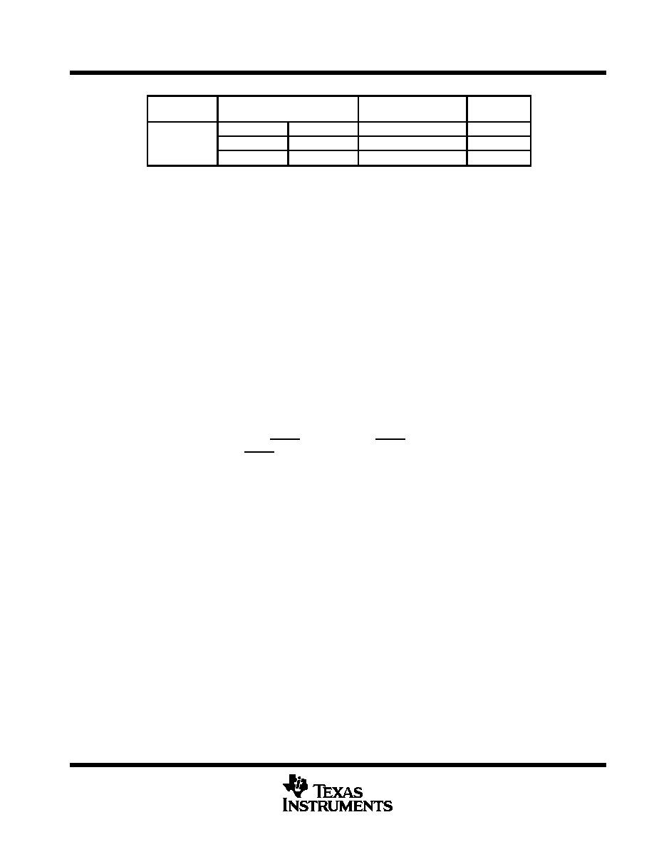
ORDERING INFORMATION
TA
PACKAGE
ORDERABLE
PART NUMBER
TOP-SIDE
MARKING
TSSOP DGG
Tape and reel
SN74GTLP22034DGGR
GTLP22034
40
°
C to 85
°
C
TVSOP DGV
Tape and reel
SN74GTLP22034DGVR
GT22034
VFBGA GQL
Tape and reel
SN74GTLP22034GQLR
GS034
Package drawings, standard packing quantities, thermal data, symbolization, and PCB design
guidelines are available at www.ti.com/sc/package.
functional description
The SN74GTLP22034 is a high-drive (100 mA), 8-bit, three-wire registered transceiver containing D-type
latches and D-type flip-flops for data-path operation in the transparent, latched, or flip-flop modes. Data
transmission is true, with AI data going to the B port and B data going to AO. The split LVTTL AI and AO provides
a feedback path for control and diagnostics monitoring.
The logic element for data flow in each direction is configured by two mode (IMODE1 and IMODE0 for B to A,
OMODE1 and OMODE0 for A to B) inputs as a buffer, a D-type flip-flop, or a D-type latch. When configured in
the buffer mode, the input data appears at the output port. In the flip-flop mode, data is stored on the rising edge
of the appropriate clock (CLKAB/LEAB or CLKBA/LEBA) input. In the latch mode, the clock inputs serve as
active-high transparent latch enables.
Data flow in the B-to-A direction, regardless of the logic element selected, is further controlled by the
LOOPBACK input. When LOOPBACK is low, B-port data is the B-to-A input. When LOOPBACK is high, the
output of the selected A-to-B logic element is the B-to-A input.
The AO enable/disable control is provided by OEBA. When OEBA is low or when V
CC
is less than 1.5 V, AO
is in the high-impedance state. When OEBA is high, AO is active (high or low logic levels).
The B port is controlled by OEAB and OEAB. If OEAB is low, OEAB is high, or V
CC
is less than 1.5 V, the B port
is inactive. If OEAB is high and OEAB is low, the B port is active.
The A-to-B and B-to-A logic elements are active, regardless of the state of their associated outputs. The logic
elements can enter new data (in flip-flop and latch modes) or retain previously stored data while the associated
outputs are in the high-impedance (AO) or inactive (B port) states.
SN74GTLP22034
8-BIT LVTTL-TO-GTLP ADJUSTABLE-EDGE-RATE REGISTERED TRANSCEIVER
WITH SPLIT LVTTL PORT AND FEEDBACK PATH
SCES355C JUNE 2001 REVISED SEPTEMBER 2001
4
POST OFFICE BOX 655303
·
DALLAS, TEXAS 75265
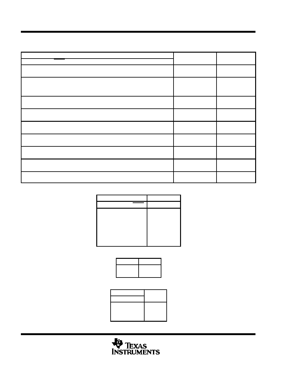
Function Tables
FUNCTION/MODE
INPUTS
OUTPUT
MODE
OEBA
OEAB
OEAB
OMODE1
OMODE0
IMODE1
IMODE0
LOOPBACK
OUTPUT
MODE
L
L
X
X
X
X
X
X
Z
Isolation
L
X
H
X
X
X
X
X
Z
Isolation
X
H
L
L
L
X
X
X
Buffer
X
H
L
L
H
X
X
X
AI to B
Flip-flop
X
H
L
H
X
X
X
X
Latch
H
L
X
X
X
L
L
L
B t AO
B ff
H
X
H
X
X
L
L
L
B to AO
Buffer
H
L
X
X
X
L
H
L
B t AO
Fli fl
H
X
H
X
X
L
H
L
B to AO
Flip-flop
H
L
X
X
X
H
X
L
B t AO
L t h
H
X
H
X
X
H
X
L
B to AO
Latch
H
L
X
X
X
L
L
H
AI to AO
Buffer
H
X
H
X
X
L
L
H
AI to AO
Buffer
H
L
X
X
X
L
H
H
AI to AO
Flip flop
H
X
H
X
X
L
H
H
AI to AO
Flip-flop
H
L
X
X
X
H
X
H
AI to AO
Latch
H
X
H
X
X
H
X
H
AI to AO
Latch
H
H
L
X
X
X
X
L
AI to B, B to AO
Transparent with
feedback path
ENABLE/DISABLE
INPUTS
OUTPUTS
OEBA
OEAB
OEAB
AO
B
L
X
X
Z
H
X
X
Active
X
L
L
Z
X
L
H
Z
X
H
L
Active
X
H
H
Z
BUFFER
INPUT
OUTPUT
L
L
H
H
LATCH
INPUTS
OUTPUT
CLK/LE
DATA
OUTPUT
H
L
L
H
H
H
L
X
Q0
SN74GTLP22034
8-BIT LVTTL-TO-GTLP ADJUSTABLE-EDGE-RATE REGISTERED TRANSCEIVER
WITH SPLIT LVTTL PORT AND FEEDBACK PATH
SCES355C JUNE 2001 REVISED SEPTEMBER 2001
5
POST OFFICE BOX 655303
·
DALLAS, TEXAS 75265
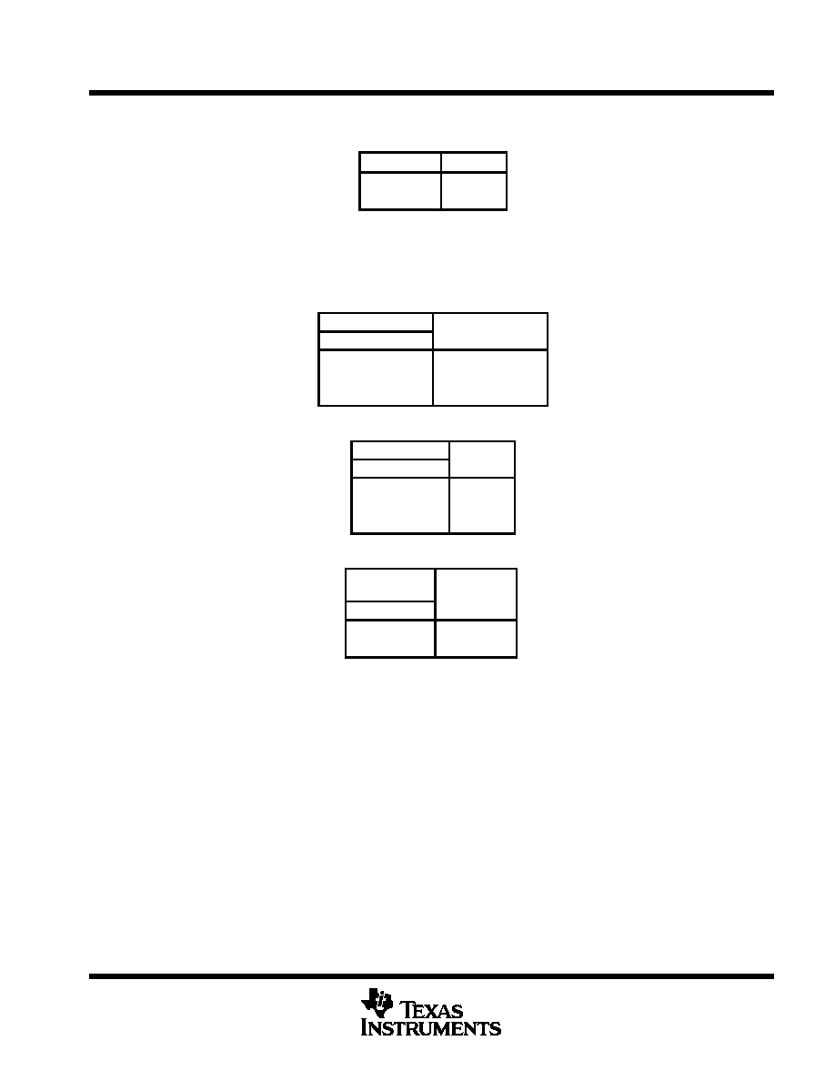
Function Tables (Continued)
LOOPBACK
LOOPBACK
Q
L
B port
H
Point P
Q is the input to the B-to-A
logic element.
P is the output of the A-to-B
logic element (see functional
block diagram).
SELECT
INPUTS
SELECTED LOGIC
MODE1
MODE0
ELEMENT
L
L
Buffer
L
H
Flip-flop
H
X
Latch
FLIP-FLOP
INPUTS
OUTPUT
CLK/ LE
DATA
OUTPUT
L
X
Q0
L
L
H
H
B-PORT EDGE-RATE CONTROL (ERC)
INPUT
ERC
OUTPUT
B-PORT
LOGIC LEVEL
EDGE RATE
H
Slow
L
Fast