SN74LV161284
19-BIT BUS INTERFACE
SCLS426C ≠ OCTOBER 1998 ≠ REVISED NOVEMBER 2002
1
POST OFFICE BOX 655303
∑
DALLAS, TEXAS 75265
D
4.5-V to 5.5-V V
CC
Operation
D
1.4-k
Pullup Resistors Integrated on All
Open-Drain Outputs Eliminate the Need for
Discrete Resistors
D
Designed for IEEE Std 1284-I (Level-1 Type)
and IEEE Std 1284-II (Level-2 Type)
Electrical Specifications
D
Flow-Through Architecture Optimizes PCB
Layout
D
Latch-Up Performance Exceeds 250 mA Per
JEDEC 17
D
ESD Protection Exceeds JESD 22
≠ 4000-V Human-Body Model (A114-A)
≠ 300-V Machine Model (A115-A)
≠ 2000-V Charged-Device Model (C101)
description/ordering information
The SN74LV161284 is designed for 4.5-V to
5.5-V V
CC
operation. This device provides
asynchronous two-way communication between
data buses. The control-function implementation
minimizes external timing requirements.
This device has eight bidirectional bits; data can
flow in the A-to-B direction when DIR is high, and
in the B-to-A direction when DIR is low. This
device also has five drivers, which drive the cable
side, and four receivers. The SN74LV161284 has
one receiver dedicated to the HOST LOGIC line
and a driver to drive the PERI LOGIC line.
The output drive mode is determined by the high-drive (HD) control pin. When HD is high, the B, Y, and
PERI LOGIC OUT outputs are in a totem-pole configuration, and in an open-drain configuration when HD is low.
This meets the drive requirements as specified in the IEEE Std 1284-I (level-1 type) and IEEE Std 1284-II
(level-2 type) parallel peripheral-interface specifications. Except for HOST LOGIC IN and PERI LOGIC OUT,
all cable-side pins have a 1.4-k
integrated pullup resistor. The pullup resistor is switched off if the associated
output driver is in the low state or if the output voltage is above V
CC
CABLE. If V
CC
CABLE is off,
PERI LOGIC OUT is set to low.
The device has two supply voltages. V
CC
is designed for 4.5-V to 5.5-V operation. V
CC
CABLE supplies the
output buffers of the cable side only and is designed for 4.5-V to 5.5-V operation.
ORDERING INFORMATION
TA
PACKAGE
ORDERABLE
PART NUMBER
TOP-SIDE
MARKING
SSOP
DL
Tube
SN74LV161284DL
LV161284
≠40
∞
C to 85
∞
C
SSOP ≠ DL
Tape and reel
SN74LV161284DLR
LV161284
TSSOP ≠ DGG
Tape and reel
SN74LV161284DGGR
LV161284
Package drawings, standard packing quantities, thermal data, symbolization, and PCB design guidelines are
available at www.ti.com/sc/package.
Copyright
2002, Texas Instruments Incorporated
PRODUCTION DATA information is current as of publication date.
Products conform to specifications per the terms of Texas Instruments
standard warranty. Production processing does not necessarily include
testing of all parameters.
Please be aware that an important notice concerning availability, standard warranty, and use in critical applications of
Texas Instruments semiconductor products and disclaimers thereto appears at the end of this data sheet.
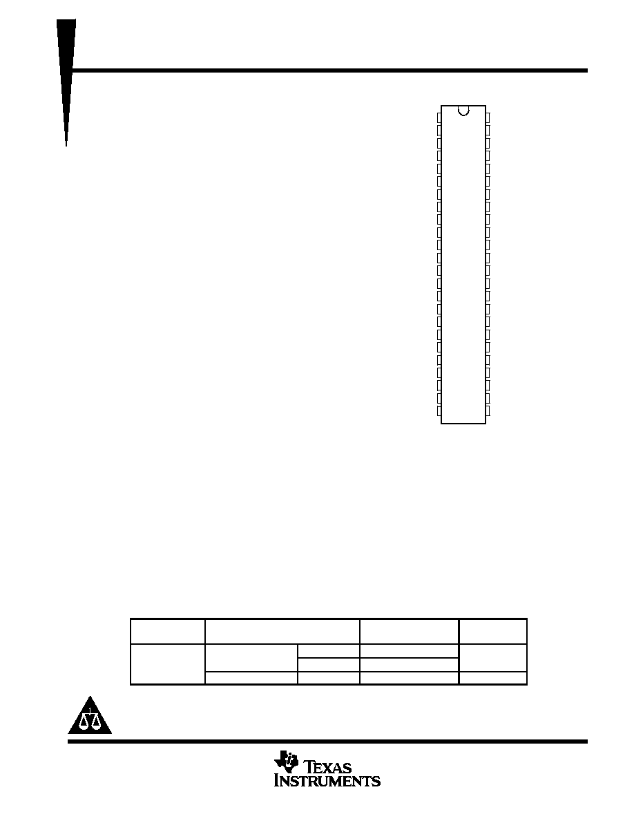
DGG OR DL PACKAGE
(TOP VIEW)
1
2
3
4
5
6
7
8
9
10
11
12
13
14
15
16
17
18
19
20
21
22
23
24
48
47
46
45
44
43
42
41
40
39
38
37
36
35
34
33
32
31
30
29
28
27
26
25
HD
A9
A10
A11
A12
A13
V
CC
A1
A2
GND
A3
A4
A5
A6
GND
A7
A8
V
CC
PERI LOGIC IN
A14
A15
A16
A17
HOST LOGIC OUT
DIR
Y9
Y10
Y11
Y12
Y13
V
CC
CABLE
B1
B2
GND
B3
B4
B5
B6
GND
B7
B8
V
CC
CABLE
PERI LOGIC OUT
C14
C15
C16
C17
HOST LOGIC IN
SN74LV161284
19-BIT BUS INTERFACE
SCLS426C ≠ OCTOBER 1998 ≠ REVISED NOVEMBER 2002
2
POST OFFICE BOX 655303
∑
DALLAS, TEXAS 75265
FUNCTION TABLE
INPUTS
OUTPUT
MODE
DIR
HD
OUTPUT
MODE
L
L
Open drain
A9≠A13 to Y9≠Y13 and PERI LOGIC IN to PERI LOGIC OUT
L
L
Totem pole
B1≠B8 to A1≠A8 and C14≠C17 to A14≠A17
L
H
Totem pole
B1≠B8 to A1≠A8, A9≠A13 to Y9≠Y13, PERI LOGIC IN to PERI LOGIC OUT, and C14≠C17 to A14≠A17
H
L
Open drain
A1≠A8 to B1≠B8, A9≠A13 to Y9≠Y13, and PERI LOGIC IN to PERI LOGIC OUT
H
L
Totem pole
C14≠C17 to A14≠A17
H
H
Totem pole
A1≠A8 to B1≠B8, A9≠A13 to Y9≠Y13, C14≠C17 to A14≠A17, and PERI LOGIC IN to PERI LOGIC OUT
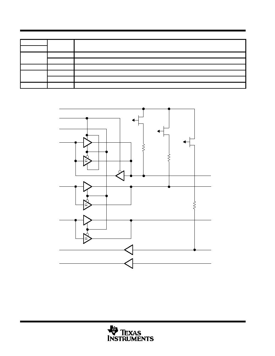
logic diagram (positive logic)
See Note B
See Note B
See Note A
B1≠B8
Y9≠Y13
PERI LOGIC OUT
C14≠C17
HOST LOGIC IN
VCC CABLE
DIR
HD
A1≠A8
A9≠A13
PERI LOGIC IN
A14≠A17
HOST LOGIC OUT
42
48
1
19
24
30
25
NOTES: A. The PMOS prevents backdriving current from the signal pins to VCC CABLE when VCC CABLE is open or at GND.
B. The PMOS prevents backdriving current from the signal pins to VCC CABLE when VCC CABLE is open or at GND. The PMOS
is turned off when the associated driver is in the low state.
SN74LV161284
19-BIT BUS INTERFACE
SCLS426C ≠ OCTOBER 1998 ≠ REVISED NOVEMBER 2002
3
POST OFFICE BOX 655303
∑
DALLAS, TEXAS 75265
absolute maximum ratings over operating free-air temperature range (unless otherwise noted)
Supply voltage range: V
CC
CABLE
≠0.5 V to 7 V
. . . . . . . . . . . . . . . . . . . . . . . . . . . . . . . . . . . . . . . . . . . . . . . . . .
V
CC
≠0.5 V to 7 V
. . . . . . . . . . . . . . . . . . . . . . . . . . . . . . . . . . . . . . . . . . . . . . . . . . . . . . . . .
Input and output voltage range, V
I
and V
O
: Cable side (see Notes 1 and 2)
≠2 V to 7 V
. . . . . . . . . . . . . . . . . .
Peripheral side (see Note 1)
≠0.5 V to V
CC
+ 0.5 V
. . . . . . . . . . .
Input clamp current, I
IK
(V
I
< 0 or V
I
> V
CC
)
±
20 mA
. . . . . . . . . . . . . . . . . . . . . . . . . . . . . . . . . . . . . . . . . . . . . . .
Output clamp current, I
OK
(V
O
< 0 or V
O
> V
CC
)
±
50 mA
. . . . . . . . . . . . . . . . . . . . . . . . . . . . . . . . . . . . . . . . . . . .
Continuous output current, I
O
(V
O
= 0 to V
CC
)
±
50 mA
. . . . . . . . . . . . . . . . . . . . . . . . . . . . . . . . . . . . . . . . . . . . . .
Continuous current through each V
CC
or GND
±
200 mA
. . . . . . . . . . . . . . . . . . . . . . . . . . . . . . . . . . . . . . . . . . . . .
Output high sink current, I
SK
(V
O
= 5.5 V and V
CC
CABLE = 5.5 V)
65 mA
. . . . . . . . . . . . . . . . . . . . . . . . . . . .
Package thermal impedance,
JA
(see Note 3): DGG package
70
∞
C/W
. . . . . . . . . . . . . . . . . . . . . . . . . . . . . . .
DL package
63
∞
C/W
. . . . . . . . . . . . . . . . . . . . . . . . . . . . . . . . .
Storage temperature range, T
stg
≠65
∞
C to 150
∞
C
. . . . . . . . . . . . . . . . . . . . . . . . . . . . . . . . . . . . . . . . . . . . . . . . . . .
Stresses beyond those listed under "absolute maximum ratings" may cause permanent damage to the device. These are stress ratings only, and
functional operation of the device at these or any other conditions beyond those indicated under "recommended operating conditions" is not
implied. Exposure to absolute-maximum-rated conditions for extended periods may affect device reliability.
NOTES:
1. The input and output voltage ratings may be exceeded if the input and output current ratings are observed.
2. The ac input voltage pulse duration is limited to 40 ns if the amplitude is more negative than ≠0.5 V.
3. The package thermal impedance is calculated in accordance with JESD 51-7.
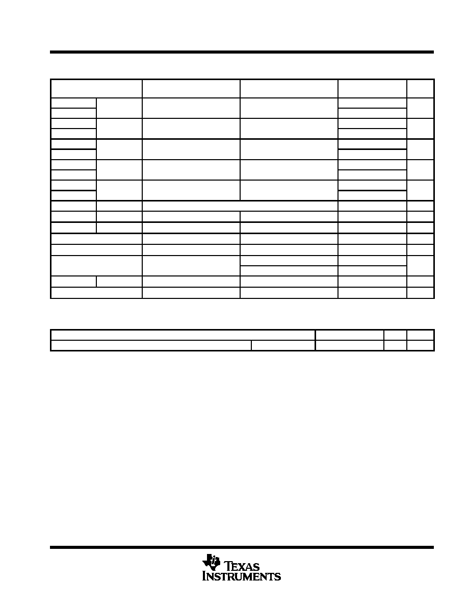
recommended operating conditions (see Note 4)
MIN
MAX
UNIT
VCC CABLE
Supply voltage for the cable side, VCC CABLE
VCC
4.5
5.5
V
VCC
Supply voltage
4.5
5.5
V
A, DIR, HD, and PERI LOGIC IN
VCC
◊
0.7
VIH
High level input voltage
B
2
V
VIH
High-level input voltage
C14≠C17
2.3
V
HOST LOGIC IN
2.6
A, DIR, HD, and PERI LOGIC IN
VCC
◊
0.3
VIL
Low level input voltage
B
0.8
V
VIL
Low-level input voltage
C14≠C17
0.8
V
HOST LOGIC IN
1.6
VI
Input voltage
Peripheral side
0
VCC
V
VI
Input voltage
Cable side
0
5.5
V
VO
Open-drain output voltage
B, Y, and PERI LOGIC OUT (HD low)
0
5.5
V
B and Y outputs (HD high)
≠14
IOH
High-level output current
A outputs and HOST LOGIC OUT
≠8
mA
PERI LOGIC OUT
≠0.5
B and Y outputs
14
IOL
Low-level output current
A outputs and HOST LOGIC OUT
8
mA
PERI LOGIC OUT
84
TA
Operating free-air temperature
≠40
85
∞
C
NOTE 4: All unused inputs of the device must be held at VCC or GND to ensure proper device operation. Refer to the TI application report,
Implications of Slow or Floating CMOS Inputs, literature number SCBA004.
SN74LV161284
19-BIT BUS INTERFACE
SCLS426C ≠ OCTOBER 1998 ≠ REVISED NOVEMBER 2002
4
POST OFFICE BOX 655303
∑
DALLAS, TEXAS 75265
electrical characteristics over recommended operating free-air temperature range,
V
CC
CABLE = V
CC
(unless otherwise noted)
PARAMETER
TEST CONDITIONS
VCC
MIN
TYP
MAX
UNIT
V
I
t h
t
i
VthH ≠ VthL for all inputs except the
C inputs and HOST LOGIC IN
4.5 V to 5.5 V
0.4
V
Vt
Input hysteresis
VthH ≠ VthL for the HOST LOGIC IN
5 V
0.3
V
VthH ≠ VthL for the C inputs
5 V
0.8
VIK
Input clamp diode voltage
II = ≠18 mA
3 V
≠1.2
V
B and Y outputs
IOH = ≠14 mA (HD high)
3.73
VOH
A outputs and HOST LOGIC OUT
IOH = ≠8 mA (HD high)
4.5 V
3.8
V
VOH
A outputs and HOST LOGIC OUT
IOH = ≠50
µ
A
4.4
V
PERI LOGIC OUT
IOH = ≠0.5 mA
4.5 V
4.45
B and Y outputs
IOL = 14 mA
0.77
VOL
A outputs and HOST LOGIC OUT
IOL = 50
µ
A
4 5 V
0.1
V
VOL
A outputs and HOST LOGIC OUT
IOL = 8 mA
4.5 V
0.44
V
PERI LOGIC OUT
IOL = 84 mA
0.7
C inputs
VI = VCC
5 5 V
350
µ
A
II
C inputs
VI = GND (pullup resistors)
5.5 V
≠5
mA
II
B and C inputs
VI = 5.5 V or GND
0 to 5.5 V
±
5
mA
All inputs except the B or C inputs
VI = VCC or GND
5.5 V
±
1
µ
A
B outputs
VO = VCC
5.5 V
350
µ
A
IOZ
B outputs
VO = GND (pullup resistors)
5.5 V
≠5
mA
IOZ
A1≠A8
VO = VCC or GND
5.5 V
±
20
µ
A
Open-drain Y outputs
VO = GND (pullup resistors)
5.5 V
≠5
mA
IOZPU
B and Y outputs
VO = 5.5 V
0 to 2 V
350
µ
A
IOZPU
B and Y outputs
VO = GND
0 to 2 V
≠5
mA
IOZPD
B and Y outputs
VO = 5.5 V
2 V to 0
350
µ
A
IOZPD
B and Y outputs
VO = GND
2 V to 0
≠5
mA
I ff
Power-down output leakage,
Outputs B1 ≠ B8, Y9 ≠ Y13, and
PERI LOGIC OUT
VO = 5.5 V
0
100
µ
A
Ioff
Power-down input leakage,
Inputs C14 ≠ C17 and HOST
LOGIC IN
VI = 5.5 V
0
100
µ
A
I
VI = VCC,
IO = 0
5 5 V
0.8
mA
ICC
VI = GND (12
◊
pullup)
5.5 V
70
mA
Ci
All inputs
VI = VCC or GND
5 V
5
pF
Cio
I/O ports
VO = VCC or GND
5 V
9
pF
ZO
Cable side
IOH = ≠35 mA
5 V
45
R pullup
Cable side
VO = 0 V (in Hi Z)
5 V
1.15
1.65
k
All typical values are at VCC = 5 V, TA = 25
∞
C.
A maximum current of 170
µ
A per pin is added to ICC if the pullup resistor pin is above VCC.
SN74LV161284
19-BIT BUS INTERFACE
SCLS426C ≠ OCTOBER 1998 ≠ REVISED NOVEMBER 2002
5
POST OFFICE BOX 655303
∑
DALLAS, TEXAS 75265
switching characteristics over recommended ranges of supply voltage and operating free-air
temperature (unless otherwise noted) (see Figures 1 and 2)
PARAMETER
FROM
(INPUT)
TO
(OUTPUT)
MIN
TYP
MAX
UNIT
tPLH
Totem pole
A or B
B or A
2
30
ns
tPHL
Totem pole
A or B
B or A
2
30
ns
tPLH
Totem pole
A
Y
2
30
ns
tPHL
Totem pole
A
Y
2
30
ns
tPLH
Totem pole
C
A
2
30
ns
tPHL
Totem pole
C
A
2
30
ns
tPLH
Totem pole
PERI LOGIC IN
PERI LOGIC OUT
2
30
ns
tPHL
Totem pole
PERI LOGIC IN
PERI LOGIC OUT
2
30
ns
tPLH
Totem pole
HOST LOGIC IN
HOST LOGIC OUT
2
30
ns
tPHL
Totem pole
HOST LOGIC IN
HOST LOGIC OUT
2
30
ns
tslew
Totem pole
Cable-side outputs
0.05
0.95
V/ns
ten
Totem pole
HD
B, Y, and PERI LOGIC OUT
2
25
ns
tdis
Totem pole
HD
B, Y, and PERI LOGIC OUT
2
25
ns
ten≠tdis
10
ns
ten
DIR
A
2
25
ns
tdi
DIR
A
2
15
ns
tdis
DIR
B
2
25
ns
tr, tf
Open drain
A
B or Y
30
ns
tsk(o)
A or B
B or A
1
6
ns
Skew is measured at 1/2 (VOH + VOL) for signals switching in the same direction.
operating characteristics, V
CC
= 5 V, T
A
= 25
∞
C
PARAMETER
TEST CONDITIONS
TYP
UNIT
Cpd
Power dissipation capacitance
Outputs enabled
CL = 0,
f = 10 MHz
25
pF