Äîêóìåíòàöèÿ è îïèñàíèÿ www.docs.chipfind.ru
SN54LVTH162244, SN74LVTH162244
3.3 V ABT 16 BIT BUFFERS/DRIVERS
WITH 3 STATE OUTPUTS
SCBS258M - JUNE 1993 - REVISED SEPTEMBER 2003
1
POST OFFICE BOX 655303
·
DALLAS, TEXAS 75265
D
Members of the Texas Instruments
Widebus
Family
D
Output Ports Have Equivalent 22-
Series
Resistors, So No External Resistors Are
Required
D
Support Mixed-Mode Signal Operation
(5-V Input and Output Voltages With
3.3-V V
CC
)
D
Support Unregulated Battery Operation
Down to 2.7 V
D
Typical V
OLP
(Output Ground Bounce)
<0.8 V at V
CC
= 3.3 V, T
A
= 25
°
C
D
I
off
and Power-Up 3-State Support Hot
Insertion
D
Bus Hold on Data Inputs Eliminates the
Need for External Pullup/Pulldown
Resistors
D
Distributed V
CC
and GND Pins Minimize
High-Speed Switching Noise
D
Flow-Through Architecture Optimizes PCB
Layout
D
Latch-Up Performance Exceeds 500 mA Per
JESD 17
D
ESD Protection Exceeds JESD 22
- 2000-V Human-Body Model (A114-A)
- 200-V Machine Model (A115-A)
description/ordering information
The 'LVTH162244 devices are 16-bit buffers and line drivers designed for low-voltage (3.3-V) V
CC
operation,
but with the capability to provide a TTL interface to a 5-V system environment. These devices can be used as
four 4-bit buffers, two 8-bit buffers, or one 16-bit buffer. These devices provide true outputs and symmetrical
active-low output-enable (OE) inputs.
ORDERING INFORMATION
TA
PACKAGE
ORDERABLE
PART NUMBER
TOP-SIDE MARKING
SSOP - DL
Tube
SN74LVTH162244DL
LVTH162244
SSOP - DL
Tape and reel
SN74LVTH162244DLR
LVTH162244
-40
°
C to 85
°
C
TSSOP - DGG
Tape and reel
SN74LVTH162244DGGR
LVTH162244
-40 C to 85 C
VFBGA - GQL
Tape and reel
SN74LVTH162244KR
LL2244
VFBGA - ZQL (Pb-free)
Tape and reel
74LVTH162244ZQLR
LL2244
-55
°
C to 125
°
C
CFP - WD
Tube
SNJ54LVTH162244WD
SNJ54LVTH162244WD
Package drawings, standard packing quantities, thermal data, symbolization, and PCB design guidelines are available at
www.ti.com/sc/package.
Copyright
2003, Texas Instruments Incorporated
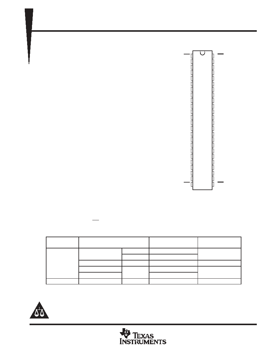
SN54LVTH162244 . . . WD PACKAGE
SN74LVTH162244 . . . DGG OR DL PACKAGE
(TOP VIEW)
1
2
3
4
5
6
7
8
9
10
11
12
13
14
15
16
17
18
19
20
21
22
23
24
48
47
46
45
44
43
42
41
40
39
38
37
36
35
34
33
32
31
30
29
28
27
26
25
1OE
1Y1
1Y2
GND
1Y3
1Y4
V
CC
2Y1
2Y2
GND
2Y3
2Y4
3Y1
3Y2
GND
3Y3
3Y4
V
CC
4Y1
4Y2
GND
4Y3
4Y4
4OE
2OE
1A1
1A2
GND
1A3
1A4
V
CC
2A1
2A2
GND
2A3
2A4
3A1
3A2
GND
3A3
3A4
V
CC
4A1
4A2
GND
4A3
4A4
3OE
Widebus is a trademark of Texas Instruments.
On products compliant to MIL PRF 38535, all parameters are tested
unless otherwise noted. On all other products, production
processing does not necessarily include testing of all parameters.
PRODUCTION DATA information is current as of publication date.
Products conform to specifications per the terms of Texas Instruments
standard warranty. Production processing does not necessarily include
testing of all parameters.
Please be aware that an important notice concerning availability, standard warranty, and use in critical applications of
Texas Instruments semiconductor products and disclaimers thereto appears at the end of this data sheet.
SN54LVTH162244, SN74LVTH162244
3.3 V ABT 16 BIT BUFFERS/DRIVERS
WITH 3 STATE OUTPUTS
SCBS258M - JUNE 1993 - REVISED SEPTEMBER 2003
2
POST OFFICE BOX 655303
·
DALLAS, TEXAS 75265
description/ordering information (continued)
The outputs, which are designed to source or sink up to 12 mA, include equivalent 22-
series resistors to
reduce overshoot and undershoot.
Active bus-hold circuitry holds unused or undriven inputs at a valid logic state. Use of pullup or pulldown resistors
with the bus-hold circuitry is not recommended.
When V
CC
is between 0 and 1.5 V, the devices are in the high-impedance state during power up or power down.
However, to ensure the high-impedance state above 1.5 V, OE should be tied to V
CC
through a pullup resistor;
the minimum value of the resistor is determined by the current-sinking capability of the driver.
These devices are fully specified for hot-insertion applications using I
off
and power-up 3-state. The I
off
circuitry
disables the outputs, preventing damaging current backflow through the devices when they are powered down.
The power-up 3-state circuitry places the outputs in the high-impedance state during power up and power down,
which prevents driver conflict.
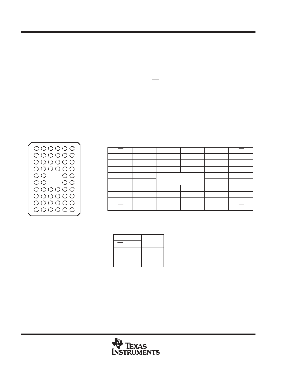
terminal assignments
1
2
3
4
5
6
A
1OE
NC
NC
NC
NC
2OE
B
1Y2
1Y1
GND
GND
1A1
1A2
C
1Y4
1Y3
VCC
VCC
1A3
1A4
D
2Y2
2Y1
GND
GND
2A1
2A2
E
2Y4
2Y3
2A3
2A4
F
3Y1
3Y2
3A2
3A1
G
3Y3
3Y4
GND
GND
3A4
3A3
H
4Y1
4Y2
VCC
VCC
4A2
4A1
J
4Y3
4Y4
GND
GND
4A4
4A3
K
4OE
NC
NC
NC
NC
3OE
NC - No internal connection
FUNCTION TABLE
(each 4-bit buffer)
INPUTS
OUTPUT
OE
A
OUTPUT
Y
L
H
H
L
L
L
H
X
Z
GQL OR ZQL PACKAGE
(TOP VIEW)
J
H
G
F
E
D
C
B
A
2
1
3
4
6
5
K
SN54LVTH162244, SN74LVTH162244
3.3 V ABT 16 BIT BUFFERS/DRIVERS
WITH 3 STATE OUTPUTS
SCBS258M - JUNE 1993 - REVISED SEPTEMBER 2003
3
POST OFFICE BOX 655303
·
DALLAS, TEXAS 75265
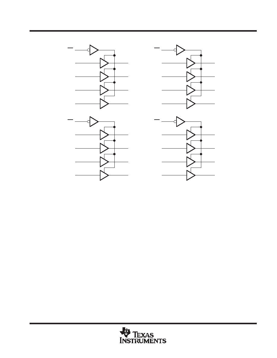
logic diagram (positive logic)
1OE
1A1
1A2
1A3
1A4
1Y1
1Y2
1Y3
1Y4
1
47
46
44
43
2
3
5
6
2OE
2A1
2A2
2A3
2A4
2Y1
2Y2
2Y3
2Y4
48
41
40
38
37
8
9
11
12
3OE
3A1
3A2
3A3
3A4
3Y1
3Y2
3Y3
3Y4
25
36
35
33
32
13
14
16
17
4OE
4A1
4A2
4A3
4A4
4Y1
4Y2
4Y3
4Y4
24
30
29
27
26
19
20
22
23
Pin numbers shown are for the DGG, DL, and WD packages.
absolute maximum ratings over operating free-air temperature range (unless otherwise noted)
Supply voltage range, V
CC
-0.5 V to 4.6 V
. . . . . . . . . . . . . . . . . . . . . . . . . . . . . . . . . . . . . . . . . . . . . . . . . . . . . . . . .
Input voltage range, V
I
(see Note 1)
-0.5 V to 7 V
. . . . . . . . . . . . . . . . . . . . . . . . . . . . . . . . . . . . . . . . . . . . . . . . . .
Voltage range applied to any output in the high-impedance
or power-off state, V
O
(see Note 1)
-0.5 V to 7 V
. . . . . . . . . . . . . . . . . . . . . . . . . . . . . . . . . . . . . . . . . . . . . . . .
Voltage range applied to any output in the high state, V
O
(see Note 1)
-0.5 V to V
CC
+ 0.5 V
. . . . . . . . . . . . .
Current into any output in the low state, I
O
30
mA
. . . . . . . . . . . . . . . . . . . . . . . . . . . . . . . . . . . . . . . . . . . . . . . . . .
Current into any output in the high state, I
O
(see Note 2)
30 mA
. . . . . . . . . . . . . . . . . . . . . . . . . . . . . . . . . . . . . .
Input clamp current, I
IK
(V
I
< 0)
-50 mA
. . . . . . . . . . . . . . . . . . . . . . . . . . . . . . . . . . . . . . . . . . . . . . . . . . . . . . . . . . .
Output clamp current, I
OK
(V
O
< 0)
-50 mA
. . . . . . . . . . . . . . . . . . . . . . . . . . . . . . . . . . . . . . . . . . . . . . . . . . . . . . . .
Package thermal impedance,
JA
(see Note 3): DGG package
70
°
C/W
. . . . . . . . . . . . . . . . . . . . . . . . . . . . . . .
DL package
63
°
C/W
. . . . . . . . . . . . . . . . . . . . . . . . . . . . . . . . .
GQL/ZQL package
42
°
C/W
. . . . . . . . . . . . . . . . . . . . . . . . . . .
Storage temperature range, T
stg
-65
°
C to 150
°
C
. . . . . . . . . . . . . . . . . . . . . . . . . . . . . . . . . . . . . . . . . . . . . . . . . . .
Stresses beyond those listed under "absolute maximum ratings" may cause permanent damage to the device. These are stress ratings only, and
functional operation of the device at these or any other conditions beyond those indicated under "recommended operating conditions" is not
implied. Exposure to absolute-maximum-rated conditions for extended periods may affect device reliability.
NOTES:
1. The input and output negative-voltage ratings may be exceeded if the input and output clamp-current ratings are observed.
2. This current flows only when the output is in the high state and VO > VCC.
3. The package thermal impedance is calculated in accordance with JESD 51-7.
SN54LVTH162244, SN74LVTH162244
3.3 V ABT 16 BIT BUFFERS/DRIVERS
WITH 3 STATE OUTPUTS
SCBS258M - JUNE 1993 - REVISED SEPTEMBER 2003
4
POST OFFICE BOX 655303
·
DALLAS, TEXAS 75265
recommended operating conditions (see Note 4)
SN54LVTH162244
SN74LVTH162244
UNIT
MIN
MAX
MIN
MAX
UNIT
VCC
Supply voltage
2.7
3.6
2.7
3.6
V
VIH
High-level input voltage
2
2
V
VIL
Low-level input voltage
0.8
0.8
V
VI
Input voltage
5.5
5.5
V
IOH
High-level output current
-12
-12
mA
IOL
Low-level output current
12
12
mA
t/
v
Input transition rise or fall rate
Outputs enabled
10
10
ns/V
t/
VCC
Power-up ramp rate
200
200
µ
s/V
TA
Operating free-air temperature
-55
125
-40
85
°
C
NOTE 4: All unused control inputs of the device must be held at VCC or GND to ensure proper device operation. Refer to the TI application report,
Implications of Slow or Floating CMOS Inputs, literature number SCBA004.
electrical characteristics over recommended operating free-air temperature range (unless
otherwise noted)
PARAMETER
TEST CONDITIONS
SN54LVTH162244
SN74LVTH162244
UNIT
PARAMETER
TEST CONDITIONS
MIN
TYP
MAX
MIN
TYP
MAX
UNIT
VIK
VCC = 2.7 V,
II = -18 mA
-1.2
-1.2
V
VOH
VCC = 3 V,
IOH = -12 mA
2
2
V
VOL
VCC = 3 V,
IOL = 12 mA
0.8
0.8
V
VCC = 0 or 3.6 V,
VI = 5.5 V
10
10
II
Control inputs
VCC = 3.6 V,
VI = VCC or GND
±
1
±
1
A
II
Data inputs
VCC = 3.6 V
VI = VCC
1
1
µ
A
Data inputs
VCC = 3.6 V
VI = 0
-5
-5
Ioff
VCC = 0,
VI or VO = 0 to 4.5 V
±
100
µ
A
VCC = 3 V
VI = 0.8 V
75
75
II(hold) Data inputs
VCC = 3 V
VI = 2 V
-75
-75
µ
A
II(hold) Data inputs
VCC = 3.6 V,
VI = 0 to 3.6 V
500
-750
µ
A
IOZH
VCC = 3.6 V,
VO = 3 V
5
5
µ
A
IOZL
VCC = 3.6 V,
VO = 0.5 V
-5
-5
µ
A
IOZPU
VCC = 0 to 1.5 V, VO = 0.5 V to 3 V,
OE = don't care
±
100*
±
100
µ
A
IOZPD
VCC = 1.5 V to 0, VO = 0.5 V to 3 V,
OE = don't care
±
100*
±
100
µ
A
VCC = 3.6 V,
Outputs high
0.19
0.19
ICC
VCC = 3.6 V,
IO = 0,
V = V
or GND
Outputs low
5
5
mA
ICC
IO = 0,
VI = VCC or GND
Outputs disabled
0.19
0.19
mA
ICC§
VCC = 3 V to 3.6 V, One input at VCC - 0.6 V,
Other inputs at VCC or GND
0.2
0.2
mA
Ci
VI = 3 V or 0
4
4
pF
Co
VO = 3 V or 0
9
9
pF
* On products compliant to MIL-PRF-38535, this parameter is not production tested.
All typical values are at VCC = 3.3 V, TA = 25
°
C.
This is the bus-hold maximum dynamic current. It is the minimum overdrive current required to switch the input from one state to another.
§ This is the increase in supply current for each input that is at the specified TTL voltage level, rather than VCC or GND.
SN54LVTH162244, SN74LVTH162244
3.3 V ABT 16 BIT BUFFERS/DRIVERS
WITH 3 STATE OUTPUTS
SCBS258M - JUNE 1993 - REVISED SEPTEMBER 2003
5
POST OFFICE BOX 655303
·
DALLAS, TEXAS 75265
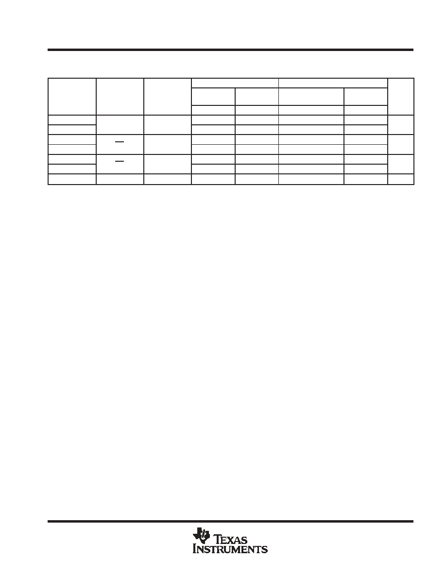
switching characteristics over recommended operating free-air temperature range, C
L
= 50 pF
(unless otherwise noted) (see Figure 1)
SN54LVTH162244
SN74LVTH162244
PARAMETER
FROM
(INPUT)
TO
(OUTPUT)
VCC = 3.3 V
±
0.3 V
VCC = 2.7 V
VCC = 3.3 V
±
0.3 V
VCC = 2.7 V
UNIT
(INPUT)
(OUTPUT)
MIN
MAX
MIN
MAX
MIN
TYP
MAX
MIN
MAX
tPLH
A
Y
1.1
4.6
5.1
1.4
3.4
4
4.8
ns
tPHL
A
Y
1.1
3.9
4.5
1.2
2.9
3.6
4.1
ns
tPZH
OE
Y
1.1
5.4
6.7
1.2
3.9
5.1
6.5
ns
tPZL
OE
Y
1.3
4.9
6.1
1.4
3.8
4.5
5.8
ns
tPHZ
OE
Y
1.6
5.9
6.5
2.2
4.4
5
5.4
ns
tPLZ
OE
Y
1
5.9
5.8
2
4.2
5
5.4
ns
tsk(o)
0.5
ns
All typical values are at VCC = 3.3 V, TA = 25
°
C.