www.ti.com
FEATURES
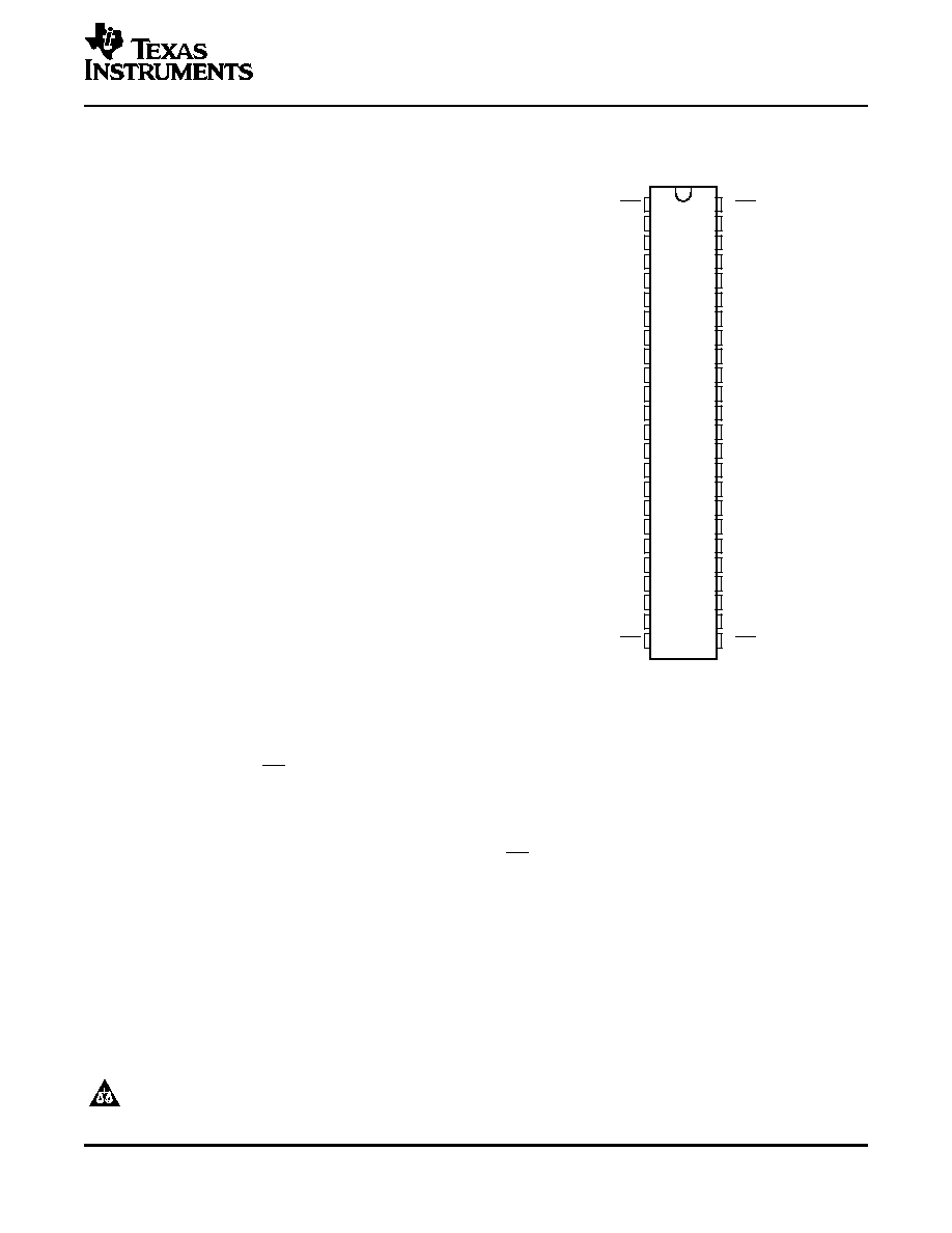
SN54LVTH16244A . . . WD PACKAGE
SN74LVTH16244A . . . DGG, DGV, OR DL PACKAGE
(TOP VIEW)
1
2
3
4
5
6
7
8
9
10
11
12
13
14
15
16
17
18
19
20
21
22
23
24
48
47
46
45
44
43
42
41
40
39
38
37
36
35
34
33
32
31
30
29
28
27
26
25
1OE
1Y1
1Y2
GND
1Y3
1Y4
V
CC
2Y1
2Y2
GND
2Y3
2Y4
3Y1
3Y2
GND
3Y3
3Y4
V
CC
4Y1
4Y2
GND
4Y3
4Y4
4OE
2OE
1A1
1A2
GND
1A3
1A4
V
CC
2A1
2A2
GND
2A3
2A4
3A1
3A2
GND
3A3
3A4
V
CC
4A1
4A2
GND
4A3
4A4
3OE
DESCRIPTION/ORDERING INFORMATION
SN54LVTH16244A, SN74LVTH16244A
3.3-V ABT 16-BIT BUFFERS/DRIVERS
WITH 3-STATE OUTPUTS
SCBS142Q ≠ MAY 1992 ≠ REVISED OCTOBER 2005
∑
Members of the Texas Instruments
Widebus TM Family
∑
State-of-the-Art Advanced BiCMOS
Technology (ABT) Design for 3.3-V
Operation and Low Static-Power
Dissipation
∑
Support Mixed-Mode Signal Operation
(5-V Input and Output Voltages With
3.3-V V
CC
)
∑
Support Unregulated Battery Operation
Down to 2.7 V
∑
Typical V
OLP
(Output Ground Bounce)
<0.8 V at V
CC
= 3.3 V, T
A
= 25
∞
C
∑
I
off
and Power-Up 3-State Support Hot
Insertion
∑
Bus Hold on Data Inputs Eliminates the Need
for External Pullup/Pulldown Resistors
∑
Latch-Up Performance Exceeds 500 mA
Per JESD 17
∑
ESD Protection Exceeds JESD 22
≠ 2000-V Human-Body Model (A114-A)
≠ 200-V Machine Model (A115-A)
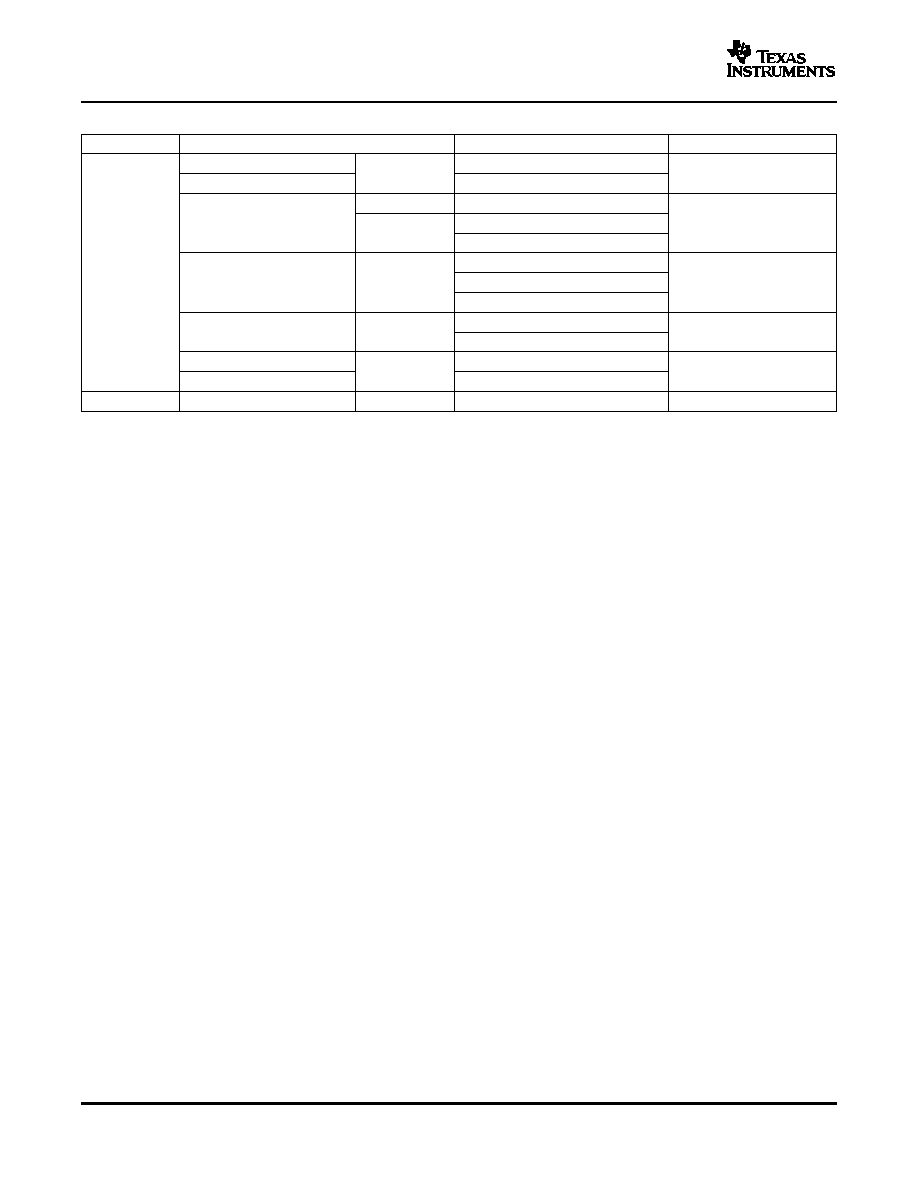
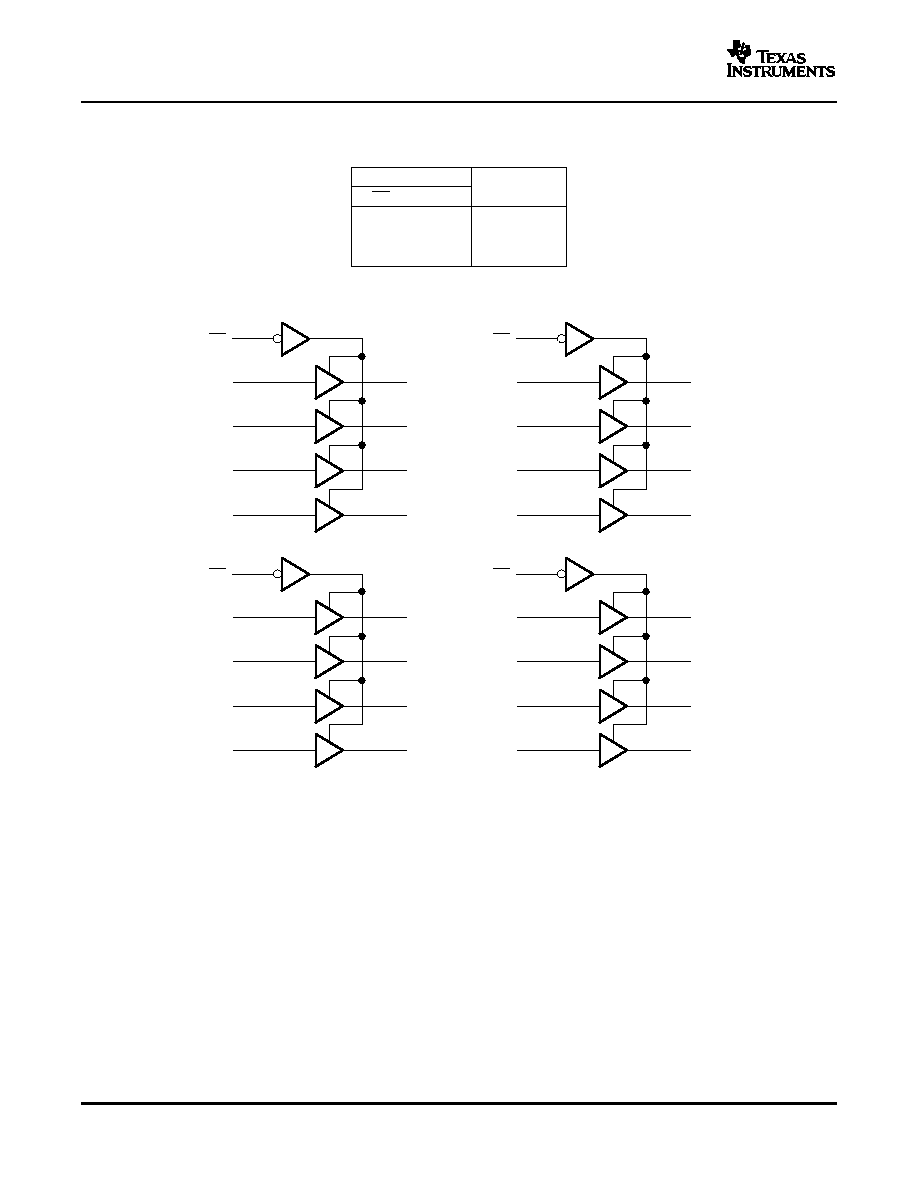
The 'LVTH16244A devices are 16-bit buffers and line drivers designed for low-voltage (3.3-V) V
CC
operation, but
with the capability to provide a TTL interface to a 5-V system environment. These devices can be used as four
4-bit buffers, two 8-bit buffers, or one 16-bit buffer. These devices provide true outputs and symmetrical
active-low output-enable (OE) inputs.
Active bus-hold circuitry holds unused or undriven inputs at a valid logic state. Use of pullup or pulldown resistors
with the bus-hold circuitry is not recommended.
When V
CC
is between 0 and 1.5 V, the devices are in the high-impedance state during power up or power down.
However, to ensure the high-impedance state above 1.5 V, OE should be tied to V
CC
through a pullup resistor;
the minimum value of the resistor is determined by the current-sinking capability of the driver.
These devices are fully specified for hot-insertion applications using I
off
and power-up 3-state. The I
off
circuitry
disables the outputs, preventing damaging current backflow through the devices when they are powered down.
The power-up 3-state circuitry places the outputs in the high-impedance state during power up and power down,
which prevents driver conflict.
Please be aware that an important notice concerning availability, standard warranty, and use in critical applications of Texas
Instruments semiconductor products and disclaimers thereto appears at the end of this data sheet.
Widebus is a trademark of Texas Instruments.
PRODUCTION DATA information is current as of publication date.
Copyright © 1992≠2005, Texas Instruments Incorporated
Products conform to specifications per the terms of the Texas
Instruments standard warranty. Production processing does not
necessarily include testing of all parameters.
www.ti.com
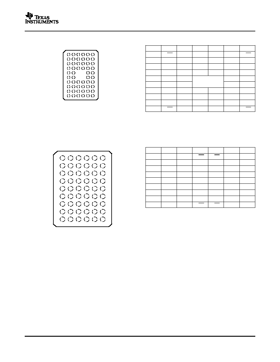
GQL OR ZQL PACKAGE
(TOP VIEW)
J
H
G
F
E
D
C
B
A
2
1
3 4
6
5
K
GRD OR ZRD PACKAGE
(TOP VIEW)
J
H
G
F
E
D
C
B
A
2
1
3
4
6
5
SN54LVTH16244A, SN74LVTH16244A
3.3-V ABT 16-BIT BUFFERS/DRIVERS
WITH 3-STATE OUTPUTS
SCBS142Q ≠ MAY 1992 ≠ REVISED OCTOBER 2005
TERMINAL ASSIGNMENTS
(1)
(56-Ball GQL/ZQL Package)
1
2
3
4
5
6
A
1OE
NC
NC
NC
NC
2OE
B
1Y2
1Y1
GND
GND
1A1
1A2
C
1Y4
1Y3
V
CC
V
CC
1A3
1A4
D
2Y2
2Y1
GND
GND
2A1
2A2
E
2Y4
2Y3
2A3
2A4
F
3Y1
3Y2
3A2
3A1
G
3Y3
3Y4
GND
GND
3A4
3A3
H
4Y1
4Y2
V
CC
V
CC
4A2
4A1
J
4Y3
4Y4
GND
GND
4A4
4A3
blk
K
4OE
NC
NC
NC
NC
3OE
blk
blk
(1)
NC ≠ No internal connection
xxxxx
xxxxx
xxxxx
TERMINAL ASSIGNMENTS
(1)
(54-Ball GRD/ZRD Package)
1
2
3
4
5
6
A
1Y1
NC
1OE
2OE
NC
1A1
B
1Y3
1Y2
NC
NC
1A2
1A3
C
2Y1
1Y4
V
CC
V
CC
1A4
2A1
D
2Y3
2Y2
GND
GND
2A2
2A3
E
3Y1
2Y4
GND
GND
2A4
3A1
F
3Y3
3Y2
GND
GND
3A2
3A3
G
4Y1
3Y4
V
CC
V
CC
3A4
4A1
H
4Y3
4Y2
NC
NC
4A2
4A3
J
4Y4
NC
4OE
3OE
NC
4A4
(1)
NC ≠ No internal connection
3
www.ti.com
Absolute Maximum Ratings
(1)
Recommended Operating Conditions
(1)
SN54LVTH16244A, SN74LVTH16244A
3.3-V ABT 16-BIT BUFFERS/DRIVERS
WITH 3-STATE OUTPUTS
SCBS142Q ≠ MAY 1992 ≠ REVISED OCTOBER 2005
over operating free-air temperature range (unless otherwise noted)
MIN
MAX
UNIT
V
CC
Supply voltage range
≠0.5
4.6
V
V
I
Input voltage range
(2)
≠0.5
7
V
V
O
Voltage range applied to any output in the high-impedance or power-off state
(2)
≠0.5
7
V
V
O
Voltage range applied to any output in the high state
(2)
≠0.5 V
CC
+ 0.5
SN54LVTH16244A
96
I
O
Current into any output in the low state
V
SN74LVTH16244A
128
SN54LVTH16244A
48
I
O
Current into any output in the high state
(3)
V
SN74LVTH16244A
64
I
IK
Input clamp current
V
I
< 0
≠50
mA
I
OK
Output clamp current
V
O
< 0
≠50
mA
DGG package
70
DGV package
58
JA
Package thermal impedance
(4)
DL package
63
∞
C/W
GQL/ZQL package
42
GRD/ZRD package
36
T
stg
Storage temperature range
≠65
150
∞
C
(1)
Stresses beyond those listed under "absolute maximum ratings" may cause permanent damage to the device. These are stress ratings
only, and functional operation of the device at these or any other conditions beyond those indicated under "recommended operating
conditions" is not implied. Exposure to absolute-maximum-rated conditions for extended periods may affect device reliability.
(2)
The input and output negative-voltage ratings may be exceeded if the input and output clamp-current ratings are observed.
(3)
The current flows only when the output is in the high state and V
O
> V
CC
.
(4)
The package thermal impedance is calculated in accordance with JESD 51-7.
SN54LVTH16244A
SN74LVTH16244A
UNIT
MIN
MAX
MIN
MAX
V
CC
Supply voltage
2.7
3.8
2.7
3.8
V
V
IH
High-level input voltage
2
2
V
V
IL
Low-level input voltage
0.8
0.8
V
V
I
Input voltage
5.5
5.5
V
I
OH
High-level output current
≠25
≠32
mA
I
OL
Low-level output current
48
64
mA
t/
v
Input transition rise or fall rate
Outputs enabled
10
10
ns/V
t/
V
CC
Power-up ramp rate
200
200
µ
s/V
T
A
Operating free-air temperature
≠55
125
≠40
85
∞
C
(1)
All unused inputs of the device must be held at V
CC
or GND to ensure proper device operation. Refer to the TI application report,
Implications of Slow or Floating CMOS Inputs, literature number SCBA004.
5