www.ti.com
FEATURES
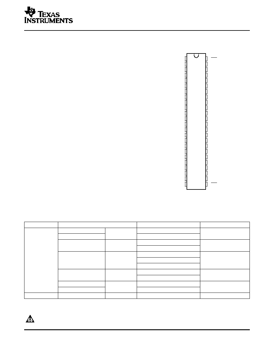
SN54LVTH16245A . . . WD PACKAGE
SN74LVTH16245A . . . DGG, DGV, OR DL PACKAGE
(TOP VIEW)
1
2
3
4
5
6
7
8
9
10
11
12
13
14
15
16
17
18
19
20
21
22
23
24
48
47
46
45
44
43
42
41
40
39
38
37
36
35
34
33
32
31
30
29
28
27
26
25
1DIR
1B1
1B2
GND
1B3
1B4
V
CC
1B5
1B6
GND
1B7
1B8
2B1
2B2
GND
2B3
2B4
V
CC
2B5
2B6
GND
2B7
2B8
2DIR
1OE
1A1
1A2
GND
1A3
1A4
V
CC
1A5
1A6
GND
1A7
1A8
2A1
2A2
GND
2A3
2A4
V
CC
2A5
2A6
GND
2A7
2A8
2OE
DESCRIPTION/ORDERING INFORMATION
SN54LVTH16245A, SN74LVTH16245A
3.3-V ABT 16-BIT BUS TRANSCEIVERS
WITH 3-STATE OUTPUTS
SCBS143Q ≠ MAY 1992 ≠ REVISED OCTOBER 2005
∑
Members of the Texas Instruments WidebusTM
Family
∑
State-of-the-Art Advanced BiCMOS
Technology (ABT) Design for 3.3-V Operation
and Low Static-Power Dissipation
∑
Support Mixed-Mode Signal Operation (5-V
Input and Output Voltages With 3.3-V V
CC
)
∑
Support Unregulated Battery Operation Down
to 2.7 V
∑
Typical V
OLP
(Output Ground Bounce) <0.8 V
at V
CC
= 3.3 V, T
A
= 25
∞
C
∑
Distributed V
CC
and GND Pins Minimize
High-Speed Switching Noise
∑
Flow-Through Architecture Optimizes PCB
Layout
∑
I
off
and Power-Up 3-State Support Hot
Insertion
∑
Bus Hold on Data Inputs Eliminates the Need
for External Pullup/Pulldown Resistors
∑
Latch-Up Performance Exceeds 500 mA Per
JESD 17
∑
ESD Protection Exceeds JESD 22
≠ 2000-V Human-Body Model (A114-A)
≠ 200-V Machine Model (A115-A)
ORDERING INFORMATION
T
A
PACKAGE
(1)
ORDERABLE PART NUMBER
TOP-SIDE MARKING
FBGA ≠ GRD
SN74LVTH16245AGRDR
Tape and reel
LL245A
FBGA ≠ ZRD (Pb-free)
SN74LVTH16245AZRDR
74LVTH16245ADLG4
SSOP ≠ DL
Tape and reel
LVTH16245A
74LVTH16245ADLRG4
SN74LVTH16245ADGGR
≠40
∞
C to 85
∞
C
TSSOP ≠ DGG
Tape and reel
74LVTH16245ADGGRE4
LVTH16245A
74LVTH16245ADGGRG4
SN74LVTH16245ADGVR
TVSOP ≠ DGV
Tape and reel
LL245A
74LVTH16245ADGVRE4
VFBGA ≠ GQL
SN74LVTH16245AKR
Tape and reel
LL245A
VFBGA ≠ ZQL (Pb-free)
74LVTH16245AZQLR
≠55
∞
C to 125
∞
C
CFP ≠ WD
Tube
SNJ54LVTH16245AWD
SNJ54LVTH16245AWD
(1)
Package drawings, standard packing quantities, thermal data, symbolization, and PCB design guidelines are available at
www.ti.com/sc/package.
Please be aware that an important notice concerning availability, standard warranty, and use in critical applications of Texas
Instruments semiconductor products and disclaimers thereto appears at the end of this data sheet.
Widebus is a trademark of Texas Instruments.
PRODUCTION DATA information is current as of publication date.
Copyright © 1992≠2005, Texas Instruments Incorporated
Products conform to specifications per the terms of the Texas
On products compliant to MIL-PRF-38535, all parameters are
Instruments standard warranty. Production processing does not
tested unless otherwise noted. On all other products, production
necessarily include testing of all parameters.
processing does not necessarily include testing of all parameters.
www.ti.com
DESCRIPTION/ORDERING INFORMATION (CONTINUED)
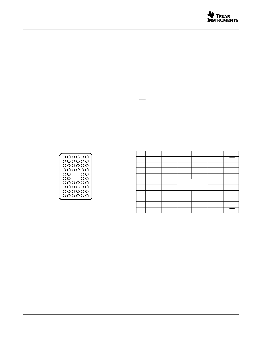
GQL OR ZQL PACKAGE
(TOP VIEW)
J
H
G
F
E
D
C
B
A
2
1
3 4
6
5
K
abc
SN54LVTH16245A, SN74LVTH16245A
3.3-V ABT 16-BIT BUS TRANSCEIVERS
WITH 3-STATE OUTPUTS
SCBS143Q ≠ MAY 1992 ≠ REVISED OCTOBER 2005
The 'LVTH16245A devices are 16-bit (dual-octal) noninverting 3-state transceivers designed for low-voltage
(3.3-V) V
CC
operation, but with the capability to provide a TTL interface to a 5-V system environment.
The devices are designed for asynchronous communication between two data buses. The logic levels of the
direction-control (DIR) input and the output-enable (OE) input activate either the B-port outputs or the A-port
outputs or place both output ports into the high-impedance mode. The device transmits data from the A bus to
the B bus when the B-port outputs are activated, and from the B bus to the A bus when the A-port outputs are
activated. The input circuitry on both A and B ports is always active and must have a logic HIGH or LOW level
applied to prevent excess I
CC
and I
CCZ
.
Active bus-hold circuitry holds unused or undriven inputs at a valid logic state. Use of pullup or pulldown resistors
with the bus-hold circuitry is not recommended.
When V
CC
is between 0 and 1.5 V, the devices are in the high-impedance state during power up or power down.
However, to ensure the high-impedance state above 1.5 V, OE should be tied to V
CC
through a pullup resistor;
the minimum value of the resistor is determined by the current-sinking capability of the driver.
These devices are fully specified for hot-insertion applications using I
off
and power-up 3-state. The I
off
circuitry
disables the outputs, preventing damaging current backflow through the devices when they are powered down.
The power-up 3-state circuitry places the outputs in the high-impedance state during power up and power down,
which prevents driver conflict.
TERMINAL ASSIGNMENTS
(1)
(56-Ball GQL/ZQL Package)
1
2
3
4
5
6
A
1DIR
NC
NC
NC
NC
1OE
B
1B2
1B1
GND
GND
1A1
1A2
C
1B4
1B3
V
CC
V
CC
1A3
1A4
D
1B6
1B5
GND
GND
1A5
1A6
E
1B8
1B7
1A7
1A8
F
2B1
2B2
2A2
2A1
G
2B3
2B4
GND
GND
2A4
2A3
H
2B5
2B6
V
CC
V
CC
2A6
2A5
J
2B7
2B8
GND
GND
2A8
2A7
K
2DIR
NC
NC
NC
NC
2OE
abc
abc
(1)
NC ≠ No internal connection
2
www.ti.com
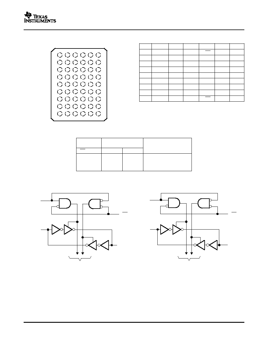
GRD OR ZRD PACKAGE
(TOP VIEW)
J
H
G
F
E
D
C
B
A
2
1
3
4
6
5
To Seven Other Channels
1DIR
1A1
1B1
1OE
To Seven Other Channels
2DIR
2A1
2B1
2OE
1
47
24
36
48
2
25
13
SN54LVTH16245A, SN74LVTH16245A
3.3-V ABT 16-BIT BUS TRANSCEIVERS
WITH 3-STATE OUTPUTS
SCBS143Q ≠ MAY 1992 ≠ REVISED OCTOBER 2005
TERMINAL ASSIGNMENTS
(1)
(54-Ball GRD/ZRD Package)
1
2
3
4
5
6
A
1B1
NC
1DIR
1OE
NC
1A1
B
1B3
1B2
NC
NC
1A2
1A3
C
1B5
1B4
V
CC
V
CC
1A4
1A5
D
1B7
1B6
GND
GND
1A6
1A7
E
2B1
1B8
GND
GND
1A8
2A1
F
2B3
2B2
GND
GND
2A2
2A3
G
2B5
2B4
V
CC
V
CC
2A4
2A5
H
2B7
2B6
NC
NC
2A6
2A7
J
2B8
NC
2DIR
2OE
NC
2A8
(1)
NC ≠ No internal connection
FUNCTION TABLE
(1)
(EACH 8-BIT SECTION)
CONTROL
OUTPUT CIRCUITS
INPUTS
OPERATION
OE
DIR
A PORT
B PORT
L
L
Enabled
Hi-Z
B data to A bus
L
H
Hi-Z
Enabled
A data to B bus
H
X
Hi-Z
Hi-Z
Isolation
(1)
Input circuits of the data I/Os always are active.
LOGIC DIAGRAM (POSITIVE LOGIC)
3
www.ti.com
Absolute Maximum Ratings
(1)
Recommended Operating Conditions
(1)
SN54LVTH16245A, SN74LVTH16245A
3.3-V ABT 16-BIT BUS TRANSCEIVERS
WITH 3-STATE OUTPUTS
SCBS143Q ≠ MAY 1992 ≠ REVISED OCTOBER 2005
over operating free-air temperature range (unless otherwise noted)
MIN
MAX
UNIT
V
CC
Supply voltage range
≠0.5
4.6
V
V
I
Input voltage range
(2)
≠0.5
7
V
V
O
Voltage range applied to any output in the high-impedance or power-off state
(2)
≠0.5
7
V
V
O
Voltage range applied to any output in the high state
(2)
≠0.5
V
CC
+ 0.5
V
SN54LVTH16245A
96
I
O
Current into any output in the low state
mA
SN74LVTH16245A
128
SN54LVTH16245A
48
I
O
Current into any output in the high state
(3)
mA
SN74LVTH16245A
64
I
IK
Input clamp current
V
I
< 0
≠50
mA
I
OK
Output clamp current
V
O
< 0
≠50
mA
DGG package
70
DGV package
58
JA
Package thermal impedance
(4)
DL package
63
∞
C/W
GQL/ZQL package
42
GRD/ZRD package
36
T
stg
Storage temperature range
≠65
150
∞
C
(1)
Stresses beyond those listed under "absolute maximum ratings" may cause permanent damage to the device. These are stress ratings
only, and functional operation of the device at these or any other conditions beyond those indicated under "recommended operating
conditions" is not implied. Exposure to absolute-maximum-rated conditions for extended periods may affect device reliability.
(2)
The input and output negative-voltage ratings may be exceeded if the input and output clamp-current ratings are observed.
(3)
This current flows only when the output is in the high state and V
O
> V
CC
.
(4)
The package thermal impedance is calculated in accordance with JESD 51-7.
SN54LVTH16245A
SN74LVTH16245A
UNIT
MIN
MAX
MIN
MAX
V
CC
Supply voltage
2.7
3.6
2.7
3.6
V
V
IH
High-level input voltage
2
2
V
V
IL
Low-level input voltage
0.8
0.8
V
V
I
Input voltage
5.5
5.5
V
I
OH
High-level output current
≠24
≠32
mA
I
OL
Low-level output current
48
64
mA
t/
v
Input transition rise or fall rate
Outputs enabled
10
10
ns/V
t/
V
CC
Power-up ramp rate
200
200
µ
s/V
T
A
Operating free-air temperature
≠55
125
≠40
85
∞
C
(1)
All unused control inputs of the device must be held at V
CC
or GND to ensure proper device operation. Refer to the TI application report,
Implications of Slow or Floating CMOS Inputs, literature number SCBA004.
4
www.ti.com
Electrical Characteristics
SN54LVTH16245A, SN74LVTH16245A
3.3-V ABT 16-BIT BUS TRANSCEIVERS
WITH 3-STATE OUTPUTS
SCBS143Q ≠ MAY 1992 ≠ REVISED OCTOBER 2005
over recommended operating free-air temperature range (unless otherwise noted)
SN54LVTH16245A
SN74LVTH16245A
PARAMETER
TEST CONDITIONS
UNIT
MIN
TYP
(1)
MAX
MIN TYP
(1)
MAX
V
IK
V
CC
= 2.7 V,
I
I
= ≠18 mA
≠1.2
≠1.2
V
V
CC
= 2.7 V to 3.6 V,
I
OH
= ≠100
µ
A
V
CC
≠ 0.2
V
CC
≠ 0.2
V
CC
= 2.7 V,
I
OH
= ≠8 mA
2.4
2.4
V
OH
V
I
OH
= ≠24 mA
2
V
CC
= 3 V
I
OH
= ≠32 mA
2
I
OL
= 100
µ
A
0.2
0.2
V
CC
= 2.7 V
I
OL
= 24 mA
0.5
0.5
I
OL
= 16 mA
0.4
0.4
V
OL
V
I
OL
= 32 mA
0.5
0.5
V
CC
= 3 V
I
OL
= 48 mA
0.55
I
OL
= 64 mA
0.55
V
CC
= 3.6 V,
V
I
= V
CC
or GND
±
1
±
1
Control
inputs
V
CC
= 0 or 3.6 V,
V
I
= 5.5 V
10
10
I
I
V
I
= 5.5 V
20
20
µ
A
A or B
V
CC
= 3.6 V
V
I
= V
CC
5
5
port
(2)
V
I
= 0
≠5
≠5
I
off
V
CC
= 0,
V
I
or V
O
= 0 to 4.5 V
±
100
µ
A
V
I
= 0.8 V
75
75
V
CC
= 3 V
A or B
V
I
= 2 V
≠75
≠75
I
I(hold)
µ
A
port
500
V
CC
= 3.6 V,
(3)
V
I
= 0 to 3.6 V
≠750
V
CC
= 0 to 1.5 V, V
O
= 0.5 V to 3 V,
I
OZPU
±
100
(4)
±
100
µ
A
OE = don't care
V
CC
= 1.5 V to 0, V
O
= 0.5 V to 3 V,
I
OZPD
±
100
(4)
±
100
µ
A
OE = don't care
Outputs high
0.19
0.19
V
CC
= 3.6 V,
I
CC
I
O
= 0,
Outputs low
5
5
mA
V
I
= V
CC
or GND
Outputs disabled
0.19
0.19
V
CC
= 3 V to 3.6 V, One input at V
CC
≠ 0.6 V,
I
CC
(5)
0.2
0.2
mA
Other inputs at V
CC
or GND
C
i
V
I
= 3 V or 0
4
4
pF
C
io
V
O
= 3 V or 0
10
10
pF
(1)
All typical values are at V
CC
= 3.3 V, T
A
= 25
∞
C.
(2)
Unused pins at V
CC
or GND
(3)
This is the bus-hold maximum dynamic current. It is the minimum overdrive current required to switch the input from one state to
another.
(4)
On products compliant to MIL-PRF-38535, this parameter is not production tested.
(5)
This is the increase in supply current for each input that is at the specified TTL voltage level, rather than V
CC
or GND.
5