Äîêóìåíòàöèÿ è îïèñàíèÿ www.docs.chipfind.ru
www.ti.com
FEATURES
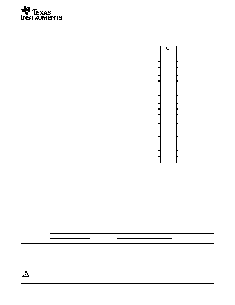
SN54LVTH16373 . . . WD PACKAGE
SN74LVTH16373 . . . DGG OR DL PACKAGE
(TOP VIEW)
1
2
3
4
5
6
7
8
9
10
11
12
13
14
15
16
17
18
19
20
21
22
23
24
48
47
46
45
44
43
42
41
40
39
38
37
36
35
34
33
32
31
30
29
28
27
26
25
1OE
1Q1
1Q2
GND
1Q3
1Q4
V
CC
1Q5
1Q6
GND
1Q7
1Q8
2Q1
2Q2
GND
2Q3
2Q4
V
CC
2Q5
2Q6
GND
2Q7
2Q8
2OE
1LE
1D1
1D2
GND
1D3
1D4
V
CC
1D5
1D6
GND
1D7
1D8
2D1
2D2
GND
2D3
2D4
V
CC
2D5
2D6
GND
2D7
2D8
2LE
DESCRIPTION/ORDERING INFORMATION
SN54LVTH16373, SN74LVTH16373
3.3-V ABT 16-BIT TRANSPARENT D-TYPE LATCHES
WITH 3-STATE OUTPUTS
SCBS144O MAY 1992 REVISED OCTOBER 2005
·
Members of the Texas Instruments WidebusTM
Family
·
State-of-the-Art Advanced BiCMOS
Technology (ABT) Design for 3.3-V Operation
and Low Static-Power Dissipation
·
Support Mixed-Mode Signal Operation (5-V
Input and Output Voltages With 3.3-V V
CC
)
·
Support Unregulated Battery Operation Down
to 2.7 V
·
Typical V
OLP
(Output Ground Bounce) <0.8 V
at V
CC
= 3.3 V, T
A
= 25
°
C
·
I
off
and Power-Up 3-State Support Hot
Insertion
·
Bus Hold on Data Inputs Eliminates the Need
for External Pullup/Pulldown Resistors
·
Distributed V
CC
and GND Pins Minimize
High-Speed Switching Noise
·
Flow-Through Architecture Optimizes PCB
Layout
·
Latch-Up Performance Exceeds 500 mA Per
JESD 17
·
ESD Protection Exceeds JESD 22
2000-V Human-Body Model (A114-A)
200-V Machine Model (A115-A)
The 'LVTH16373 devices are 16-bit transparent D-type latches with 3-state outputs designed for low-voltage
(3.3-V) V
CC
operation, but with the capability to provide a TTL interface to a 5-V system environment. These
devices are particularly suitable for implementing buffer registers, I/O ports, bidirectional bus drivers, and working
registers.
ORDERING INFORMATION
T
A
PACKAGE
(1)
ORDERABLE PART NUMBER
TOP-SIDE MARKING
FBGA GRD
SN74LVTH16373GRDR
Tape and reel
LL373
FBGA ZRD (Pb-free)
SN74LVTH16373ZRDR
Tube
SN74LVTH16373DL
SSOP DL
LVTH16373
40
°
C to 85
°
C
Tape and reel
SN74LVTH16373DLR
TSSOP DGG
Tape and reel
SN74LVTH16373DGGR
LVTH16373
VFBGA GQL
SN74LVTH16373GQLR
Tape and reel
LL373
VFBGA ZQL (Pb-free)
SN74LVTH16373ZQLR
55
°
C to 125
°
C
CFP WD
Tube
SNJ54LVTH16373WD
SNJ54LVTH16373WD
(1)
Package drawings, standard packing quantities, thermal data, symbolization, and PCB design guidelines are available at
www.ti.com/sc/package.
Please be aware that an important notice concerning availability, standard warranty, and use in critical applications of Texas
Instruments semiconductor products and disclaimers thereto appears at the end of this data sheet.
Widebus is a trademark of Texas Instruments.
PRODUCTION DATA information is current as of publication date.
Copyright © 19922005, Texas Instruments Incorporated
Products conform to specifications per the terms of the Texas
On products compliant to MIL-PRF-38535, all parameters are
Instruments standard warranty. Production processing does not
tested unless otherwise noted. On all other products, production
necessarily include testing of all parameters.
processing does not necessarily include testing of all parameters.
www.ti.com
DESCRIPTION/ORDERING INFORMATION (CONTINUED)
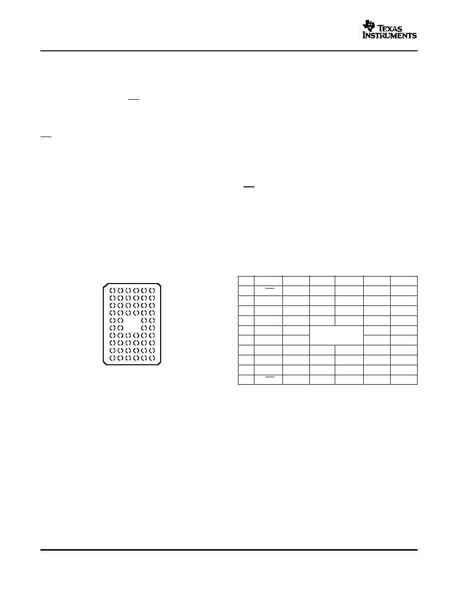
GQL OR ZQL PACKAGE
(TOP VIEW)
J
H
G
F
E
D
C
B
A
2
1
3 4
6
5
K
SN54LVTH16373, SN74LVTH16373
3.3-V ABT 16-BIT TRANSPARENT D-TYPE LATCHES
WITH 3-STATE OUTPUTS
SCBS144O MAY 1992 REVISED OCTOBER 2005
These devices can be used as two 8-bit latches or one 16-bit latch. When the latch-enable (LE) input is high, the
Q outputs follow the data (D) inputs. When LE is taken low, the Q outputs are latched at the levels set up at the
D inputs.
A buffered output-enable (OE) input can be used to place the eight outputs in either a normal logic state (high or
low logic levels) or a high-impedance state. In the high-impedance state, the outputs neither load nor drive the
bus lines significantly. The high-impedance state and the increased drive provide the capability to drive bus lines
without interface or pullup components.
OE does not affect internal operations of the latch. Old data can be retained or new data can be entered while
the outputs are in the high-impedance state.
Active bus-hold circuitry holds unused or undriven inputs at a valid logic state. Use of pullup or pulldown resistors
with the bus-hold circuitry is not recommended.
When V
CC
is between 0 and 1.5 V, the devices are in the high-impedance state during power up or power down.
However, to ensure the high-impedance state above 1.5 V, OE should be tied to V
CC
through a pullup resistor;
the minimum value of the resistor is determined by the current-sinking capability of the driver.
These devices are fully specified for hot-insertion applications using I
off
and power-up 3-state. The I
off
circuitry
disables the outputs, preventing damaging current backflow through the devices when they are powered down.
The power-up 3-state circuitry places the outputs in the high-impedance state during power up and power down,
which prevents driver conflict.
TERMINAL ASSIGNMENTS
(1)
(56-Ball GQL/ZQL Package)
1
2
3
4
5
6
A
1OE
NC
NC
NC
NC
1CLK
B
1Q2
1Q1
GND
GND
1D1
1D2
C
1Q4
1Q3
V
CC
V
CC
1D3
1D4
D
1Q6
1Q5
GND
GND
1D5
1D6
E
1Q8
1Q7
1D7
1D8
F
2Q1
2Q2
2D2
2D1
G
2Q3
2Q4
GND
GND
2D4
2D3
H
2Q5
2Q6
V
CC
V
CC
2D6
2D5
J
2Q7
2Q8
GND
GND
2D8
2D7
K
2OE
NC
NC
NC
NC
2CLK
(1)
NC No internal connection
2
www.ti.com
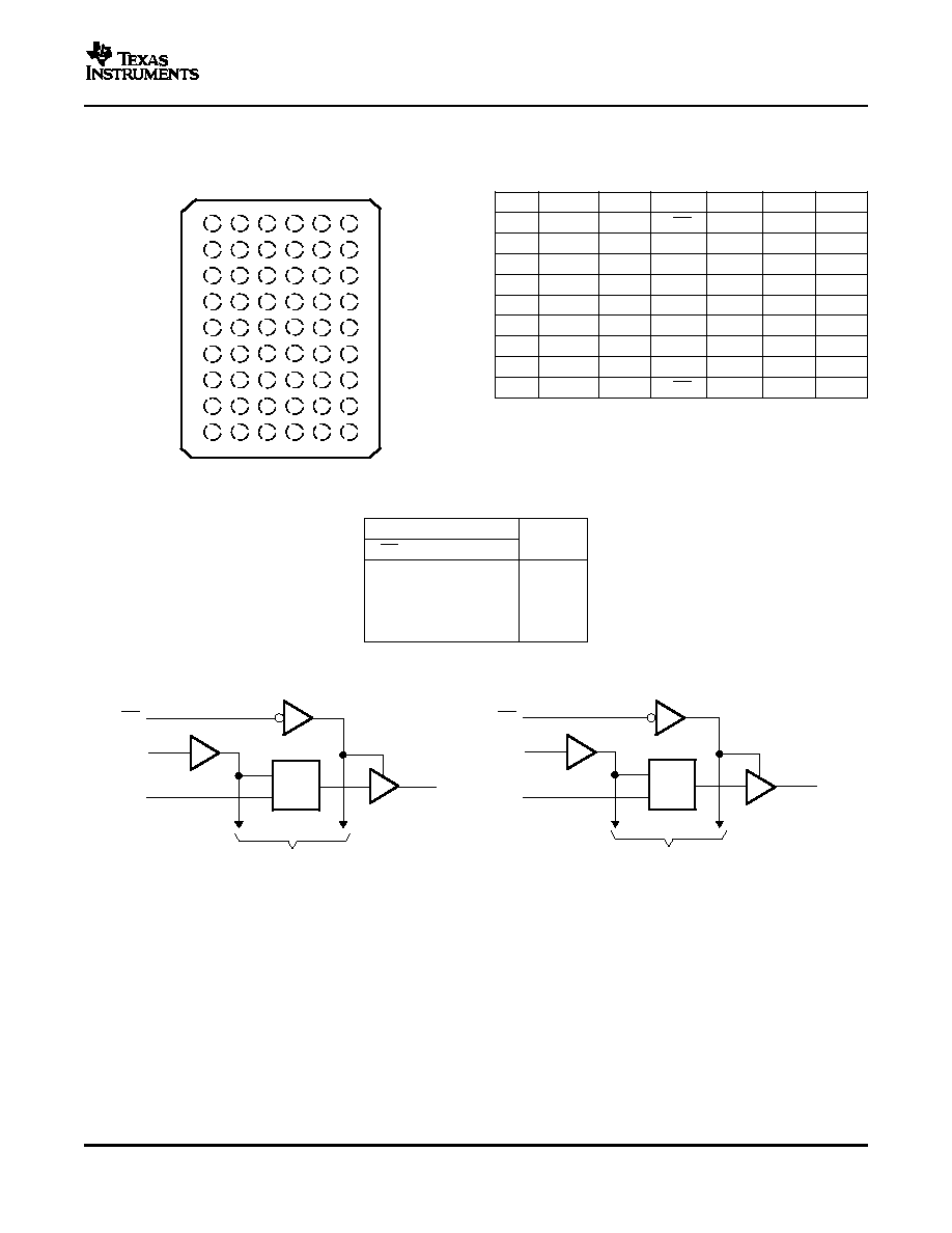
GRD OR ZRD PACKAGE
(TOP VIEW)
J
H
G
F
E
D
C
B
A
2
1
3
4
6
5
1OE
1LE
1D1
To Seven Other Channels
1Q1
2OE
2LE
2D1
2Q1
To Seven Other Channels
1
48
47
24
25
36
C1
1D
13
2
C1
1D
Pin numbers shown are for the DGG, DL, and WD packages.
SN54LVTH16373, SN74LVTH16373
3.3-V ABT 16-BIT TRANSPARENT D-TYPE LATCHES
WITH 3-STATE OUTPUTS
SCBS144O MAY 1992 REVISED OCTOBER 2005
TERMINAL ASSIGNMENTS
(1)
(54-Ball GRD/ZRD Package)
1
2
3
4
5
6
A
1Q1
NC
1OE
1LE
NC
1D1
B
1Q3
1Q2
NC
NC
1D2
1D3
C
1Q5
1Q4
V
CC
V
CC
1D4
1D5
D
1Q7
1Q6
GND
GND
1D6
1D7
E
2Q1
1Q8
GND
GND
1D8
2D1
F
2Q3
2Q2
GND
GND
2D2
2D3
G
2Q5
2Q4
V
CC
V
CC
2D4
2D5
H
2Q7
2Q6
NC
NC
2D6
2D7
J
2Q8
NC
2OE
2LE
NC
2D8
(1)
NC No internal connection
FUNCTION TABLE
(8-BIT SECTION)
INPUTS
OUTPUT
Q
OE
CLK
D
L
H
H
H
L
H
L
L
L
L
X
Q
0
H
X
X
Z
LOGIC DIAGRAM (POSITIVE LOGIC)
3
www.ti.com
Absolute Maximum Ratings
(1)
Recommended Operating Conditions
(1)
SN54LVTH16373, SN74LVTH16373
3.3-V ABT 16-BIT TRANSPARENT D-TYPE LATCHES
WITH 3-STATE OUTPUTS
SCBS144O MAY 1992 REVISED OCTOBER 2005
over operating free-air temperature range (unless otherwise noted)
MIN
MAX
UNIT
V
CC
Supply voltage range
0.5
4.6
V
V
I
Input voltage range
(2)
0.5
7
V
V
O
Voltage range applied to any output in the high-impedance or power-off state
(2)
0.5
7
V
V
O
Voltage range applied to any output in the high state
(2)
0.5
V
CC
+ 0.5
V
SN54LVTH16373
96
I
O
Current into any output in the low state
mA
SN74LVTH16373
128
SN54LVTH16373
48
I
O
Current into any output in the high state
(3)
mA
SN74LVTH16373
64
I
IK
Input clamp current
V
I
< 0
50
mA
I
OK
Output clamp current
V
O
< 0
50
mA
DGG package
70
DL package
63
JA
Package thermal impedance
(4)
°
C
GQL/ZQL package
42
GRD/ZRD package
36
T
stg
Storage temperature range
65
150
°
C
(1)
Stresses beyond those listed under "absolute maximum ratings" may cause permanent damage to the device. These are stress ratings
only, and functional operation of the device at these or any other conditions beyond those indicated under "recommended operating
conditions" is not implied. Exposure to absolute-maximum-rated conditions for extended periods may affect device reliability.
(2)
The input and output negative-voltage ratings may be exceeded if the input and output clamp-current ratings are observed.
(3)
This current flows only when the output is in the high state and V
O
> V
CC
.
(4)
The package thermal impedance is calculated in accordance with JESD 51-7.
SN54LVTH16373
SN74LVTH16373
UNIT
MIN
MAX
MIN
MAX
V
CC
Supply voltage
2.7
3.6
2.7
3.6
V
V
IH
High-level input voltage
2
2
V
V
IL
Low-level input voltage
0.8
0.8
V
V
I
Input voltage
5.5
5.5
V
I
OH
High-level output current
24
32
mA
I
OL
Low-level output current
48
64
mA
t/
v
Input transition rise or fall rate
Outpts enabled
10
10
ns/V
t/
V
CC
Power-up ramp rate
200
200
µ
s/V
T
A
Operating free-air temperature
55
125
40
85
°
C
(1)
All unused control inputs of the device must be held at V
CC
or GND to ensure proper device operation. Refer to the TI application report,
Implications of Slow or Floating CMOS Inputs, literature number SCBA004.
4
www.ti.com
Electrical Characteristics
SN54LVTH16373, SN74LVTH16373
3.3-V ABT 16-BIT TRANSPARENT D-TYPE LATCHES
WITH 3-STATE OUTPUTS
SCBS144O MAY 1992 REVISED OCTOBER 2005
over recommended operating free-air temperature range (unless otherwise noted)
SN54LVTH16373
SN74LVTH16373
PARAMETER
TEST CONDITIONS
UNIT
MIN TYP
(1)
MAX
MIN TYP
(1)
MAX
V
IK
V
CC
= 2.7 V,
I
I
= 18 mA
1.2
1.2
V
V
CC
= 2.7 V to 3.6 V,
I
OH
= 100
µ
A
V
CC
0.2
V
CC
0.2
V
CC
= 2.7 V,
I
OH
= 8 mA
2.4
2.4
V
OH
V
I
OH
= 24 mA
2
V
CC
= 3 V
I
OH
= 32 mA
2
I
OL
= 100
µ
A
0.2
0.2
V
CC
= 2.7 V
I
OL
= 24 mA
0.5
0.5
I
OL
= 16 mA
0.4
0.4
V
OL
V
I
OL
= 32 mA
0.5
0.5
V
CC
= 3 V
I
OL
= 48 mA
0.55
I
OL
= 64 mA
0.55
V
CC
= 0 or 3.6 V,
V
I
= 5.5 V
10
10
Control
V
CC
= 3.6 V,
V
I
= V
CC
or GND
±
1
±
1
inputs
I
I
µ
A
V
I
= V
CC
1
1
Data
V
CC
= 3.6 V
inputs
V
I
= 0
5
5
I
off
V
CC
= 0,
V
I
or V
O
= 0 to 4.5 V
±
100
µ
A
V
I
= 0.8 V
75
75
V
CC
= 3 V
Data
I
I(hold)
V
I
= 2 V
75
75
µ
A
inputs
V
CC
= 3.6 V,
(2)
V
I
= 0 to 3.6 V
±
500
I
OZH
V
CC
= 3.6 V,
V
O
= 3 V
5
5
µ
A
I
OZL
V
CC
= 3.6 V,
V
O
= 0.5 V
5
5
µ
A
V
CC
= 0 to 1.5 V, V
O
= 0.5 V to 3 V,
I
OZPU
±
100
(3)
±
100
µ
A
OE = don't care
V
CC
= 1.5 V to 0, V
O
= 0.5 V to 3 V,
I
OZPD
±
100
(3)
±
100
µ
A
OE = don't care
Outputs high
0.19
0.19
V
CC
= 3.6 V,
I
CC
I
O
= 0,
Outputs low
5
5
mA
V
I
= V
CC
or GND
Outputs disabled
0.19
0.19
V
CC
= 3 V to 3.6 V, One input at V
CC
0.6 V,
I
CC
(4)
0.2
0.2
mA
Other inputs at V
CC
or GND
C
i
V
I
= 3 V or 0
3
3
pF
C
o
V
O
= 3 V or 0
9
9
pF
(1)
All typical values are at V
CC
= 3.3 V, T
A
= 25
°
C.
(2)
This is the bus-hold maximum dynamic current. It is the minimum overdrive current required to switch the input from one state to
another.
(3)
On products compliant to MIL-PRF-38535, this parameter is not production tested.
(4)
This is the increase in supply current for each input that is at the specified TTL voltage level, rather than V
CC
or GND.
5
Document Outline