 | –≠–ª–µ–∫—Ç—Ä–æ–Ω–Ω—ã–π –∫–æ–º–ø–æ–Ω–µ–Ω—Ç: 74S225 | –°–∫–∞—á–∞—Ç—å:  PDF PDF  ZIP ZIP |
SN74S225
16
◊
5 ASYNCHRONOUS FIRST-IN, FIRST-OUT MEMORY
WITH 3-STATE OUTPUTS
SDLS207B ≠ SEPTEMBER 1976 ≠ REVISED APRIL 1998
1
POST OFFICE BOX 655303
∑
DALLAS, TEXAS 75265
D
Independent Asychronous Inputs and
Outputs
D
16 Words by 5 Bits
D
DC to 10-MHz Data Rate
D
3-State Outputs
D
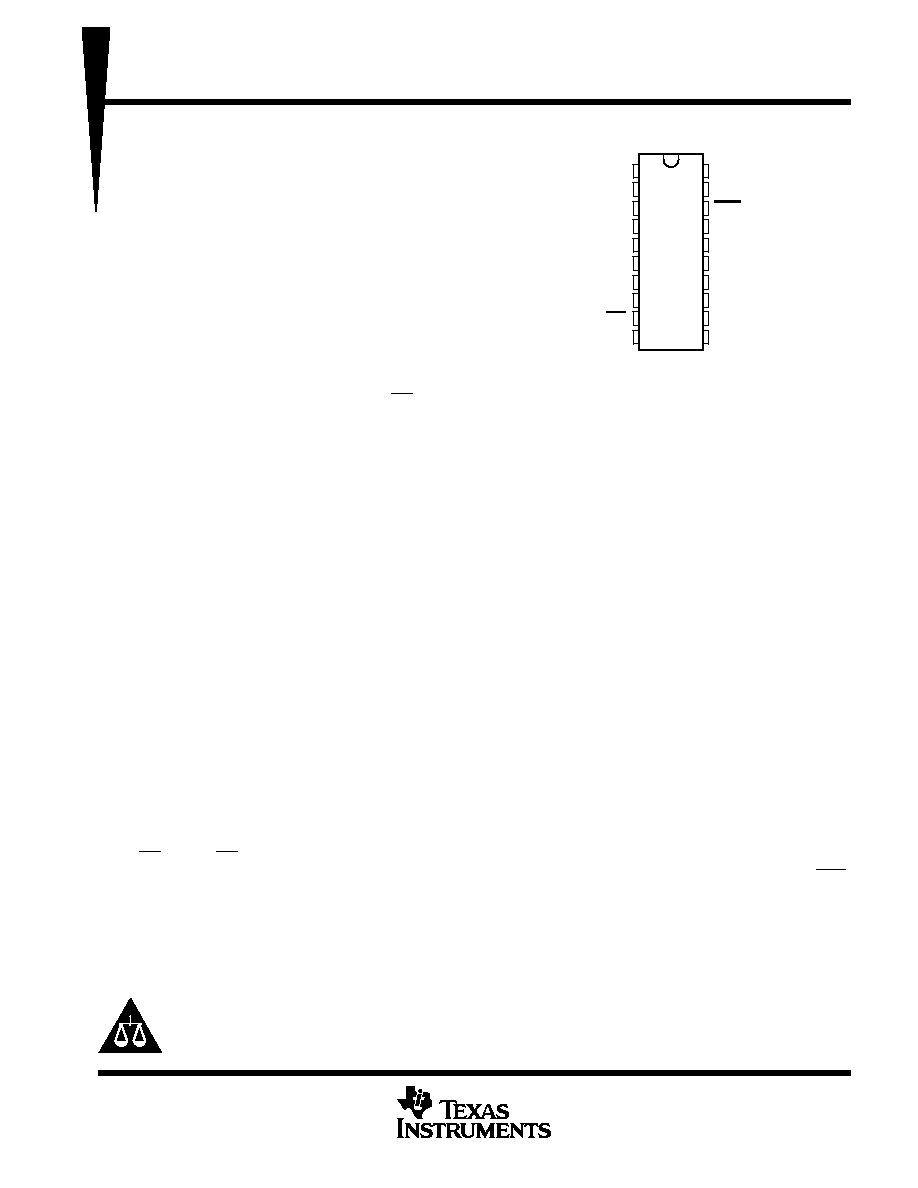
Packaged in Standard Plastic 300-mil DIPs
description
This 80-bit active-element memory is a monolithic
Schottky-clamped transistor-transistor logic
(STTL) array organized as 16 words by 5 bits. A
memory system using the SN74S225 easily can
be expanded in multiples of 48 words or of 10 bits
as shown in Figure 3. The 3-state outputs
controlled by a single output-enable (OE) input
make bus connection and multiplexing easy.
A first-in, first-out (FIFO) memory is a storage device that allows data to be written into and read from its array
at independent data rates. This FIFO is designed to process data at rates from dc to 10 MHz in a bit-parallel
format, word by word.
Reading or writing is done independently, utilizing separate asynchronous data clocks. Data can be written into
the array on the low-to-high transition of either load-clock (CLKA, CLKB) input. Data can be read out of the array
on the low-to-high transition of the unload-clock (UNCK IN) input (normally high). Writing data into the FIFO can
be accomplished in one of two ways:
D
In applications not requiring a gated clock control, best results are achieved by applying the clock input to
one of the clocks while tying the other clock input high.
D
In applications needing a gated clock, the load clock (gate control) must be high for the FIFO to load on the
next clock pulse.
CLKA and CLKB can be used interchangeably for either clock gate control or clock input.
Status of the SN74S225 is provided by three outputs. The input-ready (IR) output monitors the status of the last
word location and signifies when the memory is full. This output is high whenever the memory is available to
accept any data. The unload-clock (UNCK OUT) output also monitors the last word location. This output
generates a low-logic-level pulse (synchronized to the internal clock pulse) when the location is vacant. The third
status output, output ready (OR), is high when the first word location contains valid data and UNCK IN is high.
When UNCK IN goes low, OR will go low and stay low until new valid data is in the first word position. The first
word location is defined as the location from which data is provided to the outputs.
The data outputs are noninverted with respect to the data inputs and are 3-state, with a common control input
(OE). When OE is low, the data outputs are enabled to function as totem-pole outputs. A high logic level forces
each data output to a high-impedance state while all other inputs and outputs remain active.The clear (CLR)
input invalidates all data stored in the memory array by clearing the control logic and setting OR to a low logic
level on the high-to-low transition of a low-active pulse.
The SN74S225 is characterized for operation from 0
∞
C to 70
∞
C.
Copyright
©
1998, Texas Instruments Incorporated
PRODUCTION DATA information is current as of publication date.
Products conform to specifications per the terms of Texas Instruments
standard warranty. Production processing does not necessarily include
testing of all parameters.
1
2
3
4
5
6
7
8
9
10
20
19
18
17
16
15
14
13
12
11
CLKA
IR
UNCK OUT
D0
D1
D2
D3
D4
OE
GND
V
CC
CLKB
CLR
OR
UNCK IN
Q0
Q1
Q2
Q3
Q4
N PACKAGE
(TOP VIEW)
Please be aware that an important notice concerning availability, standard warranty, and use in critical applications of
Texas Instruments semiconductor products and disclaimers thereto appears at the end of this data sheet.
SN74S225
16
◊
5 ASYNCHRONOUS FIRST-IN, FIRST-OUT MEMORY
WITH 3-STATE OUTPUTS
SDLS207B ≠ SEPTEMBER 1976 ≠ REVISED APRIL 1998
2
POST OFFICE BOX 655303
∑
DALLAS, TEXAS 75265
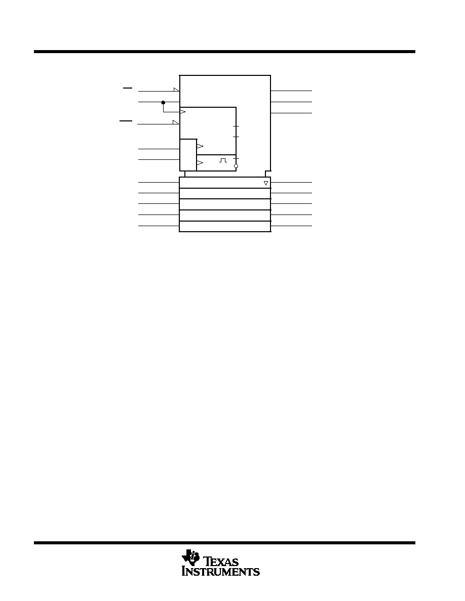
logic symbol
EN6
9
4D
4
D0
Q0
15
5
D1
Q1
14
6
D2
Q2
13
7
D3
Q3
12
8
D4
Q4
11
Z1
16
UNCK IN
FIFO 16
◊
5
OE
6
CT = 0
18
CLR
UNCK OUT
3
2
IR
2
5, 2
OR
17
1, 3
1
CLKA
19
CLKB
3≠
2+
2
&
CTR
G2
G3
C4
Z5
CT < 16
CT > 0
1
This symbol is in accordance with ANSI/IEEE Standard 91-1984 and IEC Publication 617-12.
SN74S225
16
◊
5 ASYNCHRONOUS FIRST
-IN, FIRST
-OUT MEMOR
Y
WITH 3-ST
A
TE OUTPUTS
SDLS207B
≠ SEPTEMBER 1976 ≠ REVISED APRIL 1998
3
POST
OFFICE BOX 655303
∑
DALLAS, TEXAS 75265
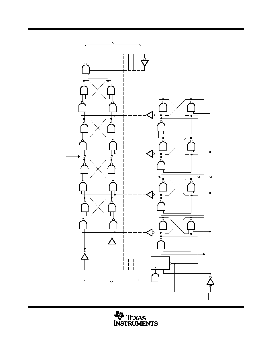
D0
D1
D2
D3
D4
CLKA
CLKB
UNCK
IR
CLR
OUT
Q0
Q1
Q2
Q3
Q4
OE
OR
UNCK
IN
Data Inputs
Data Outputs
4
5
6
7
8
1
19
3
2
18
C1
1D
R
Word 16
(last word)
Word 1
(first word)
Word 2
Word 15
Words 3 ≠ 14
Same as 2 or 15
Same as D10
Same as Q0
15
14
13
12
11
9
17
16
functional block diagram
SN74S225
16
◊
5 ASYNCHRONOUS FIRST-IN, FIRST-OUT MEMORY
WITH 3-STATE OUTPUTS
SDLS207B ≠ SEPTEMBER 1976 ≠ REVISED APRIL 1998
4
POST OFFICE BOX 655303
∑
DALLAS, TEXAS 75265
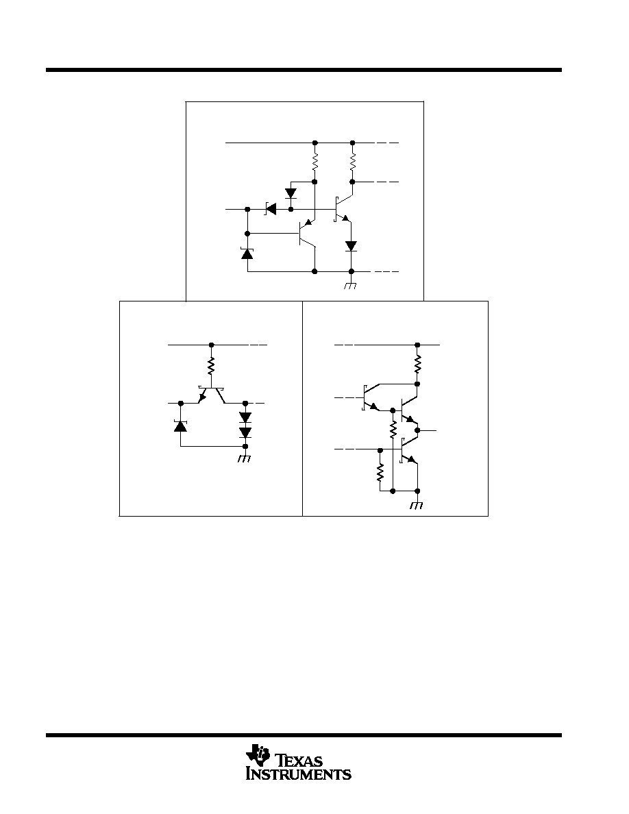
schematics of inputs and outputs
VCC
Input
EQUIVALENT OF ALL INPUTS
EXCEPT DATA INPUTS
VCC
Input
EQUIVALENT OF
DATA INPUTS
58
NOM
VCC
Output
TYPICAL OF
ALL OUTPUTS
absolute maximum ratings over operating free-air temperature range (unless otherwise noted)
Supply voltage range, V
CC
(see Note 1)
≠0.5 V to 7 V
. . . . . . . . . . . . . . . . . . . . . . . . . . . . . . . . . . . . . . . . . . . . . .
Input voltage range, V
I
≠0.5 V to 5.5 V
. . . . . . . . . . . . . . . . . . . . . . . . . . . . . . . . . . . . . . . . . . . . . . . . . . . . . . . . . . . . .
Off-state output voltage range
≠0.5 V to 5.5 V
. . . . . . . . . . . . . . . . . . . . . . . . . . . . . . . . . . . . . . . . . . . . . . . . . . . . . .
Package thermal impedance,
JA
(see Note 2)
67
∞
C/W
. . . . . . . . . . . . . . . . . . . . . . . . . . . . . . . . . . . . . . . . . . . . .
Storage temperature range, T
stg
≠65
∞
C to 150
∞
C
. . . . . . . . . . . . . . . . . . . . . . . . . . . . . . . . . . . . . . . . . . . . . . . . . . .
Stresses beyond those listed under "absolute maximum ratings" may cause permanent damage to the device. These are stress ratings only, and
functional operation of the device at these or any other conditions beyond those indicated under "recommended operating conditions" is not
implied. Exposure to absolute-maximum-rated conditions for extended periods may affect device reliability.
NOTES:
1. All voltage values are with respect to GND.
2. The package thermal impedance is calculated in accordance with JESD 51, except for through-hole packages, which use a trace
length of zero.
SN74S225
16
◊
5 ASYNCHRONOUS FIRST-IN, FIRST-OUT MEMORY
WITH 3-STATE OUTPUTS
SDLS207B ≠ SEPTEMBER 1976 ≠ REVISED APRIL 1998
5
POST OFFICE BOX 655303
∑
DALLAS, TEXAS 75265
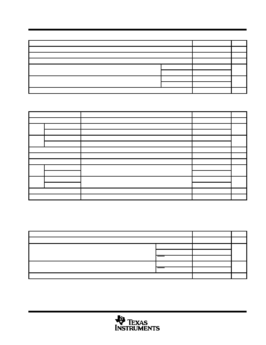
recommended operating conditions
MIN
NOM
MAX
UNIT
VCC
Supply voltage
4.75
5
5.25
V
VIH
High-level input voltage
2
V
VIL
Low-level input voltage
0.8
V
IOH
High level output current
Q outputs
≠6.5
mA
IOH
High-level output current
All other outputs
≠3.2
mA
IOL
Low level output current
Q outputs
16
mA
IOL
Low-level output current
All other outputs
8
mA
TA
Operating free-air temperature
0
70
∞
C
electrical characteristics over recommended operating free-air temperature range (unless
otherwise noted)
PARAMETER
TEST CONDITIONS
MIN
TYP
MAX
UNIT
VIK
VCC = 4.75 V,
II = ≠18 mA
≠1.2
V
VOH
Q outputs
VCC = 4.75 V,
IOL = ≠6.5 mA
2.4
2.9
V
VOH
All others
VCC = 4.75 V,
IOL = ≠3.2 mA
2.4
2.9
V
VOL
Q outputs
VCC = 4.75 V,
IOL = 16 mA
0.35
0.5
V
VOL
All others
VCC = 4.75 V,
IOL = 8 mA
0.35
0.5
V
IOZH
VCC = 5.25 V,
VO = 2.4 V
50
µ
A
IOZL
VCC = 5.25 V,
VO = 0.5 V
≠50
µ
A
II
VCC = 5.25 V,
VI = 5.5 V
1
mA
IIH
Data
VCC = 5 25 V
VI = 2 7 V
40
µ
A
IIH
All others
VCC = 5.25 V,
VI = 2.7 V
25
µ
A
IIL
Data
VCC = 5 25 V
VI = 0 5 V
≠1
mA
IIL
All others
VCC = 5.25 V,
VI = 0.5 V
≠0.25
mA
IOS
VCC = 5.25 V,
VO = 0
≠30
≠100
mA
ICCß
VCC = 5.25 V
80
120
mA
All typical values are at VCC = 5 V, TA = 25
∞
C.
Duration of the short circuit should not exceed one second.
ß ICC is measured with all inputs grounded and the outputs open.
timing requirements over recommended operating conditions (unless otherwise noted) (see
Figure 1)
MIN
NOM
MAX
UNIT
fclock
Clock frequency
10
MHz
CLKA or CLKB high
25
tw
Pulse duration
UNCK IN low
7
ns
CLR low
40
t
Set p time before CLKA
or CLKB
Data (see Note 3)
≠20
ns
tsu
Setup time before CLKA
or CLKB
CLR inactive
25
ns
th
Hold time after CLKA
or CLKB
70
ns
NOTE 3: Data must be set up within 20 ns after the load-clock positive transition.