TPS75201-EP, TPS75215-EP, TPS75218-EP, TPS75225-EP, TPS75233-EP WITH RESET
TPS75401-EP, '75415-EP, '75418-EP, '75425-EP, '75433-EP WITH POWER GOOD
FAST-TRANSIENT-RESPONSE 2-A LOW-DROPOUT VOLTAGE REGULATORS
SGLS165 APRIL 2003
1
POST OFFICE BOX 655303
·
DALLAS, TEXAS 75265
D
Controlled Baseline
One Assembly/Test Site, One Fabrication
Site
D
Enhanced Diminishing Manufacturing
Sources (DMS) Support
D
Enhanced Product-Change Notification
D
Qualification Pedigree
D
2-A Low-Dropout Voltage Regulator
D
Available in 1.5-V, 1.8-V, 2.5-V, 3.3-V Fixed
Output and Adjustable Versions
D
Open Drain Power-On Reset With 100-ms
Delay (TPS752xx)
D
Open Drain Power-Good (PG) Status
Output (TPS754xx)
D
Dropout Voltage Typically 210 mV at 2 A
(TPS75233)
Component qualification in accordance with JEDEC and industry
standards to ensure reliable operation over the specified
temperature range. This includes, but is not limited to, Highly
Accelerated Stress Test (HAST) or biased 85/85, temperature
cycle, autoclave or unbiased HAST, electromigration, bond
intermetallic life, and mold compound life. Such qualification
testing should not be viewed as justifying use of this component
beyond specified performance and environmental limits.
D
Ultralow 75-
µ
A Typical Quiescent Current
D
Fast Transient Response
D
2% Tolerance Over Specified Conditions
for Fixed-Output Versions
D
20-Pin TSSOP (PWP) PowerPAD
Package
D
Thermal Shutdown Protection
description
The TPS752xx and TPS754xx are low dropout regulators with integrated power-on reset and power good (PG)
functions respectively. These devices are capable of supplying 2 A of output current with a dropout of 210 mV
(TPS75233, TPS75433). Quiescent current is 75
µ
A at full load and drops down to 1
µ
A when the device is disabled.
TPS752xx and TPS754xx are designed to have fast transient response for larger load current changes.
Because the PMOS device behaves as a low-value resistor, the dropout voltage is very low (typically 210 mV at an
output current of 2 A for the TPS75x33) and is directly proportional to the output current. Additionally, since the
PMOS pass element is a voltage-driven device, the quiescent current is very low and independent of output loading
(typically 75
µ
A over the full range of output current, 1 mA to 2 A). These two key specifications yield a significant
improvement in operating life for battery-powered systems.
The device is enabled when the EN pin is connected to a low-level input voltage. This LDO family also features a
sleep mode; applying a TTL high signal to EN (enable) shuts down the regulator, reducing the quiescent current
to 1
µ
A at T
J
= 25
°
C.
The RESET (SVS, POR, or power on reset) output of the TPS752xx initiates a reset in microcomputer and
microprocessor systems in the event of an undervoltage condition. An internal comparator in the TPS752xx
monitors the output voltage of the regulator to detect an undervoltage condition on the regulated output voltage.
When the output reaches 95% of its regulated voltage, RESET goes to a high-impedance state after a 100-ms delay.
RESET goes to a logic-low state when the regulated output voltage is pulled below 95% (i.e., over load condition)
of its regulated voltage.
Copyright
2003, Texas Instruments Incorporated
PRODUCTION DATA information is current as of publication date.
Products conform to specifications per the terms of Texas Instruments
standard warranty. Production processing does not necessarily include
testing of all parameters.
PowerPAD is a trademark of Texas Instruments.
Please be aware that an important notice concerning availability, standard warranty, and use in critical applications of
Texas Instruments semiconductor products and disclaimers thereto appears at the end of this data sheet.
1
2
3
4
5
6
7
8
9
10
20
19
18
17
16
15
14
13
12
11
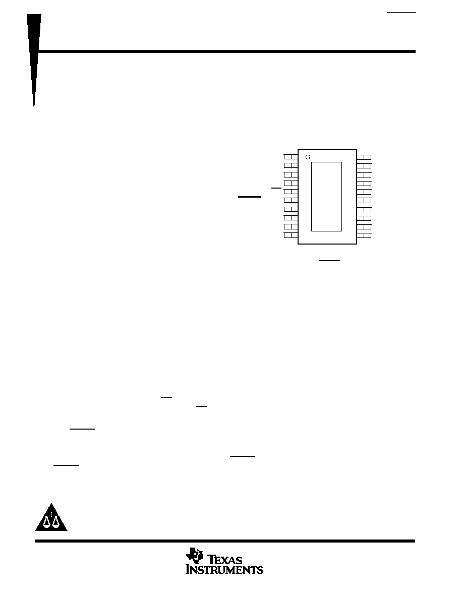
PWP PACKAGE
(TOP VIEW)
GND/HEATSINK
NC
IN
IN
EN
RESETor PG
FB/SENSE
OUTPUT
OUTPUT
GND/HEATSINK
GND/HEATSINK
NC
NC
GND
NC
NC
NC
NC
NC
GND/HEATSINK
NC No internal connection
PG is on the TPS754xx and RESET is on the TPS752xx
TPS75201-EP, TPS75215-EP, TPS75218-EP, TPS75225-EP, TPS75233-EP WITH RESET
TPS75401-EP, '75415-EP, '75418-EP, '75425-EP, '75433-EP WITH POWER GOOD
FAST-TRANSIENT-RESPONSE 2-A LOW-DROPOUT VOLTAGE REGULATORS
SGLS165 APRIL 2003
2
POST OFFICE BOX 655303
·
DALLAS, TEXAS 75265
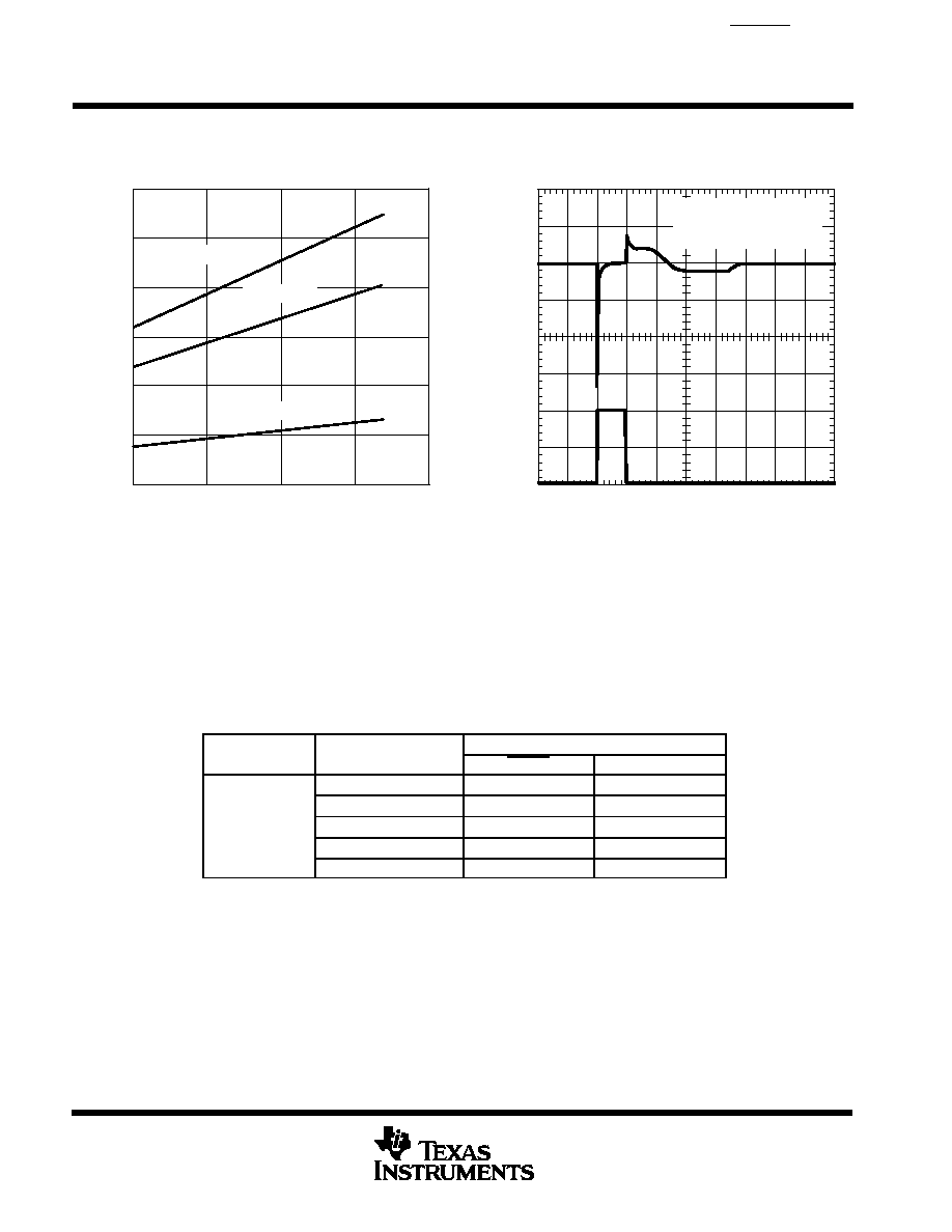
TJ Junction Temperature
°
C
40
10
110
60
Dropout V
oltage
mV
V
DO
TPS75x33
DROPOUT VOLTAGE
vs
JUNCTION TEMPERATURE
300
160
250
200
150
100
50
0
IO = 0.5 A
IO = 1.5 A
IO = 2 A
t Time ms
TPS75x33
LOAD TRANSIENT RESPONSE
I
Output Current
A
O
V
O
Change in
Output V
oltage
mV
150
3
2
1
4
5
7
6
8
9
10
0
0
0
50
50
IL=2 A
CL=100
µ
F (Tantalum)
VO=3.3 V
100
2
1
description (continued)
The TPS754xx has a power good terminal (PG) as an active high, open drain output, which can be used to
implement a power-on reset or a low-battery indicator.
The TPS752xx or the TPS754xx are offered in 1.5-V, 1.8-V, 2.5-V, and 3.3-V fixed-voltage versions and in an
adjustable version (programmable over the range of 1.5 V to 5 V). Output voltage tolerance is specified as a
maximum of 2% over line, load, and temperature ranges. The TPS752xx and the TPS754xx families are available
in 20 pin TSSOP (PWP) packages.
AVAILABLE OPTIONS/ORDERING INFORMATION
TJ
OUTPUT VOLTAGE
TSSOP (PWP)
TJ
OUTPUT VOLTAGE
(TYP)
RESET
PG
3.3 V
TPS75233QPWPEP
TPS75433QPWPEP
2.5 V
TPS75225QPWPEP
TPS75425QPWPEP
40
°
C to 125
°
C
1.8 V
TPS75218QPWPEP
TPS75418QPWPEP
40 C to 125 C
1.5 V
TPS75215QPWPEP
TPS75415QPWPEP
Adjustable 1.5 V to 5 V
TPS75201QPWPEP
TPS75401QPWPEP
The TPS75x01 is programmable using an external resistor divider (see application information). The
PWP package is available taped and reeled. Add an R suffix to the device type (e.g.,
TPS75201QPWPREP) to indicate tape and reel.
Product preview
TPS75201-EP, TPS75215-EP, TPS75218-EP, TPS75225-EP, TPS75233-EP WITH RESET
TPS75401-EP, '75415-EP, '75418-EP, '75425-EP, '75433-EP WITH POWER GOOD
FAST-TRANSIENT-RESPONSE 2-A LOW-DROPOUT VOLTAGE REGULATORS
SGLS165 APRIL 2003
3
POST OFFICE BOX 655303
·
DALLAS, TEXAS 75265
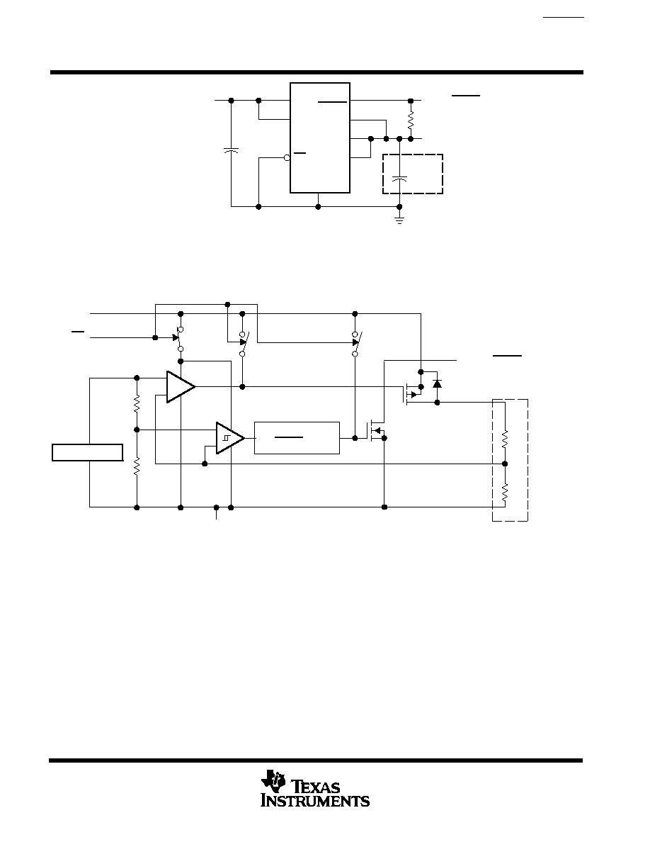
See application information section for capacitor selection details.
PG or
RESET
OUT
OUT
4
3
5
IN
IN
EN
GND
17
6
8
9
VI
0.22
µ
F
PG or RESET Output
VO
47
µ
F
+
CO
SENSE
7
Figure 1. Typical Application Configuration (For Fixed Output Options)
functional block diagram--adjustable version
100 ms Delay
(for RESET Option)
_
+
Vref = 1.1834 V
OUT
FB
EN
GND
PG or RESET
_
+
IN
R1
R2
External to the device
TPS75201-EP, TPS75215-EP, TPS75218-EP, TPS75225-EP, TPS75233-EP WITH RESET
TPS75401-EP, '75415-EP, '75418-EP, '75425-EP, '75433-EP WITH POWER GOOD
FAST-TRANSIENT-RESPONSE 2-A LOW-DROPOUT VOLTAGE REGULATORS
SGLS165 APRIL 2003
4
POST OFFICE BOX 655303
·
DALLAS, TEXAS 75265
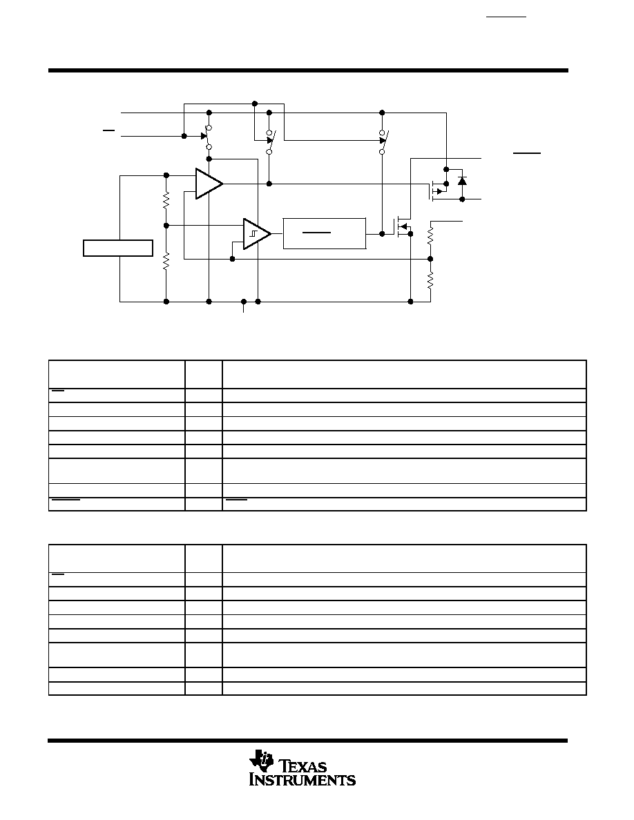
functional block diagram--fixed-voltage version
_
+
Vref = 1.1834 V
OUT
EN
GND
R1
R2
PG or RESET
_
+
IN
SENSE
100 ms Delay
(for RESET Option)
Terminal Functions (TPS752xx)
TERMINAL
I/O
DESCRIPTION
NAME
NO.
I/O
DESCRIPTION
EN
5
I
Enable Input
FB/SENSE
7
I
Feedback input voltage for adjustable device (sense input for fixed-voltage option)
GND
17
Regulator ground
GND/HEATSINK
1, 10, 11, 20
Ground/heatsink
IN
3, 4
I
Input voltage
NC
2, 12, 13, 14,
15, 16, 18, 19
No connection
OUTPUT
8, 9
O
Regulated output voltage
RESET
6
O
Reset output
Terminal Functions (TPS754xx)
TERMINAL
I/O
DESCRIPTION
NAME
NO.
I/O
DESCRIPTION
EN
5
I
Enable Input
FB/SENSE
7
I
Feedback input voltage for adjustable device (sense input for fixed-voltage option)
GND
17
Regulator ground
GND/HEATSINK
1, 10, 11, 20
Ground/heatsink
IN
3, 4
I
Input voltage
NC
2, 12, 13, 14,
15, 16, 18, 19
No connection
OUTPUT
8, 9
O
Regulated output voltage
PG
6
O
Power good output

TPS75201-EP, TPS75215-EP, TPS75218-EP, TPS75225-EP, TPS75233-EP WITH RESET
TPS75401-EP, '75415-EP, '75418-EP, '75425-EP, '75433-EP WITH POWER GOOD
FAST-TRANSIENT-RESPONSE 2-A LOW-DROPOUT VOLTAGE REGULATORS
SGLS165 APRIL 2003
5
POST OFFICE BOX 655303
·
DALLAS, TEXAS 75265
TPS752xx RESET timing diagram
ÎÎ
ÎÎ
ÎÎ
ÎÎ
ÎÎ
ÎÎ
ÎÎ
ÎÎ
ÎÎ
ÎÎ
VI
Vres
(see Note A)
Vres
t
t
t
VO
Threshold
Voltage
RESET
Output
100 ms
Delay
100 ms
Delay
Output
Undefined
Output
Undefined
VIT +(see Note B)
VIT (see Note B)
VIT (see Note B)
VIT +(see Note B)
Less than 5% of the
output voltage
NOTES: A. Vres is the minimum input voltage for a valid RESET. The symbol Vres is not currently listed within EIA or JEDEC standards
for semiconductor symbology.
B. VIT Trip voltage is typically 5% lower than the output voltage (95%VO) VIT to VIT+ is the hysteresis voltage.