 | –≠–ª–µ–∫—Ç—Ä–æ–Ω–Ω—ã–π –∫–æ–º–ø–æ–Ω–µ–Ω—Ç: 8302002SA | –°–∫–∞—á–∞—Ç—å:  PDF PDF  ZIP ZIP |
SN54ALS374A, SN54AS374, SN74ALS374A, SN74AS374
OCTAL D-TYPE EDGE-TRIGGERED FLIP-FLOPS
WITH 3-STATE OUTPUTS
SDAS167C ≠ APRIL 1982 ≠ REVISED NOVEMBER 1999
1
POST OFFICE BOX 655303
∑
DALLAS, TEXAS 75265
D
D-Type Flip-Flops in a Single Package With
3-State Bus Driving True Outputs
D
Full Parallel Access for Loading
D
Buffered Control Inputs
D
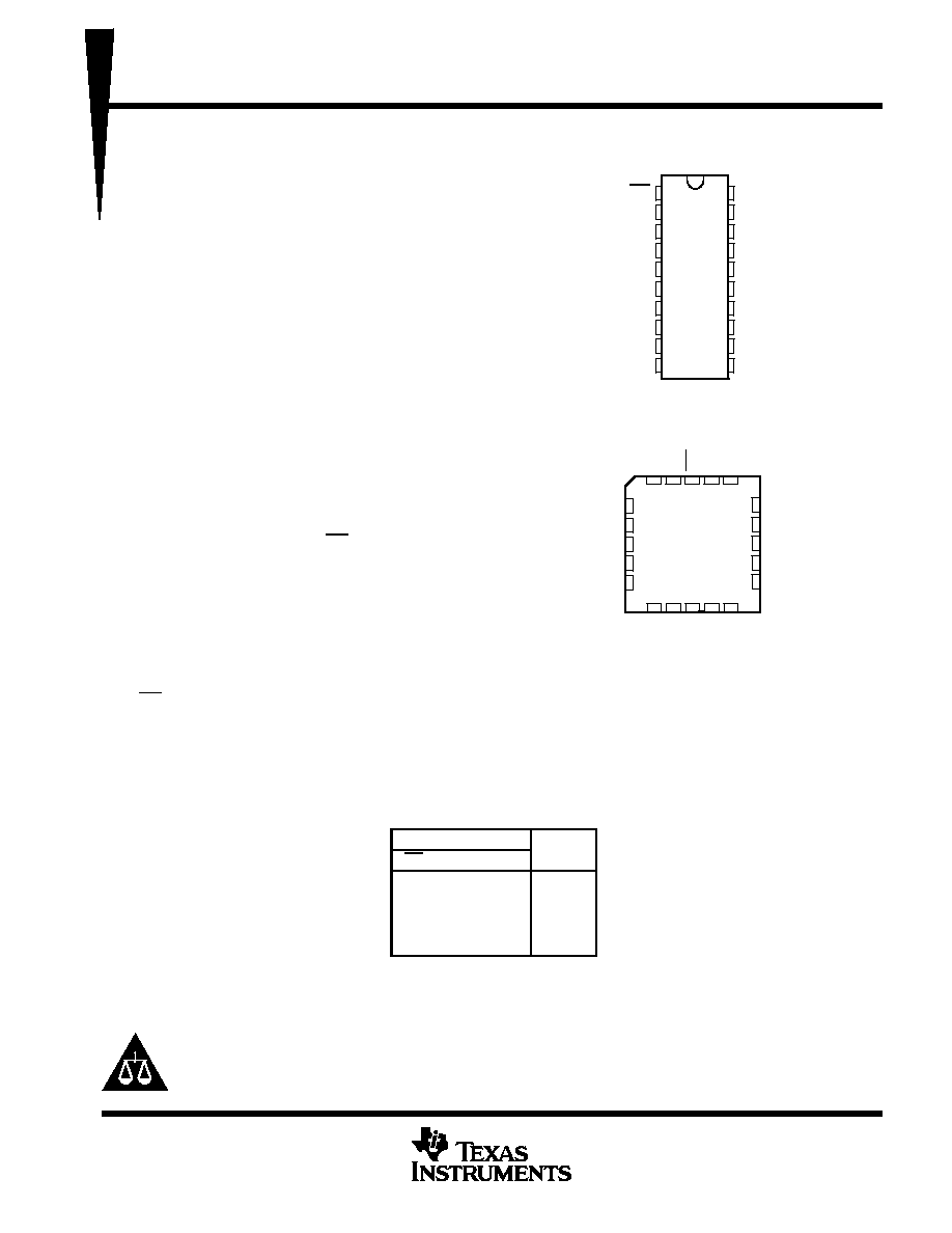
Package Options Include Plastic
Small-Outline (DW) Packages, Ceramic
Chip Carriers (FK), and Standard Plastic (N)
and Ceramic (J) DIPs
description
These octal D-type edge-triggered flip-flops
feature 3-state outputs designed specifically for
driving highly capacitive or relatively
low-impedance loads. They are particularly
suitable for implementing buffer registers, I/O
ports, bidirectional bus drivers, and working
registers.
On the positive transition of the clock (CLK) input,
the Q outputs are set to the logic levels set up at
the data (D) inputs.
A buffered output-enable (OE) input places the
eight outputs in either a normal logic state (high or
low logic levels) or the high-impedance state. In
the high-impedance state, the outputs neither
load nor drive the bus lines significantly. The
high-impedance state and the increased drive
provide the capability to drive bus lines without
interface or pullup components.
OE does not affect internal operations of the flip-flops. Old data can be retained or new data can be entered
while the outputs are in the high-impedance state.
The SN54ALS374A and SN54AS374 are characterized for operation over the full military temperature range
of ≠55
∞
C to 125
∞
C. The SN74ALS374A and SN74AS374 are characterized for operation from 0
∞
C to 70
∞
C.
FUNCTION TABLE
(each flip-flop)
INPUTS
OUTPUT
OE
CLK
D
Q
L
H
H
L
L
L
L
H or L
X
Q0
H
X
X
Z
Copyright
©
1999, Texas Instruments Incorporated
PRODUCTION DATA information is current as of publication date.
Products conform to specifications per the terms of Texas Instruments
standard warranty. Production processing does not necessarily include
testing of all parameters.
Please be aware that an important notice concerning availability, standard warranty, and use in critical applications of
Texas Instruments semiconductor products and disclaimers thereto appears at the end of this data sheet.
1
2
3
4
5
6
7
8
9
10
20
19
18
17
16
15
14
13
12
11
OE
1Q
1D
2D
2Q
3Q
3D
4D
4Q
GND
V
CC
8Q
8D
7D
7Q
6Q
6D
5D
5Q
CLK
SN54ALS374A, SN54AS374 . . . J PACKAGE
SN74ALS374A, SN74AS374 . . . DW OR N PACKAGE
(TOP VIEW)
3
2 1 20 19
9 10 11 12 13
4
5
6
7
8
18
17
16
15
14
8D
7D
7Q
6Q
6D
2D
2Q
3Q
3D
4D
SN54ALS374A, SN54AS374 . . . FK PACKAGE
(TOP VIEW)
1D
1Q
OE
5Q
5D
8Q
4Q
GND
CLK
V
CC
On products compliant to MIL-PRF-38535, all parameters are tested
unless otherwise noted. On all other products, production
processing does not necessarily include testing of all parameters.
SN54ALS374A, SN54AS374, SN74ALS374A, SN74AS374
OCTAL D-TYPE EDGE-TRIGGERED FLIP-FLOPS
WITH 3-STATE OUTPUTS
SDAS167C ≠ APRIL 1982 ≠ REVISED NOVEMBER 1999
2
POST OFFICE BOX 655303
∑
DALLAS, TEXAS 75265
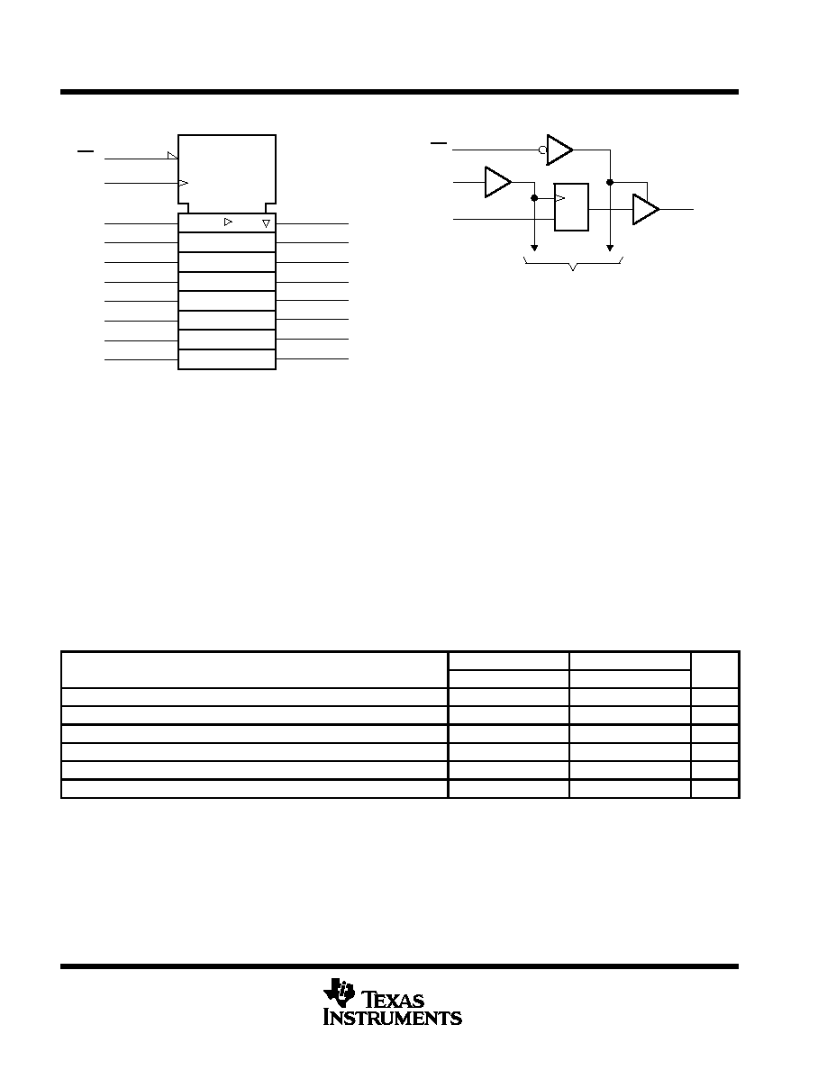
logic symbol
This symbol is in accordance with ANSI/IEEE Std 91-1984 and
IEC Publication 617-12.
C1
OE
EN
1
11
CLK
1D
3
1D
4
2D
7
3D
8
4D
5Q
12
6Q
15
7Q
16
8Q
19
13
5D
14
6D
17
7D
18
8D
1Q
2
2Q
5
3Q
6
4Q
9
logic diagram (positive logic)
1D
CLK
1Q
2
11
3
1
1D
OE
C1
To Seven Other Channels
absolute maximum ratings over operating free-air temperature range (unless otherwise noted)
Supply voltage range, V
CC
≠0.5 V to 7 V
. . . . . . . . . . . . . . . . . . . . . . . . . . . . . . . . . . . . . . . . . . . . . . . . . . . . . . . . . .
Input voltage range, V
I
≠0.5 V to 7 V
. . . . . . . . . . . . . . . . . . . . . . . . . . . . . . . . . . . . . . . . . . . . . . . . . . . . . . . . . . . . . .
Voltage applied to a disabled 3-state output
≠0.5 V to 5.5 V
. . . . . . . . . . . . . . . . . . . . . . . . . . . . . . . . . . . . . . . . . .
Package thermal impedance,
JA
(see Note 1): DW package
58
∞
C/W
. . . . . . . . . . . . . . . . . . . . . . . . . . . . . . . . .
N package
69
∞
C/W
. . . . . . . . . . . . . . . . . . . . . . . . . . . . . . . . . . .
Storage temperature range, T
stg
≠65
∞
C to 150
∞
C
. . . . . . . . . . . . . . . . . . . . . . . . . . . . . . . . . . . . . . . . . . . . . . . . . . .
Stresses beyond those listed under "absolute maximum ratings" may cause permanent damage to the device. These are stress ratings only, and
functional operation of the device at these or any other conditions beyond those indicated under "recommended operating conditions" is not
implied. Exposure to absolute-maximum-rated conditions for extended periods may affect device reliability.
NOTE 1: The package thermal impedance is calculated in accordance with JESD 51.
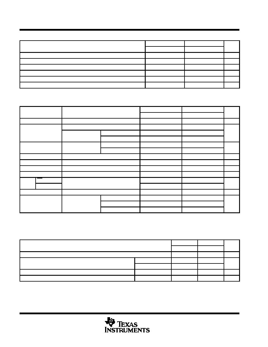
recommended operating conditions
SN54ALS374A
SN74ALS374A
UNIT
MIN
NOM
MAX
MIN
NOM
MAX
UNIT
VCC
Supply voltage
4.5
5
5.5
4.5
5
5.5
V
VIH
High-level input voltage
2
2
V
VIL
Low-level input voltage
0.7
0.8
V
IOH
High-level output current
≠1
≠2.6
mA
IOL
Low-level output current
12
24
mA
TA
Operating free-air temperature
≠55
125
0
70
∞
C

SN54ALS374A, SN54AS374, SN74ALS374A, SN74AS374
OCTAL D-TYPE EDGE-TRIGGERED FLIP-FLOPS
WITH 3-STATE OUTPUTS
SDAS167C ≠ APRIL 1982 ≠ REVISED NOVEMBER 1999
3
POST OFFICE BOX 655303
∑
DALLAS, TEXAS 75265
electrical characteristics over recommended operating free-air temperature range (unless
otherwise noted)
PARAMETER
TEST CONDITIONS
SN54ALS374A
SN74ALS374A
UNIT
PARAMETER
TEST CONDITIONS
MIN
TYP
MAX
MIN
TYP
MAX
UNIT
VIK
VCC = 4.5 V,
II = ≠18 mA
≠1.5
≠1.5
V
VCC = 4.5 V to 5.5 V,
IOH = ≠0.4 mA
VCC≠2
VCC≠2
VOH
VCC = 4 5 V
IOH = ≠1 mA
2.4
3.3
V
VCC = 4.5 V
IOH = ≠2.6 mA
2.4
3.2
VOL
VCC = 4 5 V
IOL = 12 mA
0.25
0.4
0.25
0.4
V
VOL
VCC = 4.5 V
IOL = 24 mA
0.35
0.5
V
IOZH
VCC = 5.5 V,
VO = 2.7 V
20
20
µ
A
IOZL
VCC = 5.5 V,
VO = 0.4 V
≠20
≠20
µ
A
II
VCC = 5.5 V,
VI = 7 V
0.1
0.1
mA
IIH
VCC = 5.5 V,
VI = 2.7 V
20
20
µ
A
IIL
VCC = 5.5 V,
VI = 0.4 V
≠0.2
≠0.2
mA
IO
VCC = 5.5 V,
VO = 2.25 V
≠20
≠112
≠30
≠112
mA
Outputs high
11
20
11
19
ICC
VCC = 5.5 V
Outputs low
19
28
19
28
mA
Outputs disabled
20
31
20
31
All typical values are at VCC = 5 V, TA = 25
∞
C.
The output conditions have been chosen to produce a current that closely approximates one half of the true short-circuit output current, IOS.
timing requirements over recommended operating free-air temperature range (unless otherwise
noted)
SN54ALS374A
SN74ALS374A
UNIT
MIN
MAX
MIN
MAX
UNIT
fclock
Clock frequency
30
35
MHz
tw
Pulse duration
CLK high or low
16.5
14
ns
tsu
Setup time
Data before CLK
10
10
ns
th
Hold time
Data after CLK
4
0
ns
switching characteristics over recommended operating conditions (unless otherwise noted
(see Figure 3)
PARAMETER
FROM
TO
SN54ALS374A
SN74ALS374A
UNIT
PARAMETER
(INPUT)
(OUTPUT)
MIN
MAX
MIN
MAX
UNIT
fmax
30
35
MHz
tPLH
CLK
Q
3
14
3
12
ns
tPHL
CLK
Q
5
17
5
16
ns
tPZH
OE
Q
3
18
3
17
ns
tPZL
OE
Q
5
21
5
18
ns
tPHZ
OE
Q
1
11
1
10
ns
tPLZ
OE
Q
2
19
2
18
ns
SN54ALS374A, SN54AS374, SN74ALS374A, SN74AS374
OCTAL D-TYPE EDGE-TRIGGERED FLIP-FLOPS
WITH 3-STATE OUTPUTS
SDAS167C ≠ APRIL 1982 ≠ REVISED NOVEMBER 1999
4
POST OFFICE BOX 655303
∑
DALLAS, TEXAS 75265
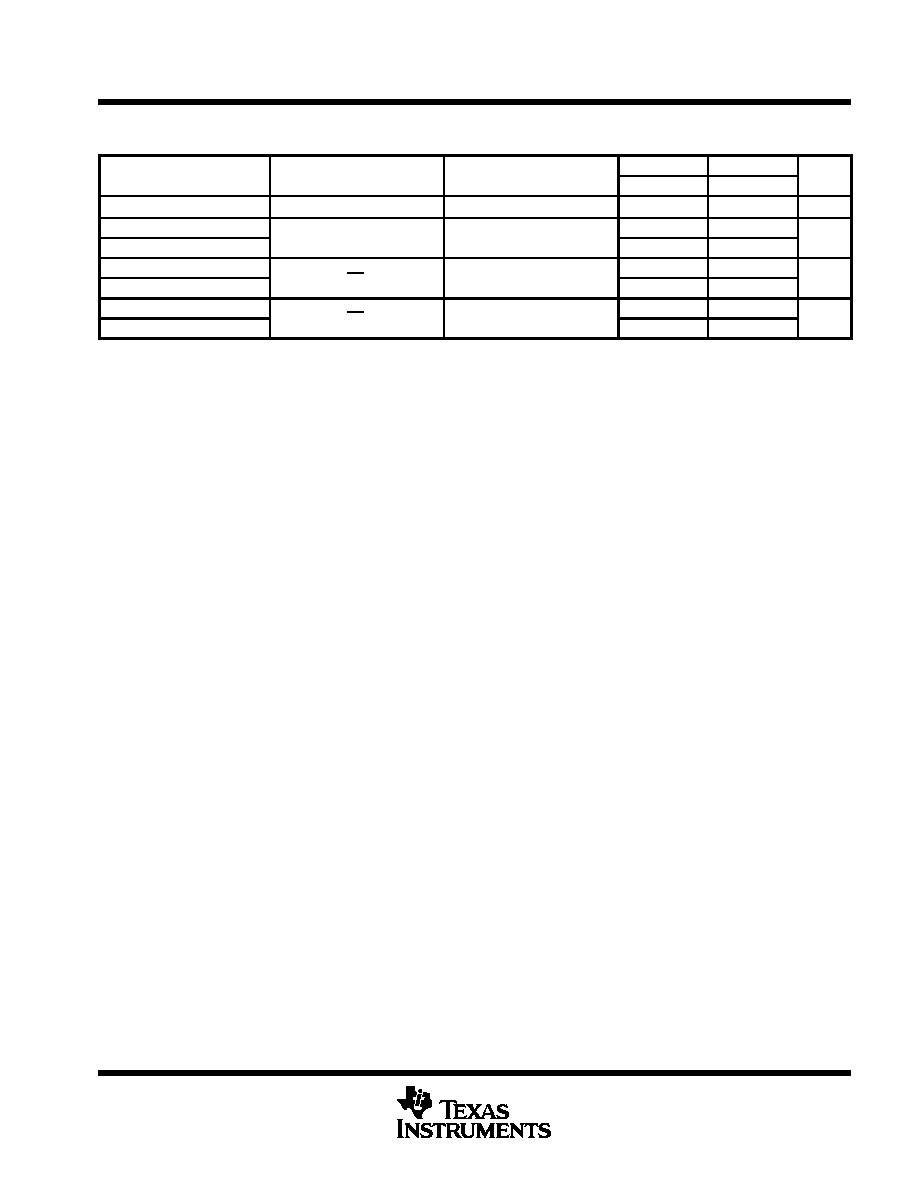
recommended operating conditions
SN54AS374
SN74AS374
UNIT
MIN
NOM
MAX
MIN
NOM
MAX
UNIT
VCC
Supply voltage
4.5
5
5.5
4.5
5
5.5
V
VIH
High-level input voltage
2
2
V
VIL
Low-level input voltage
0.7
0.8
V
IOH
High-level output current
≠12
≠15
mA
IOL
Low-level output current
32
48
mA
TA
Operating free-air temperature
≠55
125
0
70
∞
C
electrical characteristics over recommended operating free-air temperature range (unless
otherwise noted)
PARAMETER
TEST CONDITIONS
SN54AS374
SN74AS374
UNIT
PARAMETER
TEST CONDITIONS
MIN
TYP
MAX
MIN
TYP
MAX
UNIT
VIK
VCC = 4.5 V,
II = ≠18 mA
≠1.2
≠1.2
V
VCC = 4.5 V to 5.5 V,
IOH = ≠2 mA
VCC≠2
VCC≠2
VOH
VCC = 4 5 V
IOH = ≠12 mA
2.4
3.2
V
VCC = 4.5 V
IOH = ≠15 mA
2.4
3.3
VOL
VCC = 4 5 V
IOL = 32 mA
0.29
0.5
V
VOL
VCC = 4.5 V
IOL = 48 mA
0.34
0.5
V
IOZH
VCC = 5.5 V,
VO = 2.7 V
50
50
µ
A
IOZL
VCC = 5.5 V,
VO = 0.4 V
≠50
≠50
µ
A
II
VCC = 5.5 V,
VI = 7 V
0.1
0.1
mA
IIH
VCC = 5.5 V,
VI = 2.7 V
20
20
µ
A
IIL
OE, CLK
VCC = 5 5 V
VI = 0 4 V
≠0.5
≠0.5
mA
IIL
Data
VCC = 5.5 V,
VI = 0.4 V
≠3
≠2
mA
IO
VCC = 5.5 V,
VO = 2.25 V
≠30
≠112
≠30
≠112
mA
Outputs high
77
120
77
120
ICC
VCC = 5.5 V
Outputs low
84
128
84
128
mA
Outputs disabled
84
128
84
128
All typical values are at VCC = 5 V, TA = 25
∞
C.
The output conditions have been chosen to produce a current that closely approximates one half of the true short-circuit output current, IOS.
timing requirements over recommended operating free-air temperature range (unless otherwise
noted)
SN54AS374
SN74AS374
UNIT
MIN
MAX
MIN
MAX
UNIT
fclock
Clock frequency
100*
125
MHz
t
Pulse duration
CLK high
5.5*
4
ns
tw
Pulse duration
CLK low
3*
3
ns
tsu
Setup time
Data before CLK
3*
2
ns
th
Hold time
Data after CLK
3*
2
ns
* On products compliant to MIL-PRF-38535, this parameter is not production tested.
SN54ALS374A, SN54AS374, SN74ALS374A, SN74AS374
OCTAL D-TYPE EDGE-TRIGGERED FLIP-FLOPS
WITH 3-STATE OUTPUTS
SDAS167C ≠ APRIL 1982 ≠ REVISED NOVEMBER 1999
5
POST OFFICE BOX 655303
∑
DALLAS, TEXAS 75265
switching characteristics over recommended operating conditions (unless otherwise noted)
(see Figure 3)
PARAMETER
FROM
TO
SN54AS374
SN74AS374
UNIT
PARAMETER
(INPUT)
(OUTPUT)
MIN
MAX
MIN
MAX
UNIT
fmax
100*
125
MHz
tPLH
CLK
Q
3
11
3
8
ns
tPHL
CLK
Q
4
11.5
4
9
ns
tPZH
OE
Q
2
7
2
6
ns
tPZL
OE
Q
3
11
3
10
ns
tPHZ
OE
Q
2
10
2
6
ns
tPLZ
OE
Q
2
7
2
6
ns
* On products compliant to MIL-PRF-38535, this parameter is not production tested.
SN54ALS374A, SN54AS374, SN74ALS374A, SN74AS374
OCTAL D-TYPE EDGE-TRIGGERED FLIP-FLOPS
WITH 3-STATE OUTPUTS
SDAS167C ≠ APRIL 1982 ≠ REVISED NOVEMBER 1999
6
POST OFFICE BOX 655303
∑
DALLAS, TEXAS 75265
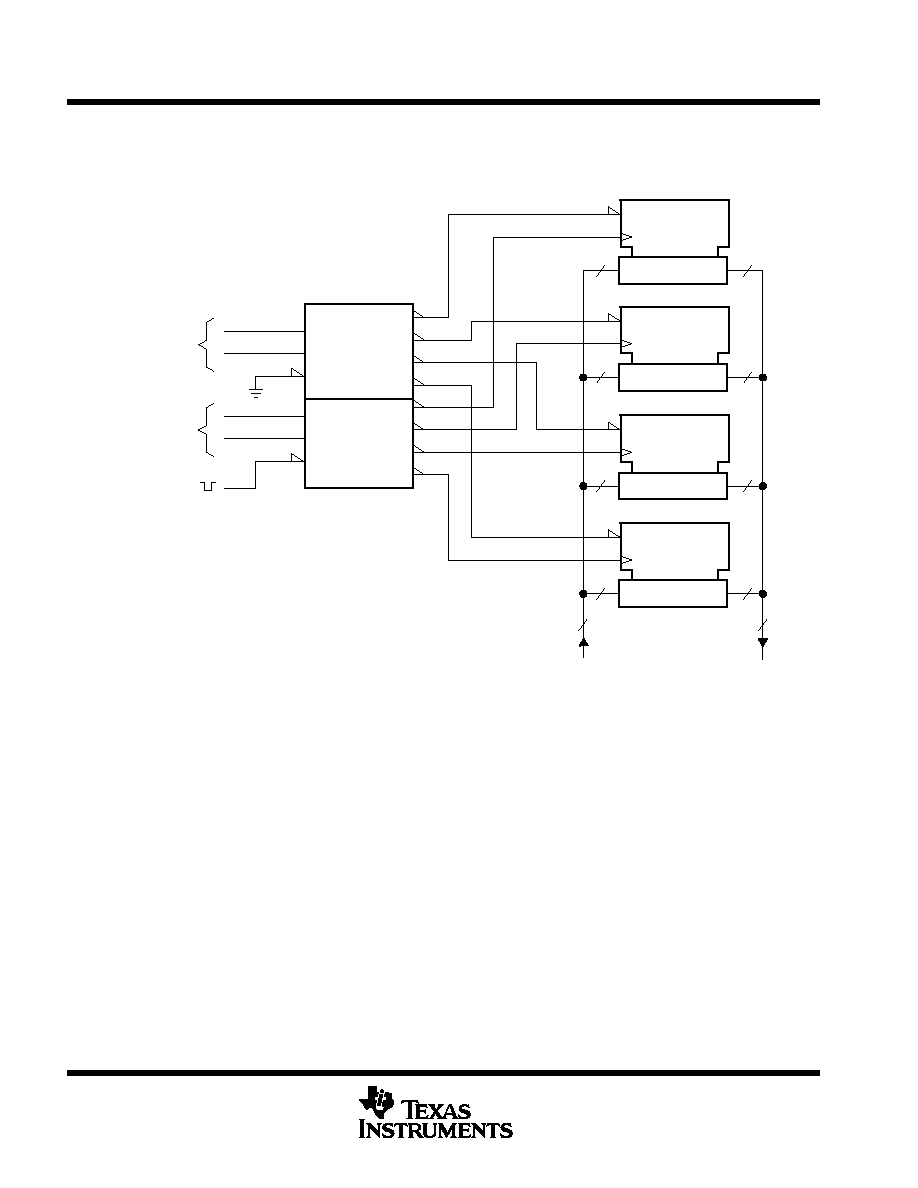
APPLICATION INFORMATION
X/Y
'ALS139
A
B
G
A
B
G
Output-Enable
Select
Input Clock
Select
Clock
1
2
EN
0
1
2
3
8
8
EN
C
Four SN54ALS374A,
SN74ALS374A,
or 'AS374
8
8
EN
C
8
8
EN
C
8
8
EN
C
8
8
Input
Output
Figure 1. Expandable 4-Word by 8-Bit General File Register
SN54ALS374A, SN54AS374, SN74ALS374A, SN74AS374
OCTAL D-TYPE EDGE-TRIGGERED FLIP-FLOPS
WITH 3-STATE OUTPUTS
SDAS167C ≠ APRIL 1982 ≠ REVISED NOVEMBER 1999
7
POST OFFICE BOX 655303
∑
DALLAS, TEXAS 75265
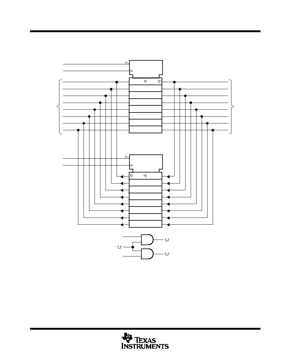
APPLICATION INFORMATION
EN
C1
1D
SN54ALS374A,
SN74ALS374A,
or 'AS374
EN
C1
Bidirectional
Data Bus 1
Bidirectional
Data Bus 2
Output Enable 1
Clock 1
Output Enable 2
Clock 2
H
H
Clock 1
Clock 2
Bus-Exchange
Clock
1D
Clock Circuit for Bus Exchange
SN54ALS374A,
SN74ALS374A,
or 'AS374
Figure 2. Bidirectional Bus Driver
SN54ALS374A, SN54AS374, SN74ALS374A, SN74AS374
OCTAL D-TYPE EDGE-TRIGGERED FLIP-FLOPS
WITH 3-STATE OUTPUTS
SDAS167C ≠ APRIL 1982 ≠ REVISED NOVEMBER 1999
8
POST OFFICE BOX 655303
∑
DALLAS, TEXAS 75265
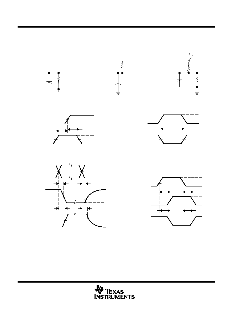
PARAMETER MEASUREMENT INFORMATION
SERIES 54ALS/74ALS AND 54AS/74AS DEVICES
tPHZ
tPLZ
tPHL
tPLH
tPZL
tPZH
tPLH
tPHL
LOAD CIRCUIT FOR
3-STATE OUTPUTS
From Output
Under Test
Test
Point
S1
CL = 50 pF
(see Note A)
7 V
3.5 V
3.5 V
0.3 V
0.3 V
th
tsu
VOLTAGE WAVEFORMS
SETUP AND HOLD TIMES
Timing
Input
Data
Input
3.5 V
3.5 V
0.3 V
0.3 V
High-Level
Pulse
Low-Level
Pulse
tw
VOLTAGE WAVEFORMS
PULSE DURATIONS
Input
Out-of-Phase
Output
(see Note C)
3.5 V
3.5 V
0.3 V
0.3 V
VOL
VOH
VOH
VOL
Output
Control
Waveform 1
S1 Closed
(see Note B)
Waveform 2
S1 Open
(see Note B)
0 V
VOH
VOL
3.5 V
In-Phase
Output
VOLTAGE WAVEFORMS
PROPAGATION DELAY TIMES
VOLTAGE WAVEFORMS
ENABLE AND DISABLE TIMES, 3-STATE OUTPUTS
VCC
Test
Point
From Output
Under Test
CL = 50 pF
(see Note A)
LOAD CIRCUIT FOR
OPEN-COLLECTOR OUTPUTS
LOAD CIRCUIT FOR
BI-STATE TOTEM-POLE OUTPUTS
From Output
Under Test
Test
Point
CL = 50 pF
(see Note A)
500
500
500
500
VOL + 0.3 V
VOH ≠ 0.3 V
1.3 V
1.3 V
1.3 V
1.3 V
1.3 V
1.3 V
1.3 V
1.3 V
1.3 V
1.3 V
1.3 V
1.3 V
1.3 V
1.3 V
1.3 V
1.3 V
1.3 V
NOTES: A. CL includes probe and jig capacitance.
B. Waveform 1 is for an output with internal conditions such that the output is low except when disabled by the output control.
Waveform 2 is for an output with internal conditions such that the output is high except when disabled by the output control.
C. When measuring propagation delay items of 3-state outputs, switch S1 is open.
D. All input pulses have the following characteristics: PRR
1 MHz, tr = tf = 2 ns, duty cycle = 50%.
E. The outputs are measured one at a time with one transition per measurement.
Figure 3. Load Circuits and Voltage Waveforms

IMPORTANT NOTICE
Texas Instruments and its subsidiaries (TI) reserve the right to make changes to their products or to discontinue
any product or service without notice, and advise customers to obtain the latest version of relevant information
to verify, before placing orders, that information being relied on is current and complete. All products are sold
subject to the terms and conditions of sale supplied at the time of order acknowledgement, including those
pertaining to warranty, patent infringement, and limitation of liability.
TI warrants performance of its semiconductor products to the specifications applicable at the time of sale in
accordance with TI's standard warranty. Testing and other quality control techniques are utilized to the extent
TI deems necessary to support this warranty. Specific testing of all parameters of each device is not necessarily
performed, except those mandated by government requirements.
CERTAIN APPLICATIONS USING SEMICONDUCTOR PRODUCTS MAY INVOLVE POTENTIAL RISKS OF
DEATH, PERSONAL INJURY, OR SEVERE PROPERTY OR ENVIRONMENTAL DAMAGE ("CRITICAL
APPLICATIONS"). TI SEMICONDUCTOR PRODUCTS ARE NOT DESIGNED, AUTHORIZED, OR
WARRANTED TO BE SUITABLE FOR USE IN LIFE-SUPPORT DEVICES OR SYSTEMS OR OTHER
CRITICAL APPLICATIONS. INCLUSION OF TI PRODUCTS IN SUCH APPLICATIONS IS UNDERSTOOD TO
BE FULLY AT THE CUSTOMER'S RISK.
In order to minimize risks associated with the customer's applications, adequate design and operating
safeguards must be provided by the customer to minimize inherent or procedural hazards.
TI assumes no liability for applications assistance or customer product design. TI does not warrant or represent
that any license, either express or implied, is granted under any patent right, copyright, mask work right, or other
intellectual property right of TI covering or relating to any combination, machine, or process in which such
semiconductor products or services might be or are used. TI's publication of information regarding any third
party's products or services does not constitute TI's approval, warranty or endorsement thereof.
Copyright
©
1999, Texas Instruments Incorporated