 | –≠–ª–µ–∫—Ç—Ä–æ–Ω–Ω—ã–π –∫–æ–º–ø–æ–Ω–µ–Ω—Ç: 8407001EA | –°–∫–∞—á–∞—Ç—å:  PDF PDF  ZIP ZIP |
1
Data sheet acquired from Harris Semiconductor
SCHS135F
Features
∑ True and Complementary Outputs
∑ Buffered Inputs and Outputs
∑ Fanout (Over Temperature Range)
- Standard Outputs . . . . . . . . . . . . . . . 10 LSTTL Loads
- Bus Driver Outputs . . . . . . . . . . . . . 15 LSTTL Loads
∑ Wide Operating Temperature Range . . . -55
o
C to 125
o
C
∑ Balanced Propagation Delay and Transition Times
∑ Significant Power Reduction Compared to LSTTL
Logic ICs
∑ HC Types
- 2V to 6V Operation
- High Noise Immunity: N
IL
= 30%, N
IH
= 30% of V
CC
at V
CC
= 5V
∑ HCT Types
- 4.5V to 5.5V Operation
- Direct LSTTL Input Logic Compatibility,
V
IL
= 0.8V (Max), V
IH
= 2V (Min)
- CMOS Input Compatibility, I
l
1
µ
A at V
OL
, V
OH
Description
The 'HC75 and 'HCT75 are dual 2-bit bistable transparent
latches. Each one of the 2-bit latches is controlled by
separate Enable inputs (1E and 2E) which are active LOW.
When the Enable input is HIGH data enters the latch and
appears at the Q output. When the Enable input (1E and 2E)
is LOW the output is not affected.
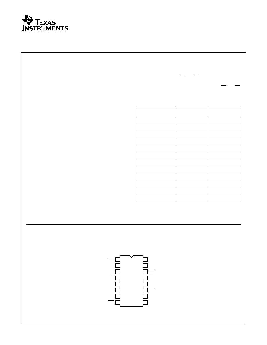
Pinout
CD54HC75, CD54HCT75 (CERDIP)
CD74HC75 (PDIP, SOIC, SOP, TSSOP)
CD74HCT75 (PDIP, SOIC, TSSOP)
TOP VIEW
Ordering Information
PART NUMBER
TEMP. RANGE
(
o
C)
PACKAGE
CD54HC75F3A
-55 to 125
16 Ld CERDIP
CD54HCT75F3A
-55 to 125
16 Ld CERDIP
CD74HC75E
-55 to 125
16 Ld PDIP
CD74HC75M
-55 to 125
16 Ld SOIC
CD74HC75MT
-55 to 125
16 Ld SOIC
CD74HC75M96
-55 to 125
16 Ld SOIC
CD74HC75NSR
-55 to 125
16 Ld SOP
CD74HC75PW
-55 to 125
16 Ld TSSOP
CD74HC75PWR
-55 to 125
16 Ld TSSOP
CD74HCT75E
-55 to 125
16 Ld PDIP
CD74HCT75M
-55 to 125
16 Ld SOIC
CD74HCT75PWT
-55 to 125
16 Ld TSSOP
NOTE: When ordering, use the entire part number. The suffixes 96
and R denote tape and reel. The suffix T denotes a small-quantity
reel of 250.
14
15
16
9
13
12
11
10
1
2
3
4
5
7
6
8
1Q0
1D0
1D1
2E
V
CC
2D0
2Q1
2D1
1Q0
1Q1
1E
GND
2Q0
2Q0
2Q1
1Q1
March 1998 - Revised October 2003
CAUTION: These devices are sensitive to electrostatic discharge. Users should follow proper IC Handling Procedures.
Copyright
©
2003, Texas Instruments Incorporated
CD54HC75, CD74HC75,
CD54HCT75, CD74HCT75
Dual 2-Bit Bistable
Transparent Latch
[ /Title
(CD74
HC75,
CD74
HCT75
)
/Sub-
ject
(Dual
2-Bit
Bistabl
e
2
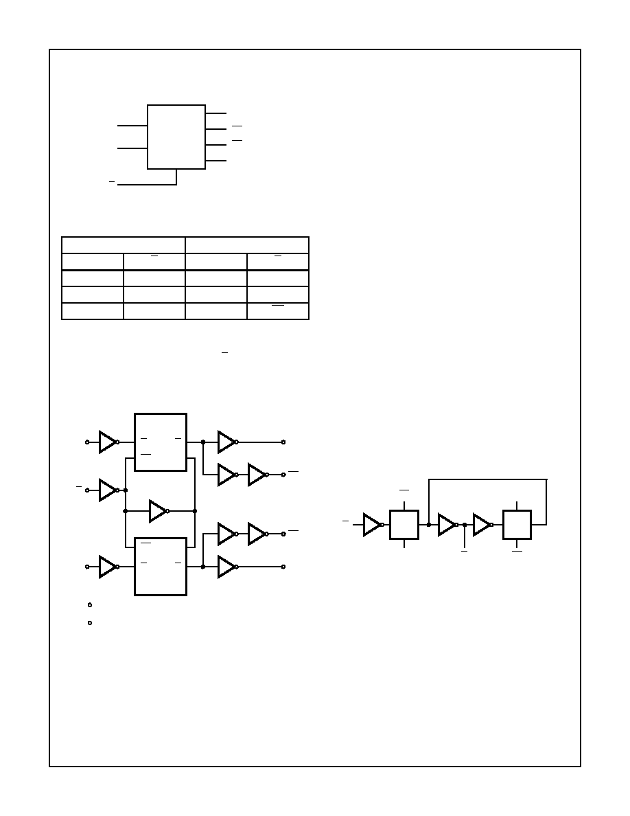
Functional Diagram
Logic Diagram
TRUTH TABLE
INPUTS
OUTPUTS
D
E
Q
Q
L
H
L
H
H
H
H
L
X
L
Q0
Q0
H= High Level
L= Low Level
X= Don't Care
Q0 = The level of Q before the transition of E.
D0
2 (6)
3 (7)
16 (10)
Q1
Q0
D1
13 (4)
E
1 (11)
14 (8)
15 (9)
Q0
Q1
1 OF 2
LATCHES
FIGURE 1. LOGIC DIAGRAM
FIGURE 2. LATCH DETAIL
D0
3 (7)
2 (6)
LATCH 0
Q
D
LE
LE
16 (10)
1 (11)
Q0
Q0
E
13 (4)
LATCH 1
Q
D
LE
LE
D1
14 (8)
Q1
15 (9)
Q1
5
12
GND
V
CC
P
N
LE
LE
Q
P
N
LE
LE
Q
CD54HC75, CD74HC75, CD54HCT75, CD74HCT75
3
Absolute Maximum Ratings
Thermal Information
DC Supply Voltage, V
CC
. . . . . . . . . . . . . . . . . . . . . . . . -0.5V to 7V
DC Input Diode Current, I
IK
For V
I
< -0.5V or V
I
> V
CC
+ 0.5V
. . . . . . . . . . . . . . . . . . . . . .±
20mA
DC Drain Current, per Output, I
O
For -0.5V < V
O
< V
CC
+ 0.5V
. . . . . . . . . . . . . . . . . . . . . . . . . .±
25mA
DC Output Diode Current, I
OK
For V
O
< -0.5V or V
O
> V
CC
+ 0.5V
. . . . . . . . . . . . . . . . . . . .±
20mA
DC Output Source or Sink Current per Output Pin, I
O
For V
O
> -0.5V or V
O
< V
CC
+ 0.5V
. . . . . . . . . . . . . . . . . . . .±
25mA
DC V
CC
or Ground Current, I
CC
. . . . . . . . . . . . . . . . . . . . . . . . .±
50mA
Operating Conditions
Temperature Range, T
A
. . . . . . . . . . . . . . . . . . . . . . -55
o
C to 125
o
C
Supply Voltage Range, V
CC
HC Types . . . . . . . . . . . . . . . . . . . . . . . . . . . . . . . . . . . . .2V to 6V
HCT Types . . . . . . . . . . . . . . . . . . . . . . . . . . . . . . . . .4.5V to 5.5V
DC Input or Output Voltage, V
I
, V
O
. . . . . . . . . . . . . . . . . 0V to V
CC
Input Rise and Fall Time
2V . . . . . . . . . . . . . . . . . . . . . . . . . . . . . . . . . . . . . . 1000ns (Max)
4.5V. . . . . . . . . . . . . . . . . . . . . . . . . . . . . . . . . . . . . . 500ns (Max)
6V . . . . . . . . . . . . . . . . . . . . . . . . . . . . . . . . . . . . . . . 400ns (Max)
Package Thermal Impedance,
JA
(see Note 1)
E (PDIP) package . . . . . . . . . . . . . . . . . . . . . . . . . . . . . . 67
o
C/W
M (SOIC) package . . . . . . . . . . . . . . . . . . . . . . . . . . . . . . 73
o
C/W
NS (SOP) package . . . . . . . . . . . . . . . . . . . . . . . . . . . . . 64
o
C/W
PW (TSSOP) package . . . . . . . . . . . . . . . . . . . . . . . . . . 108
o
C/W
Maximum Junction Temperature (Hermetic Package or Die) . . . 175
o
C
Maximum Junction Temperature (Plastic Package) . . . . . . . . 150
o
C
Maximum Storage Temperature Range . . . . . . . . . .-65
o
C to 150
o
C
Maximum Lead Temperature (Soldering 10s) . . . . . . . . . . . . . 300
o
C
(SOIC - Lead Tips Only)
CAUTION: Stresses above those listed in "Absolute Maximum Ratings" may cause permanent damage to the device. This is a stress only rating and operation
of the device at these or any other conditions above those indicated in the operational sections of this specification is not implied.
NOTE:
1. The package thermal impedance is calculated in accordance with JESD 51-7.
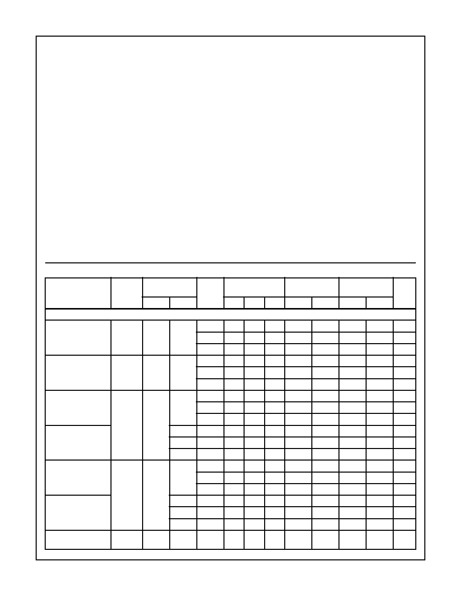
DC Electrical Specifications
PARAMETER
SYMBOL
TEST
CONDITIONS
V
CC
(V)
25
o
C
-40
o
C TO 85
o
C
-55
o
C TO 125
o
C
UNITS
V
I
(V)
I
O
(mA)
MIN
TYP
MAX
MIN
MAX
MIN
MAX
HC TYPES
High Level Input
Voltage
V
IH
-
-
2
1.5
-
-
1.5
-
1.5
-
V
4.5
3.15
-
-
3.15
-
3.15
-
V
6
4.2
-
-
4.2
-
4.2
-
V
Low Level Input
Voltage
V
IL
-
-
2
-
-
0.5
-
0.5
-
0.5
V
4.5
-
-
1.35
-
1.35
-
1.35
V
6
-
-
1.8
-
1.8
-
1.8
V
High Level Output
Voltage
CMOS Loads
V
OH
V
IH
or
V
IL
-0.02
2
1.9
-
-
1.9
-
1.9
-
V
4.5
4.4
-
-
4.4
-
4.4
-
V
6
5.9
-
-
5.9
-
5.9
-
V
High Level Output
Voltage
TTL Loads
-
-
-
-
-
-
-
-
-
V
-4
4.5
3.98
-
-
3.84
-
3.7
-
V
-5.2
6
5.48
-
-
5.34
-
5.2
-
V
Low Level Output
Voltage
CMOS Loads
V
OL
V
IH
or
V
IL
0.02
2
-
-
0.1
-
0.1
-
0.1
V
4.5
-
-
0.1
-
0.1
-
0.1
V
6
-
-
0.1
-
0.1
-
0.1
V
Low Level Output
Voltage
TTL Loads
-
-
-
-
-
-
-
-
-
V
4
4.5
-
-
0.26
-
0.33
-
0.4
V
5.2
6
-
-
0.26
-
0.33
-
0.4
V
Input Leakage
Current
I
I
V
CC
or
GND
-
6
-
-
±
0.1
-
±
1
-
±
1
µ
A
CD54HC75, CD74HC75, CD54HCT75, CD74HCT75
4
Quiescent Device
Current
I
CC
V
CC
or
GND
0
6
-
-
4
-
40
-
80
µ
A
HCT TYPES
High Level Input
Voltage
V
IH
-
-
4.5 to
5.5
2
-
-
2
-
2
-
V
Low Level Input
Voltage
V
IL
-
-
4.5 to
5.5
-
-
0.8
-
0.8
-
0.8
V
High Level Output
Voltage
CMOS Loads
V
OH
V
IH
or
V
IL
- 0.02
4.5
4.4
-
-
4.4
-
4.4
-
V
High Level Output
Voltage
TTL Loads
-4
4.5
3.98
-
-
3.84
-
3.7
-
V
Low Level Output
Voltage CMOS Loads
V
OL
V
IH
or
V
IL
0.02
4.5
-
-
0.1
-
0.1
-
0.1
V
Low Level Output
Voltage
TTL Loads
4
4.5
-
-
0.26
-
0.33
-
0.4
V
Input Leakage
Current
I
I
V
CC
and
GND
-
5.5
-
±
0.1
-
±
1
-
±
1
µ
A
Quiescent Device
Current
I
CC
V
CC
or
GND
0
5.5
-
-
4
-
40
-
80
µ
A
Additional Quiescent
Device Current Per
Input Pin: 1 Unit Load
I
CC
(Note 2)
V
CC
- 2.1
-
4.5 to
5.5
-
100
360
-
450
-
490
µ
A
NOTE:
2. For dual-supply systems theoretical worst case (V
I
= 2.4V, V
CC
= 5.5V) specification is 1.8mA.
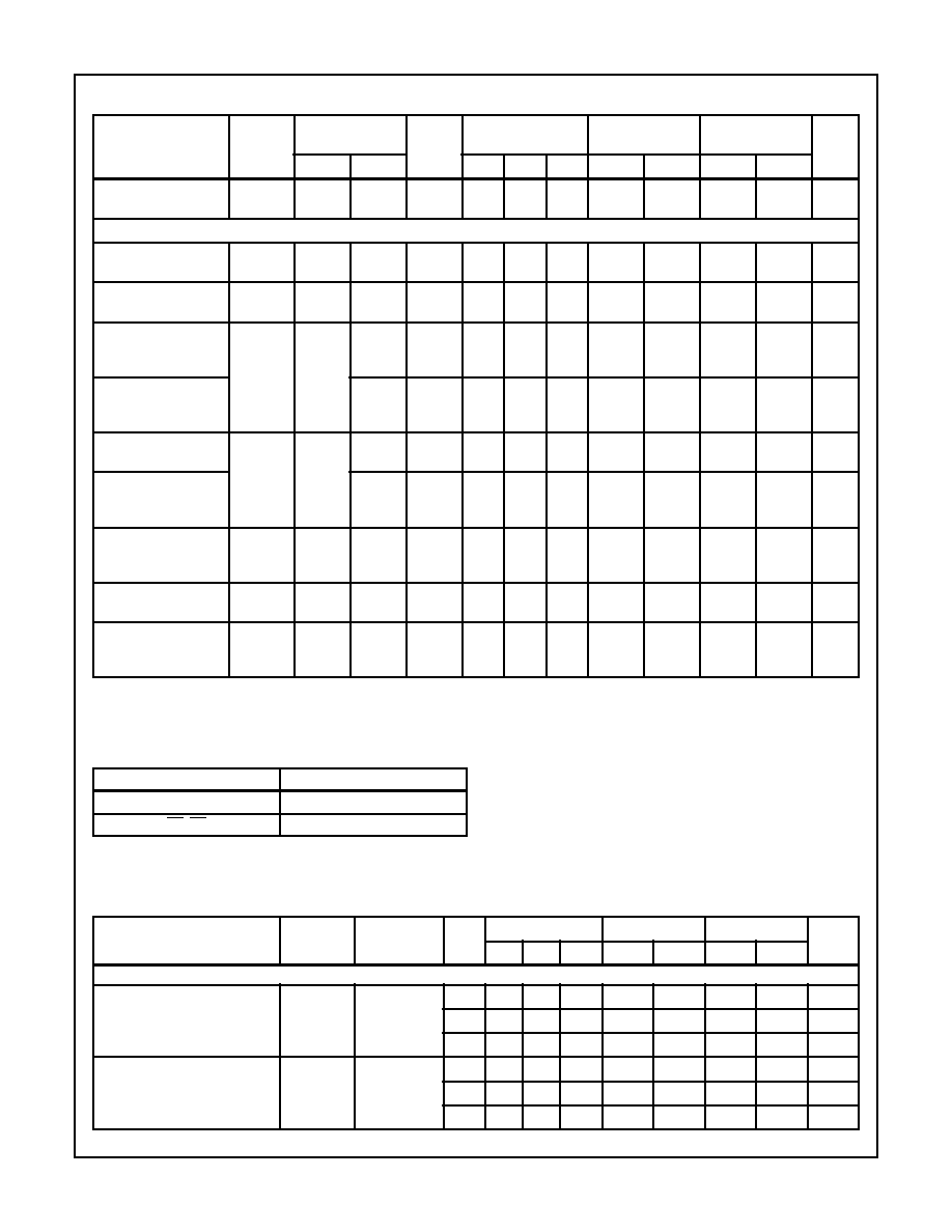
DC Electrical Specifications
(Continued)
PARAMETER
SYMBOL
TEST
CONDITIONS
V
CC
(V)
25
o
C
-40
o
C TO 85
o
C
-55
o
C TO 125
o
C
UNITS
V
I
(V)
I
O
(mA)
MIN
TYP
MAX
MIN
MAX
MIN
MAX
HCT Input Loading Table
INPUT
UNIT LOADS
D0, D1
0.8
1E, 2E
1.2
NOTE: Unit Load is
I
CC
limit specified in DC Electrical Specifica-
tions table, e.g., 360
µ
A max at 25
o
C.
Prerequisite For Switching Specifications
PARAMETER
SYMBOL
TEST
CONDITIONS
V
CC
(V)
25
o
C
-40
o
C TO 85
o
C
-55
o
C TO 125
o
C
UNITS
MIN
TYP
MAX
MIN
MAX
MIN
MAX
HC TYPES
Pulse Width Enable Input
t
W
-
2
80
-
-
100
-
120
-
ns
4.5
16
-
-
20
-
24
-
ns
6
14
-
-
17
-
20
-
ns
Setup Time D to Enable
t
SU
-
2
60
-
-
75
-
90
-
ns
4.5
12
-
-
15
-
18
-
ns
6
10
-
-
13
-
15
-
ns
CD54HC75, CD74HC75, CD54HCT75, CD74HCT75

5
Hold Time Enable to D
t
H
-
2
3
-
-
3
-
3
-
ns
4.5
3
-
-
3
-
3
-
ns
6
3
-
-
3
-
3
-
ns
HCT TYPES
Pulse Width Enable Input
t
W
-
4.5
16
-
-
20
-
24
-
ns
Setup Time D to Enable
t
SU
-
4.5
12
-
-
15
-
18
-
ns
Hold Time Enable to D
t
H
-
4.5
3
-
-
3
-
3
-
ns
Switching Specifications
Input t
r
, t
f
= 6ns
PARAMETER
SYMBOL
TEST
CONDITIONS
V
CC
(V)
25
o
C
-40
o
C TO 85
o
C
-55
o
C TO 125
o
C
UNITS
MIN
TYP
MAX
MIN
MAX
MIN
MAX
HC TYPES
Propagation Delay,
Data to Q
t
PLH
, t
PHL
C
L
= 50pF
2
-
-
110
-
140
-
165
ns
C
L
= 50pF
4.5
-
-
22
-
28
-
33
ns
C
L
= 15pF
5
-
9
-
-
-
-
-
ns
C
L
= 50pF
6
-
-
19
-
24
-
28
ns
Propagation Delay,
Data to Q
t
PLH
, t
PHL
C
L
= 50pF
2
-
-
130
-
165
-
195
ns
C
L
= 50pF
4.5
-
-
26
-
33
-
39
ns
C
L
= 15pF
5
-
10
-
-
-
-
-
ns
C
L
= 50pF
6
-
-
22
-
28
-
33
ns
Propagation Delay,
Enable to Q
t
PLH
, t
PHL
C
L
= 50pF
2
-
-
130
-
165
-
195
ns
C
L
= 50pF
4.5
-
-
26
-
33
-
39
ns
C
L
= 15pF
5
-
10
-
-
-
-
-
ns
C
L
= 50pF
6
-
-
22
-
28
-
33
ns
Propagation Delay,
Enable to Q
t
PLH
, t
PHL
C
L
= 50pF
2
-
-
130
-
165
-
195
ns
C
L
= 50pF
4.5
-
-
26
-
33
-
39
ns
C
L
= 15pF
5
-
11
-
-
-
-
-
ns
C
L
= 50pF
6
-
-
22
-
28
-
33
ns
Output Transition Time
t
TLH
, t
THL
C
L
= 50pF
2
-
-
75
-
95
-
110
ns
C
L
= 50pF
4.5
-
-
15
-
19
-
22
ns
C
L
= 50pF
6
-
-
13
-
16
-
19
ns
Input Capacitance
C
I
-
-
-
-
10
-
10
-
10
pF
Power Dissipation Capacitance
(Notes 3, 4)
C
PD
-
5
-
46
-
-
-
-
-
pF
HCT TYPES
Propagation Delay,
Data to Q
t
PLH
, t
PHL
C
L
= 50pF
4.5
-
-
28
-
35
-
42
ns
C
L
= 15pF
5
-
11
-
-
-
-
-
ns
Propagation Delay,
Data to Q
t
PLH
, t
PHL
C
L
= 50pF
4.5
-
-
28
-
35
-
42
ns
C
L
= 15pF
5
-
11
-
-
-
-
-
ns
Propagation Delay,
Enable to Q
t
PLH
, t
PHL
C
L
= 50pF
4.5
-
-
28
-
35
-
42
ns
C
L
= 15pF
5
11
-
-
-
-
-
ns
Prerequisite For Switching Specifications
(Continued)
PARAMETER
SYMBOL
TEST
CONDITIONS
V
CC
(V)
25
o
C
-40
o
C TO 85
o
C
-55
o
C TO 125
o
C
UNITS
MIN
TYP
MAX
MIN
MAX
MIN
MAX
CD54HC75, CD74HC75, CD54HCT75, CD74HCT75
6
Propagation Delay,
Enable to Q
t
PLH
, t
PHL
C
L
= 50pF
4.5
-
-
30
-
38
-
45
ns
C
L
= 15pF
5
-
12
-
-
-
-
-
ns
Output Transition Time
t
TLH
, t
THL
C
L
= 50pF
4.5
-
-
15
-
19
-
22
ns
Input Capacitance
C
I
-
-
-
-
10
-
10
-
10
pF
Power Dissipation Capacitance
(Notes 3, 4)
C
PD
-
5
-
46
-
-
-
-
-
pF
NOTES:
3. C
PD
is used to determine the dynamic power consumption, per latch.
4. P
D
= V
CC
2
f
i
(C
PD
+ C
L
) where f
i
= input frequency, C
L
= output load capacitance, V
CC
= supply voltage.
Switching Specifications
Input t
r
, t
f
= 6ns (Continued)
PARAMETER
SYMBOL
TEST
CONDITIONS
V
CC
(V)
25
o
C
-40
o
C TO 85
o
C
-55
o
C TO 125
o
C
UNITS
MIN
TYP
MAX
MIN
MAX
MIN
MAX
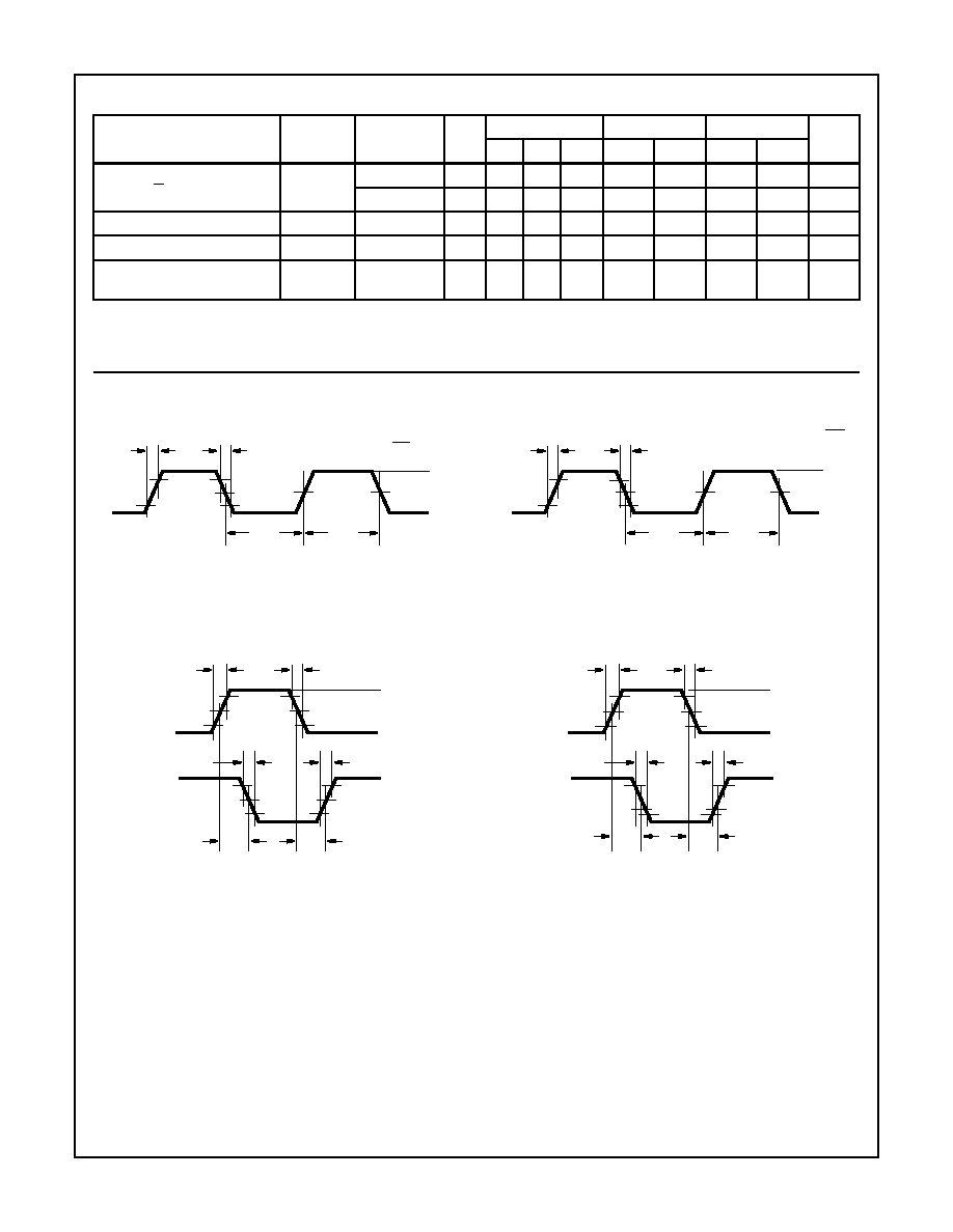
Test Circuits and Waveforms
NOTE: Outputs should be switching from 10% V
CC
to 90% V
CC
in
accordance with device truth table. For f
MAX
, input duty cycle = 50%.
FIGURE 3. HC CLOCK PULSE RISE AND FALL TIMES AND
PULSE WIDTH
NOTE: Outputs should be switching from 10% V
CC
to 90% V
CC
in
accordance with device truth table. For f
MAX
, input duty cycle = 50%.
FIGURE 4. HCT CLOCK PULSE RISE AND FALL TIMES AND
PULSE WIDTH
FIGURE 5. HC AND HCU TRANSITION TIMES AND PROPAGA-
TION DELAY TIMES, COMBINATION LOGIC
FIGURE 6. HCT TRANSITION TIMES AND PROPAGATION
DELAY TIMES, COMBINATION LOGIC
CLOCK
90%
50%
10%
GND
V
CC
t
r
C
L
t
f
C
L
50%
50%
t
WL
t
WH
10%
t
WL
+ t
WH
=
f
CL
I
CLOCK
2.7V
1.3V
0.3V
GND
3V
t
r
C
L
= 6ns
t
f
C
L
= 6ns
1.3V
1.3V
t
WL
t
WH
0.3V
t
WL
+ t
WH
=
fC
L
I
t
PHL
t
PLH
t
THL
t
TLH
90%
50%
10%
50%
10%
INVERTING
OUTPUT
INPUT
GND
V
CC
t
r
= 6ns
t
f
= 6ns
90%
t
PHL
t
PLH
t
THL
t
TLH
2.7V
1.3V
0.3V
1.3V
10%
INVERTING
OUTPUT
INPUT
GND
3V
t
r
= 6ns
t
f
= 6ns
90%
CD54HC75, CD74HC75, CD54HCT75, CD74HCT75
7
FIGURE 7. HC SETUP TIMES, HOLD TIMES, REMOVAL TIME,
AND PROPAGATION DELAY TIMES FOR EDGE
TRIGGERED SEQUENTIAL LOGIC CIRCUITS
FIGURE 8. HCT SETUP TIMES, HOLD TIMES, REMOVAL TIME,
AND PROPAGATION DELAY TIMES FOR EDGE
TRIGGERED SEQUENTIAL LOGIC CIRCUITS
Test Circuits and Waveforms
(Continued)
t
r
C
L
t
f
C
L
GND
V
CC
GND
V
CC
50%
90%
10%
GND
CLOCK
INPUT
DATA
INPUT
OUTPUT
SET, RESET
OR PRESET
V
CC
50%
50%
90%
10%
50%
90%
t
REM
t
PLH
t
SU(H)
t
TLH
t
THL
t
H(L)
t
PHL
IC
C
L
50pF
t
SU(L)
t
H(H)
t
r
C
L
t
f
C
L
GND
3V
GND
3V
1.3V
2.7V
0.3V
GND
CLOCK
INPUT
DATA
INPUT
OUTPUT
SET, RESET
OR PRESET
3V
1.3V
1.3V
1.3V
90%
10%
1.3V
90%
t
REM
t
PLH
t
SU(H)
t
TLH
t
THL
t
H(L)
t
PHL
IC
C
L
50pF
t
SU(L)
1.3V
t
H(H)
1.3V
CD54HC75, CD74HC75, CD54HCT75, CD74HCT75
PACKAGING INFORMATION
Orderable Device
Status
(1)
Package
Type
Package
Drawing
Pins Package
Qty
Eco Plan
(2)
Lead/Ball Finish
MSL Peak Temp
(3)
5962-9075801MEA
ACTIVE
CDIP
J
16
1
TBD
Call TI
Level-NC-NC-NC
8407001EA
ACTIVE
CDIP
J
16
1
TBD
Call TI
Level-NC-NC-NC
CD54HC75F3A
ACTIVE
CDIP
J
16
1
TBD
Call TI
Level-NC-NC-NC
CD54HCT75F3A
ACTIVE
CDIP
J
16
1
TBD
Call TI
Level-NC-NC-NC
CD74HC75E
ACTIVE
PDIP
N
16
25
Pb-Free
(RoHS)
CU NIPDAU
Level-NC-NC-NC
CD74HC75M
ACTIVE
SOIC
D
16
40
Green (RoHS &
no Sb/Br)
CU NIPDAU
Level-1-260C-UNLIM
CD74HC75M96
ACTIVE
SOIC
D
16
2500 Green (RoHS &
no Sb/Br)
CU NIPDAU
Level-1-260C-UNLIM
CD74HC75M96E4
ACTIVE
SOIC
D
16
2500 Green (RoHS &
no Sb/Br)
CU NIPDAU
Level-1-260C-UNLIM
CD74HC75MT
ACTIVE
SOIC
D
16
250
Green (RoHS &
no Sb/Br)
CU NIPDAU
Level-1-260C-UNLIM
CD74HC75MTE4
ACTIVE
SOIC
D
16
250
Green (RoHS &
no Sb/Br)
CU NIPDAU
Level-1-260C-UNLIM
CD74HC75NSR
ACTIVE
SO
NS
16
2000 Green (RoHS &
no Sb/Br)
CU NIPDAU
Level-1-260C-UNLIM
CD74HC75NSRE4
ACTIVE
SO
NS
16
2000 Green (RoHS &
no Sb/Br)
CU NIPDAU
Level-1-260C-UNLIM
CD74HC75PW
ACTIVE
TSSOP
PW
16
90
Green (RoHS &
no Sb/Br)
CU NIPDAU
Level-1-260C-UNLIM
CD74HC75PWE4
ACTIVE
TSSOP
PW
16
90
Green (RoHS &
no Sb/Br)
CU NIPDAU
Level-1-260C-UNLIM
CD74HC75PWR
ACTIVE
TSSOP
PW
16
2000 Green (RoHS &
no Sb/Br)
CU NIPDAU
Level-1-260C-UNLIM
CD74HC75PWRE4
ACTIVE
TSSOP
PW
16
2000 Green (RoHS &
no Sb/Br)
CU NIPDAU
Level-1-260C-UNLIM
CD74HC75PWT
ACTIVE
TSSOP
PW
16
250
Green (RoHS &
no Sb/Br)
CU NIPDAU
Level-1-260C-UNLIM
CD74HC75PWTE4
ACTIVE
TSSOP
PW
16
250
Green (RoHS &
no Sb/Br)
CU NIPDAU
Level-1-260C-UNLIM
CD74HCT75E
ACTIVE
PDIP
N
16
25
Pb-Free
(RoHS)
CU NIPDAU
Level-NC-NC-NC
CD74HCT75M
ACTIVE
SOIC
D
16
40
Green (RoHS &
no Sb/Br)
CU NIPDAU
Level-1-260C-UNLIM
CD74HCT75ME4
ACTIVE
SOIC
D
16
40
Green (RoHS &
no Sb/Br)
CU NIPDAU
Level-1-260C-UNLIM
(1)
The marketing status values are defined as follows:
ACTIVE: Product device recommended for new designs.
LIFEBUY: TI has announced that the device will be discontinued, and a lifetime-buy period is in effect.
NRND: Not recommended for new designs. Device is in production to support existing customers, but TI does not recommend using this part in
a new design.
PREVIEW: Device has been announced but is not in production. Samples may or may not be available.
OBSOLETE: TI has discontinued the production of the device.
(2)
Eco
Plan
-
The
planned
eco-friendly
classification:
Pb-Free
(RoHS)
or
Green
(RoHS
&
no
Sb/Br)
-
please
check
http://www.ti.com/productcontent
for the latest availability information and additional product content details.
TBD: The Pb-Free/Green conversion plan has not been defined.
Pb-Free (RoHS): TI's terms "Lead-Free" or "Pb-Free" mean semiconductor products that are compatible with the current RoHS requirements
PACKAGE OPTION ADDENDUM
www.ti.com
9-Aug-2005
Addendum-Page 1

for all 6 substances, including the requirement that lead not exceed 0.1% by weight in homogeneous materials. Where designed to be soldered
at high temperatures, TI Pb-Free products are suitable for use in specified lead-free processes.
Green (RoHS & no Sb/Br): TI defines "Green" to mean Pb-Free (RoHS compatible), and free of Bromine (Br) and Antimony (Sb) based flame
retardants (Br or Sb do not exceed 0.1% by weight in homogeneous material)
(3)
MSL, Peak Temp. -- The Moisture Sensitivity Level rating according to the JEDEC industry standard classifications, and peak solder
temperature.
Important Information and Disclaimer:The information provided on this page represents TI's knowledge and belief as of the date that it is
provided. TI bases its knowledge and belief on information provided by third parties, and makes no representation or warranty as to the
accuracy of such information. Efforts are underway to better integrate information from third parties. TI has taken and continues to take
reasonable steps to provide representative and accurate information but may not have conducted destructive testing or chemical analysis on
incoming materials and chemicals. TI and TI suppliers consider certain information to be proprietary, and thus CAS numbers and other limited
information may not be available for release.
In no event shall TI's liability arising out of such information exceed the total purchase price of the TI part(s) at issue in this document sold by TI
to Customer on an annual basis.
PACKAGE OPTION ADDENDUM
www.ti.com
9-Aug-2005
Addendum-Page 2
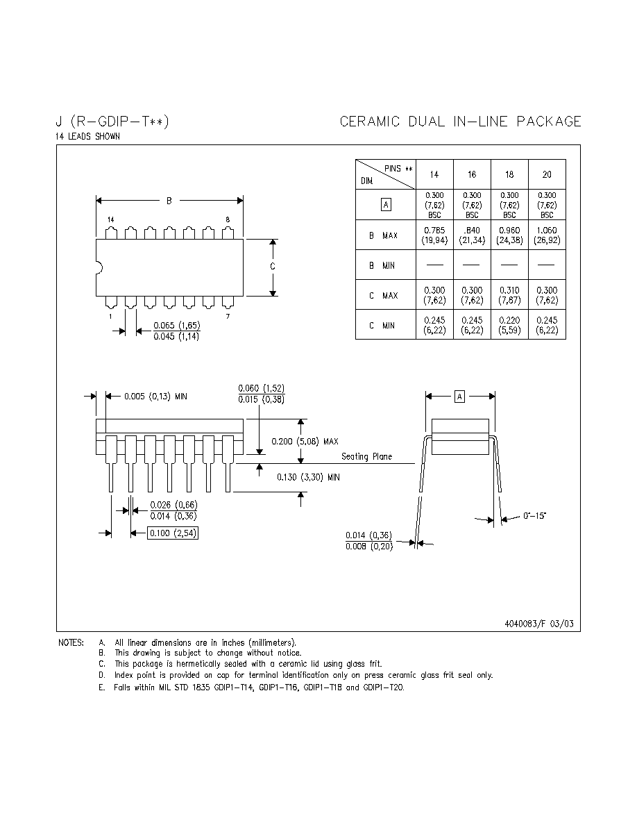
MECHANICAL DATA
MTSS001C ≠ JANUARY 1995 ≠ REVISED FEBRUARY 1999
POST OFFICE BOX 655303
∑
DALLAS, TEXAS 75265
PW (R-PDSO-G**)
PLASTIC SMALL-OUTLINE PACKAGE
14 PINS SHOWN
0,65
M
0,10
0,10
0,25
0,50
0,75
0,15 NOM
Gage Plane
28
9,80
9,60
24
7,90
7,70
20
16
6,60
6,40
4040064/F 01/97
0,30
6,60
6,20
8
0,19
4,30
4,50
7
0,15
14
A
1
1,20 MAX
14
5,10
4,90
8
3,10
2,90
A MAX
A MIN
DIM
PINS **
0,05
4,90
5,10
Seating Plane
0
∞
≠ 8
∞
NOTES: A. All linear dimensions are in millimeters.
B. This drawing is subject to change without notice.
C. Body dimensions do not include mold flash or protrusion not to exceed 0,15.
D. Falls within JEDEC MO-153

IMPORTANT NOTICE
Texas Instruments Incorporated and its subsidiaries (TI) reserve the right to make corrections, modifications,
enhancements, improvements, and other changes to its products and services at any time and to discontinue
any product or service without notice. Customers should obtain the latest relevant information before placing
orders and should verify that such information is current and complete. All products are sold subject to TI's terms
and conditions of sale supplied at the time of order acknowledgment.
TI warrants performance of its hardware products to the specifications applicable at the time of sale in
accordance with TI's standard warranty. Testing and other quality control techniques are used to the extent TI
deems necessary to support this warranty. Except where mandated by government requirements, testing of all
parameters of each product is not necessarily performed.
TI assumes no liability for applications assistance or customer product design. Customers are responsible for
their products and applications using TI components. To minimize the risks associated with customer products
and applications, customers should provide adequate design and operating safeguards.
TI does not warrant or represent that any license, either express or implied, is granted under any TI patent right,
copyright, mask work right, or other TI intellectual property right relating to any combination, machine, or process
in which TI products or services are used. Information published by TI regarding third-party products or services
does not constitute a license from TI to use such products or services or a warranty or endorsement thereof.
Use of such information may require a license from a third party under the patents or other intellectual property
of the third party, or a license from TI under the patents or other intellectual property of TI.
Reproduction of information in TI data books or data sheets is permissible only if reproduction is without
alteration and is accompanied by all associated warranties, conditions, limitations, and notices. Reproduction
of this information with alteration is an unfair and deceptive business practice. TI is not responsible or liable for
such altered documentation.
Resale of TI products or services with statements different from or beyond the parameters stated by TI for that
product or service voids all express and any implied warranties for the associated TI product or service and
is an unfair and deceptive business practice. TI is not responsible or liable for any such statements.
Following are URLs where you can obtain information on other Texas Instruments products and application
solutions:
Products
Applications
Amplifiers
amplifier.ti.com
Audio
www.ti.com/audio
Data Converters
dataconverter.ti.com
Automotive
www.ti.com/automotive
DSP
dsp.ti.com
Broadband
www.ti.com/broadband
Interface
interface.ti.com
Digital Control
www.ti.com/digitalcontrol
Logic
logic.ti.com
Military
www.ti.com/military
Power Mgmt
power.ti.com
Optical Networking
www.ti.com/opticalnetwork
Microcontrollers
microcontroller.ti.com
Security
www.ti.com/security
Telephony
www.ti.com/telephony
Video & Imaging
www.ti.com/video
Wireless
www.ti.com/wireless
Mailing Address:
Texas Instruments
Post Office Box 655303 Dallas, Texas 75265
Copyright
2005, Texas Instruments Incorporated