 | –≠–ª–µ–∫—Ç—Ä–æ–Ω–Ω—ã–π –∫–æ–º–ø–æ–Ω–µ–Ω—Ç: 8408801FA | –°–∫–∞—á–∞—Ç—å:  PDF PDF  ZIP ZIP |
SN54HC112, SN74HC112
DUAL J K NEGATIVE EDGE TRIGGERED FLIP FLOPS
WITH CLEAR AND PRESET
SCLS099F - DECEMBER 1982 - REVISED SEPTEMBER 2003
1
POST OFFICE BOX 655303
∑
DALLAS, TEXAS 75265
D
Wide Operating Voltage Range of 2 V to 6 V
D
Outputs Can Drive Up To 10 LSTTL Loads
D
Low Power Consumption, 40-
µ
A Max I
CC
D
Typical t
pd
= 13 ns
D
±
4-mA Output Drive at 5 V
D
Low Input Current of 1
µ
A Max
description/ordering information
The 'HC112 devices contain two independent J-K
negative-edge-triggered flip-flops. A low level at
the preset (PRE) or clear (CLR) inputs sets or
resets the outputs, regardless of the levels of the
other inputs. When PRE and CLR are inactive
(high), data at the J and K inputs meeting the
setup time requirements are transferred to the
outputs on the negative-going edge of the clock
(CLK) pulse. Clock triggering occurs at a voltage
level and is not directly related to the fall time of the
CLK pulse. Following the hold-time interval, data
at the J and K inputs may be changed without
affecting the levels at the outputs. These versatile
flip-flops perform as toggle flip-flops by tying J and
K high.
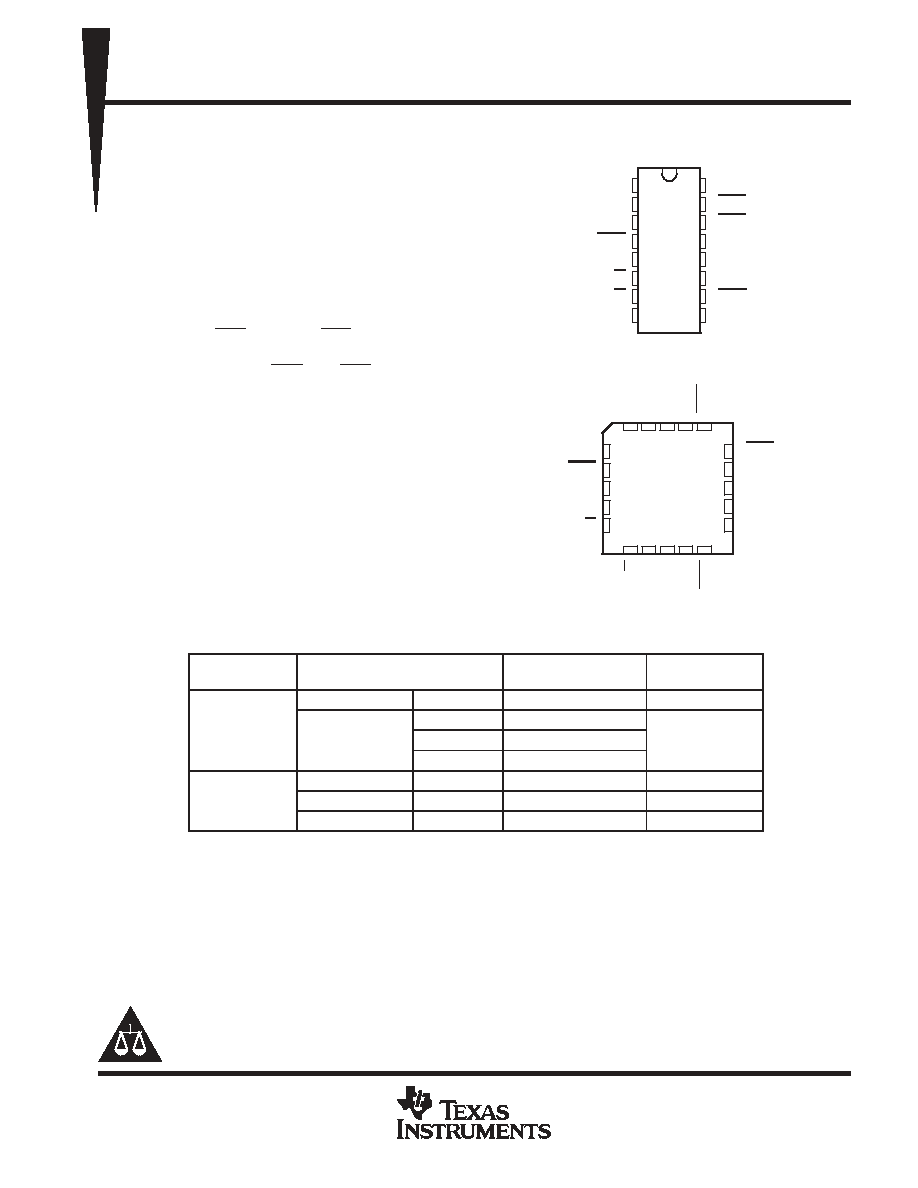
ORDERING INFORMATION
TA
PACKAGE
ORDERABLE
PART NUMBER
TOP-SIDE
MARKING
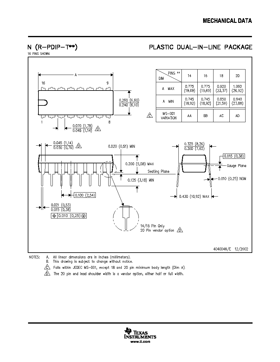
PDIP - N
Tube of 25
SN74HC112N
SN74HC112N
-40
∞
C to 85
∞
C
Tube of 40
SN74HC112D
-40
∞
C to 85
∞
C
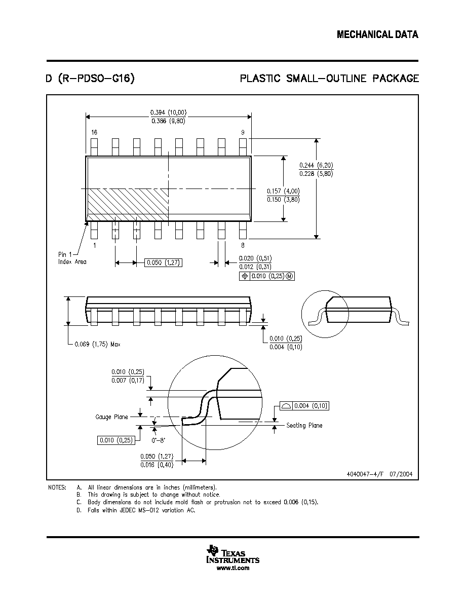
SOIC - D
Reel of 2500
SN74HC112DR
HC112
SOIC - D
Reel of 250
SN74HC112DT
HC112
CDIP - J
Tube of 25
SNJ54HC112J
SNJ54HC112J
-55
∞
C to 125
∞
C
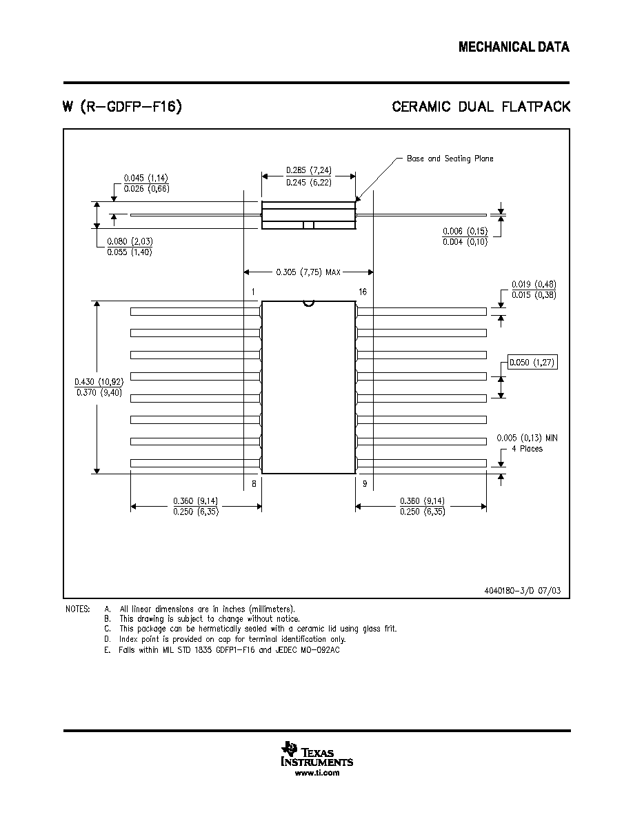
CFP - W
Tube of 150
SNJ54HC112W
SNJ54HC112W
-55 C to 125 C
LCCC - FK
Tube of 55
SNJ54HC112FK
SNJ54HC112FK
Package drawings, standard packing quantities, thermal data, symbolization, and PCB design guidelines are
available at www.ti.com/sc/package.
Please be aware that an important notice concerning availability, standard warranty, and use in critical applications of
Texas Instruments semiconductor products and disclaimers thereto appears at the end of this data sheet.
3
2 1 20 19
9 10 11 12 13
4
5
6
7
8
18
17
16
15
14
2CLR
2CLK
NC
2K
2J
1J
1PRE
NC
1Q
1Q
1K
1CLK
NC
2Q
V
1CLR
2Q
GND
NC
SN54HC112 . . . FK PACKAGE
(TOP VIEW)
CC
NC - No internal connection
1
2
3
4
5
6
7
8
16
15
14
13
12
11
10
9
1CLK
1K
1J
1PRE
1Q
1Q
2Q
GND
V
CC
1CLR
2CLR
2CLK
2K
2J
2PRE
2Q
SN54HC112 . . . J OR W PACKAGE
SN74HC112 . . . D OR N PACKAGE
(TOP VIEW)
2PRE
Copyright
2003, Texas Instruments Incorporated
PRODUCTION DATA information is current as of publication date.
Products conform to specifications per the terms of Texas Instruments
standard warranty. Production processing does not necessarily include
testing of all parameters.
On products compliant to MIL PRF 38535, all parameters are tested
unless otherwise noted. On all other products, production
processing does not necessarily include testing of all parameters.
SN54HC112, SN74HC112
DUAL J K NEGATIVE EDGE TRIGGERED FLIP FLOPS
WITH CLEAR AND PRESET
SCLS099F - DECEMBER 1982 - REVISED SEPTEMBER 2003
2
POST OFFICE BOX 655303
∑
DALLAS, TEXAS 75265
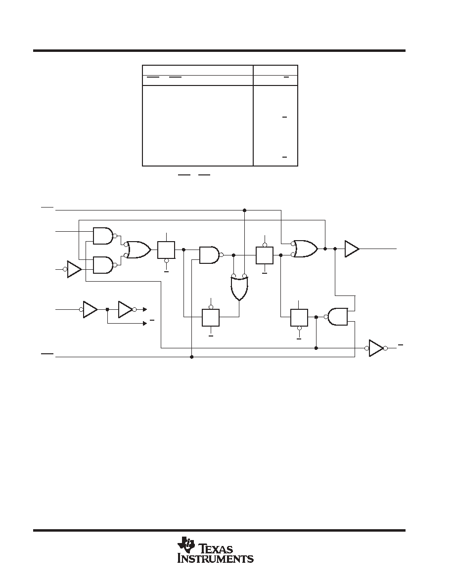
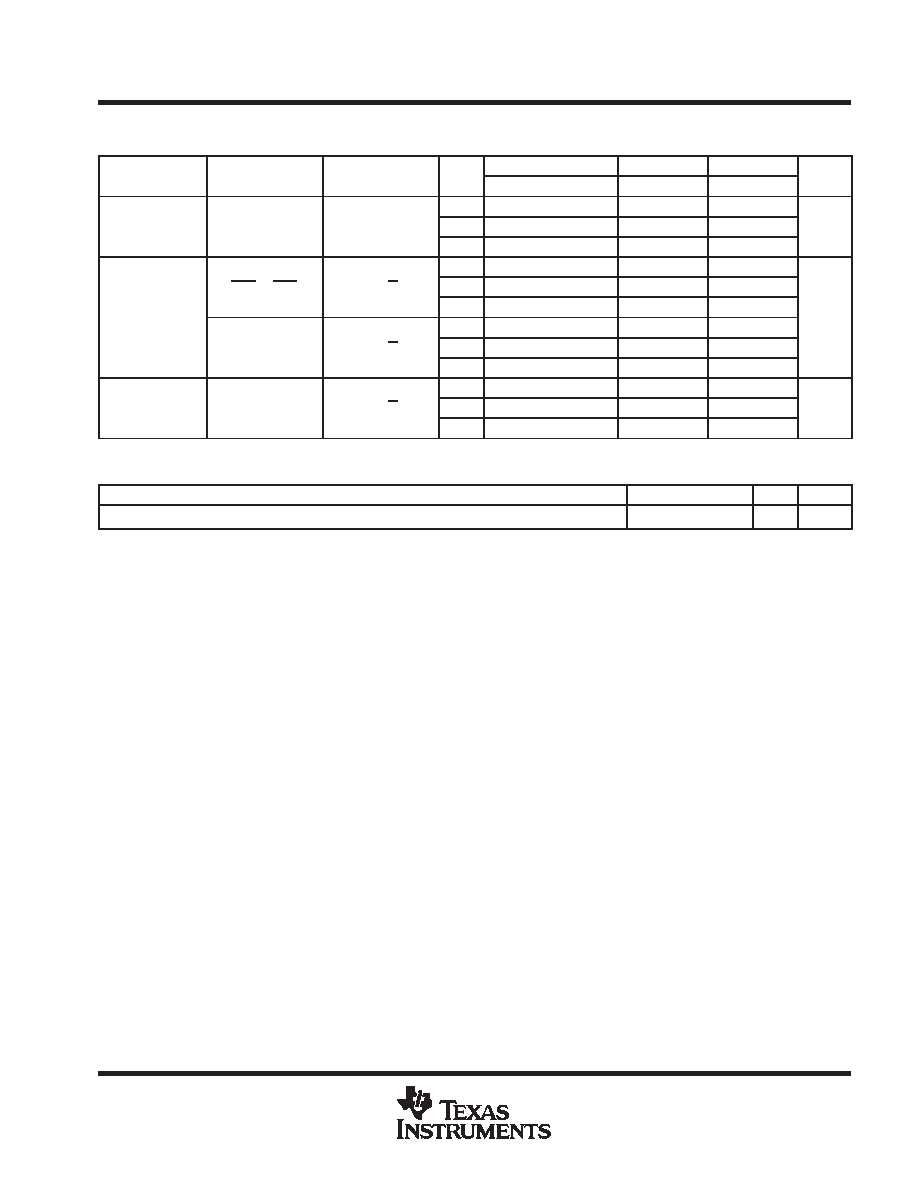
FUNCTION TABLE
INPUTS
OUTPUTS
PRE
CLR
CLK
J
K
Q
Q
L
H
X
X
X
H
L
H
L
X
X
X
L
H
L
L
X
X
X
H
H
H
H
L
L
Q0
Q0
H
H
H
L
H
L
H
H
L
H
L
H
H
H
H
H
Toggle
H
H
H
X
X
Q0
Q0
This configuration is nonstable; that is, it does not persist
when either PRE or CLR returns to its inactive (high) level.
logic diagram, each flip-flop (positive logic)
PRE
CLK
J
CLR
Q
Q
C
C
C
C
K
TG
TG
TG
TG
C
C
C
C
C
C
SN54HC112, SN74HC112
DUAL J K NEGATIVE EDGE TRIGGERED FLIP FLOPS
WITH CLEAR AND PRESET
SCLS099F - DECEMBER 1982 - REVISED SEPTEMBER 2003
3
POST OFFICE BOX 655303
∑
DALLAS, TEXAS 75265
absolute maximum ratings over operating free-air temperature range
Supply voltage range, V
CC
-0.5 V to 7 V
. . . . . . . . . . . . . . . . . . . . . . . . . . . . . . . . . . . . . . . . . . . . . . . . . . . . . . . . . .
Input clamp current, I
IK
(V
I
< 0 or V
I
> V
CC
) (see Note 1)
±
20 mA
. . . . . . . . . . . . . . . . . . . . . . . . . . . . . . . . . . . .
Output clamp current, I
OK
(V
O
< 0 or V
O
> V
CC
) (see Note 1)
±
20 mA
. . . . . . . . . . . . . . . . . . . . . . . . . . . . . . . .
Continuous output current, I
O
(V
O
= 0 to V
CC
)
±
25 mA
. . . . . . . . . . . . . . . . . . . . . . . . . . . . . . . . . . . . . . . . . . . . . .
Continuous current through V
CC
or GND
±
50 mA
. . . . . . . . . . . . . . . . . . . . . . . . . . . . . . . . . . . . . . . . . . . . . . . . . . .
Package thermal impedance,
JA
(see Note 2): D package
73
∞
C/W
. . . . . . . . . . . . . . . . . . . . . . . . . . . . . . . . . . .
N package
67
∞
C/W
. . . . . . . . . . . . . . . . . . . . . . . . . . . . . . . . . . .
Storage temperature range, T
stg
-65
∞
C to 150
∞
C
. . . . . . . . . . . . . . . . . . . . . . . . . . . . . . . . . . . . . . . . . . . . . . . . . . .
Stresses beyond those listed under "absolute maximum ratings" may cause permanent damage to the device. These are stress ratings only, and
functional operation of the device at these or any other conditions beyond those indicated under "recommended operating conditions" is not
implied. Exposure to absolute-maximum-rated conditions for extended periods may affect device reliability.
NOTES:
1. The input and output voltage ratings may be exceeded if the input and output current ratings are observed.
2. The package thermal impedance is calculated in accordance with JESD 51-7.
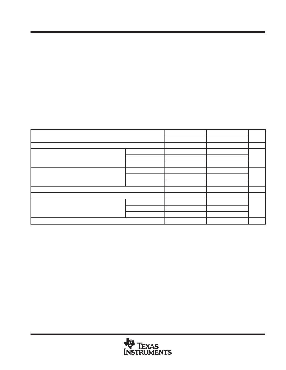
recommended operating conditions (see Note 3)
SN54HC112
SN74HC112
UNIT
MIN
NOM
MAX
MIN
NOM
MAX
UNIT
VCC
Supply voltage
2
5
6
2
5
6
V
VCC = 2 V
1.5
1.5
VIH
High-level input voltage
VCC = 4.5 V
3.15
3.15
V
VIH
High-level input voltage
VCC = 6 V
4.2
4.2
V
VCC = 2 V
0.5
0.5
VIL
Low-level input voltage
VCC = 4.5 V
1.35
1.35
V
VIL
Low-level input voltage
VCC = 6 V
1.8
1.8
V
VI
Input voltage
0
VCC
0
VCC
V
VO
Output voltage
0
VCC
0
VCC
V
VCC = 2 V
1000
1000
tt
Input transition (rise and fall) time
VCC = 4.5 V
500
500
ns
tt
Input transition (rise and fall) time
VCC = 6 V
400
400
ns
TA
Operating free-air temperature
-55
125
-40
85
∞
C
If this device is used in the threshold region (from VILmax = 0.5 V to VIHmin = 1.5 V), there is a potential to go into the wrong state from induced
grounding, causing double clocking. Operating with the inputs at tt = 1000 ns and VCC = 2 V does not damage the device; however, functionally,
the CLK inputs are not ensured while in the shift, count, or toggle operating modes.
NOTE 3: All unused inputs of the device must be held at VCC or GND to ensure proper device operation. Refer to the TI application report,
Implications of Slow or Floating CMOS Inputs, literature number SCBA004.
SN54HC112, SN74HC112
DUAL J K NEGATIVE EDGE TRIGGERED FLIP FLOPS
WITH CLEAR AND PRESET
SCLS099F - DECEMBER 1982 - REVISED SEPTEMBER 2003
4
POST OFFICE BOX 655303
∑
DALLAS, TEXAS 75265
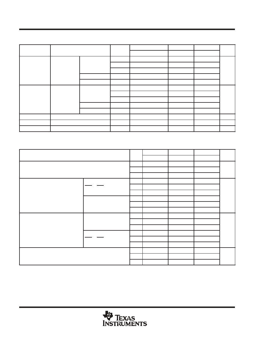
electrical characteristics over recommended operating free-air temperature range (unless
otherwise noted)
PARAMETER
TEST CONDITIONS
VCC
TA = 25
∞
C
SN54HC112
SN74HC112
UNIT
PARAMETER
TEST CONDITIONS
VCC
MIN
TYP
MAX
MIN
MAX
MIN
MAX
UNIT
2 V
1.9
1.998
1.9
1.9
IOH = -20
µ
A
4.5 V
4.4
4.499
4.4
4.4
VOH
VI = VIH or VIL
IOH = -20
µ
A
6 V
5.9
5.999
5.9
5.9
V
VOH
VI = VIH or VIL
IOH = -4 mA
4.5 V
3.98
4.3
3.7
3.84
V
IOH = -5.2 mA
6 V
5.48
5.8
5.2
5.34
2 V
0.002
0.1
0.1
0.1
IOL = 20
µ
A
4.5 V
0.001
0.1
0.1
0.1
VOL
VI = VIH or VIL
IOL = 20
µ
A
6 V
0.001
0.1
0.1
0.1
V
VOL
VI = VIH or VIL
IOL = 4 mA
4.5 V
0.17
0.26
0.4
0.33
V
IOL = 5.2 mA
6 V
0.15
0.26
0.4
0.33
II
VI = VCC or 0
6 V
±
0.1
±
100
±
1000
±
1000
nA
ICC
VI = VCC or 0,
IO = 0
6 V
4
80
40
µ
A
Ci
2 V to 6 V
3
10
10
10
pF
timing requirements over recommended operating free-air temperature range (unless otherwise
noted)
VCC
TA = 25
∞
C
SN54HC112
SN74HC112
UNIT
VCC
MIN
MAX
MIN
MAX
MIN
MAX
UNIT
2 V
5
3.4
4
fclock
Clock frequency
4.5 V
25
17
20
MHz
fclock
Clock frequency
6 V
29
20
24
MHz
2 V
100
150
125
PRE or CLR low
4.5 V
20
30
25
tw
Pulse duration
PRE or CLR low
6 V
17
25
21
ns
tw
Pulse duration
2 V
100
150
125
ns
CLK high or low
4.5 V
20
30
25
CLK high or low
6 V
17
25
21
2 V
100
150
125
Data (J, K)
4.5 V
20
30
25
tsu
Setup time before CLK
Data (J, K)
6 V
17
25
21
ns
tsu
Setup time before CLK
2 V
100
150
125
ns
PRE or CLR inactive
4.5 V
20
30
25
PRE or CLR inactive
6 V
17
25
21
2 V
0
0
0
th
Hold time, data after CLK
4.5 V
0
0
0
ns
th
Hold time, data after CLK
6 V
0
0
0
ns
SN54HC112, SN74HC112
DUAL J K NEGATIVE EDGE TRIGGERED FLIP FLOPS
WITH CLEAR AND PRESET
SCLS099F - DECEMBER 1982 - REVISED SEPTEMBER 2003
5
POST OFFICE BOX 655303
∑
DALLAS, TEXAS 75265
switching characteristics over recommended operating free-air temperature range, C
L
= 50 pF
(unless otherwise noted) (see Figure 1)
PARAMETER
FROM
TO
VCC
TA = 25
∞
C
SN54HC112
SN74HC112
UNIT
PARAMETER
FROM
(INPUT)
TO
(OUTPUT)
VCC
MIN
TYP
MAX
MIN
MAX
MIN
MAX
UNIT
2 V
5
10
3.4
4
fmax
4.5 V
25
50
17
20
MHz
fmax
6 V
29
60
20
24
MHz
2 V
54
165
245
205
PRE or CLR
Q or Q
4.5 V
16
33
49
41
tpd
PRE or CLR
Q or Q
6 V
13
28
42
35
ns
tpd
2 V
56
125
185
155
ns
CLK
Q or Q
4.5 V
16
25
37
31
CLK
Q or Q
6 V
13
21
31
26
2 V
29
75
110
95
tt
Q or Q
4.5 V
9
15
22
19
ns
tt
Q or Q
6 V
8
13
19
16
ns
operating characteristics, T
A
= 25
∞
C
PARAMETER
TEST CONDITIONS
TYP
UNIT
Cpd
Power dissipation capacitance
No load
35
pF
SN54HC112, SN74HC112
DUAL J K NEGATIVE EDGE TRIGGERED FLIP FLOPS
WITH CLEAR AND PRESET
SCLS099F - DECEMBER 1982 - REVISED SEPTEMBER 2003
6
POST OFFICE BOX 655303
∑
DALLAS, TEXAS 75265
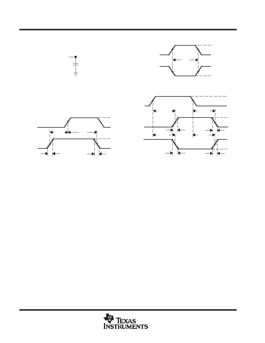
PARAMETER MEASUREMENT INFORMATION
VOLTAGE WAVEFORMS
SETUP AND HOLD AND INPUT RISE AND FALL TIMES
VOLTAGE WAVEFORMS
PULSE DURATIONS
th
tsu
50%
50%
50%
10%
10%
90%
90%
VCC
VCC
0 V
0 V
tr
tf
Reference
Input
Data
Input
50%
High-Level
Pulse
50%
VCC
0 V
50%
50%
VCC
0 V
tw
Low-Level
Pulse
VOLTAGE WAVEFORMS
PROPAGATION DELAY AND OUTPUT TRANSITION TIMES
50%
50%
50%
10%
10%
90%
90%
VCC
VOH
VOL
0 V
tr
tf
Input
In-Phase
Output
50%
tPLH
tPHL
50%
50%
10%
10%
90%
90%
VOH
VOL
tr
tf
tPHL
tPLH
Out-of-Phase
Output
NOTES: A. CL includes probe and test-fixture capacitance.
B. Phase relationships between waveforms were chosen arbitrarily. All input pulses are supplied by generators having the following
characteristics: PRR
1 MHz, ZO = 50
, tr = 6 ns, tf = 6 ns.
C. For clock inputs, fmax is measured when the input duty cycle is 50%.
D. The outputs are measured one at a time with one input transition per measurement.
E. tPLH and tPHL are the same as tpd.
Test
Point
From Output
Under Test
CL = 50 pF
(see Note A)
LOAD CIRCUIT
Figure 1. Load Circuit and Voltage Waveforms
PACKAGING INFORMATION
Orderable Device
Status
(1)
Package
Type
Package
Drawing
Pins Package
Qty
Eco Plan
(2)
Lead/Ball Finish
MSL Peak Temp
(3)
84088012A
ACTIVE
LCCC
FK
20
1
None
Call TI
Level-NC-NC-NC
8408801EA
ACTIVE
CDIP
J
16
1
None
Call TI
Level-NC-NC-NC
8408801FA
ACTIVE
CFP
W
16
1
None
Call TI
Level-NC-NC-NC
JM38510/65305BEA
ACTIVE
CDIP
J
16
1
None
Call TI
Level-NC-NC-NC
SN54HC112J
ACTIVE
CDIP
J
16
1
None
Call TI
Level-NC-NC-NC
SN74HC112D
ACTIVE
SOIC
D
16
40
Pb-Free
(RoHS)
CU NIPDAU
Level-2-260C-1 YEAR/
Level-1-235C-UNLIM
SN74HC112DR
ACTIVE
SOIC
D
16
2500
Pb-Free
(RoHS)
CU NIPDAU
Level-2-260C-1 YEAR/
Level-1-235C-UNLIM
SN74HC112DT
ACTIVE
SOIC
D
16
250
Pb-Free
(RoHS)
CU NIPDAU
Level-2-260C-1 YEAR/
Level-1-235C-UNLIM
SN74HC112N
ACTIVE
PDIP
N
16
25
Pb-Free
(RoHS)
CU NIPDAU
Level-NC-NC-NC
SN74HC112N3
OBSOLETE
PDIP
N
16
None
Call TI
Call TI
SNJ54HC112FK
ACTIVE
LCCC
FK
20
1
None
Call TI
Level-NC-NC-NC
SNJ54HC112J
ACTIVE
CDIP
J
16
1
None
Call TI
Level-NC-NC-NC
SNJ54HC112W
ACTIVE
CFP
W
16
1
None
Call TI
Level-NC-NC-NC
(1)
The marketing status values are defined as follows:
ACTIVE: Product device recommended for new designs.
LIFEBUY: TI has announced that the device will be discontinued, and a lifetime-buy period is in effect.
NRND: Not recommended for new designs. Device is in production to support existing customers, but TI does not recommend using this part in
a new design.
PREVIEW: Device has been announced but is not in production. Samples may or may not be available.
OBSOLETE: TI has discontinued the production of the device.
(2)
Eco Plan - May not be currently available - please check
http://www.ti.com/productcontent
for the latest availability information and additional
product content details.
None: Not yet available Lead (Pb-Free).
Pb-Free (RoHS): TI's terms "Lead-Free" or "Pb-Free" mean semiconductor products that are compatible with the current RoHS requirements
for all 6 substances, including the requirement that lead not exceed 0.1% by weight in homogeneous materials. Where designed to be soldered
at high temperatures, TI Pb-Free products are suitable for use in specified lead-free processes.
Green (RoHS & no Sb/Br): TI defines "Green" to mean "Pb-Free" and in addition, uses package materials that do not contain halogens,
including bromine (Br) or antimony (Sb) above 0.1% of total product weight.
(3)
MSL, Peak Temp. -- The Moisture Sensitivity Level rating according to the JEDECindustry standard classifications, and peak solder
temperature.
Important Information and Disclaimer:The information provided on this page represents TI's knowledge and belief as of the date that it is
provided. TI bases its knowledge and belief on information provided by third parties, and makes no representation or warranty as to the
accuracy of such information. Efforts are underway to better integrate information from third parties. TI has taken and continues to take
reasonable steps to provide representative and accurate information but may not have conducted destructive testing or chemical analysis on
incoming materials and chemicals. TI and TI suppliers consider certain information to be proprietary, and thus CAS numbers and other limited
information may not be available for release.
In no event shall TI's liability arising out of such information exceed the total purchase price of the TI part(s) at issue in this document sold by TI
to Customer on an annual basis.
PACKAGE OPTION ADDENDUM
www.ti.com
28-Feb-2005
Addendum-Page 1
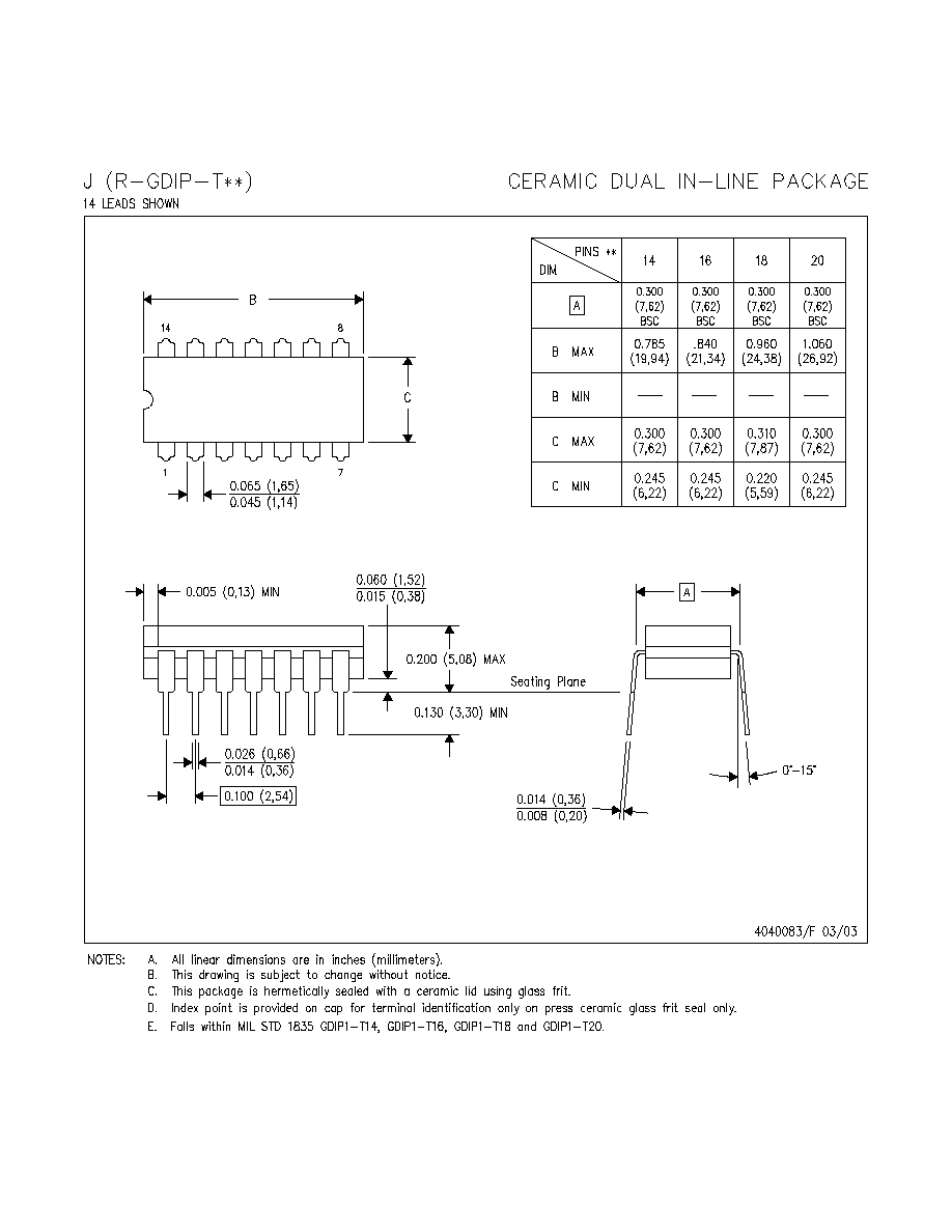
MECHANICAL DATA
MLCC006B ≠ OCTOBER 1996
POST OFFICE BOX 655303
∑
DALLAS, TEXAS 75265
FK (S-CQCC-N**)
LEADLESS CERAMIC CHIP CARRIER
4040140 / D 10/96
28 TERMINAL SHOWN
B
0.358
(9,09)
MAX
(11,63)
0.560
(14,22)
0.560
0.458
0.858
(21,8)
1.063
(27,0)
(14,22)
A
NO. OF
MIN
MAX
0.358
0.660
0.761
0.458
0.342
(8,69)
MIN
(11,23)
(16,26)
0.640
0.739
0.442
(9,09)
(11,63)
(16,76)
0.962
1.165
(23,83)
0.938
(28,99)
1.141
(24,43)
(29,59)
(19,32)
(18,78)
**
20
28
52
44
68
84
0.020 (0,51)
TERMINALS
0.080 (2,03)
0.064 (1,63)
(7,80)
0.307
(10,31)
0.406
(12,58)
0.495
(12,58)
0.495
(21,6)
0.850
(26,6)
1.047
0.045 (1,14)
0.045 (1,14)
0.035 (0,89)
0.035 (0,89)
0.010 (0,25)
12
13
14
15
16
18
17
11
10
8
9
7
5
4
3
2
0.020 (0,51)
0.010 (0,25)
6
1
28
26
27
19
21
B SQ
A SQ
22
23
24
25
20
0.055 (1,40)
0.045 (1,14)
0.028 (0,71)
0.022 (0,54)
0.050 (1,27)
NOTES: A. All linear dimensions are in inches (millimeters).
B. This drawing is subject to change without notice.
C. This package can be hermetically sealed with a metal lid.
D. The terminals are gold plated.
E. Falls within JEDEC MS-004

IMPORTANT NOTICE
Texas Instruments Incorporated and its subsidiaries (TI) reserve the right to make corrections, modifications,
enhancements, improvements, and other changes to its products and services at any time and to discontinue
any product or service without notice. Customers should obtain the latest relevant information before placing
orders and should verify that such information is current and complete. All products are sold subject to TI's terms
and conditions of sale supplied at the time of order acknowledgment.
TI warrants performance of its hardware products to the specifications applicable at the time of sale in
accordance with TI's standard warranty. Testing and other quality control techniques are used to the extent TI
deems necessary to support this warranty. Except where mandated by government requirements, testing of all
parameters of each product is not necessarily performed.
TI assumes no liability for applications assistance or customer product design. Customers are responsible for
their products and applications using TI components. To minimize the risks associated with customer products
and applications, customers should provide adequate design and operating safeguards.
TI does not warrant or represent that any license, either express or implied, is granted under any TI patent right,
copyright, mask work right, or other TI intellectual property right relating to any combination, machine, or process
in which TI products or services are used. Information published by TI regarding third-party products or services
does not constitute a license from TI to use such products or services or a warranty or endorsement thereof.
Use of such information may require a license from a third party under the patents or other intellectual property
of the third party, or a license from TI under the patents or other intellectual property of TI.
Reproduction of information in TI data books or data sheets is permissible only if reproduction is without
alteration and is accompanied by all associated warranties, conditions, limitations, and notices. Reproduction
of this information with alteration is an unfair and deceptive business practice. TI is not responsible or liable for
such altered documentation.
Resale of TI products or services with statements different from or beyond the parameters stated by TI for that
product or service voids all express and any implied warranties for the associated TI product or service and
is an unfair and deceptive business practice. TI is not responsible or liable for any such statements.
Following are URLs where you can obtain information on other Texas Instruments products and application
solutions:
Products
Applications
Amplifiers
amplifier.ti.com
Audio
www.ti.com/audio
Data Converters
dataconverter.ti.com
Automotive
www.ti.com/automotive
DSP
dsp.ti.com
Broadband
www.ti.com/broadband
Interface
interface.ti.com
Digital Control
www.ti.com/digitalcontrol
Logic
logic.ti.com
Military
www.ti.com/military
Power Mgmt
power.ti.com
Optical Networking
www.ti.com/opticalnetwork
Microcontrollers
microcontroller.ti.com
Security
www.ti.com/security
Telephony
www.ti.com/telephony
Video & Imaging
www.ti.com/video
Wireless
www.ti.com/wireless
Mailing Address:
Texas Instruments
Post Office Box 655303 Dallas, Texas 75265
Copyright
2005, Texas Instruments Incorporated