 | –≠–ª–µ–∫—Ç—Ä–æ–Ω–Ω—ã–π –∫–æ–º–ø–æ–Ω–µ–Ω—Ç: 84145012A | –°–∫–∞—á–∞—Ç—å:  PDF PDF  ZIP ZIP |
SN54ALS832A, SN54AS832B, SN74ALS832A, SN74AS832B
HEX 2-INPUT OR DRIVERS
SDAS017C ≠ DECEMBER 1982 ≠ REVISED JANUARY 1995
Copyright
©
1995, Texas Instruments Incorporated
1
POST OFFICE BOX 655303
∑
DALLAS, TEXAS 75265
∑
High Capacitive-Drive Capability
∑
ALS832A Has Typical Delay Time of 4.8 ns
(C
L
= 50 pF) and Typical Power Dissipation
of 4.5 mW Per Gate
∑
AS832B Has Typical Delay Time of 3.2 ns
(C
L
= 50 pF) and Typical Power Dissipation
of Less Than 13 mW Per Gate
∑
Package Options Include Plastic
Small-Outline (DW) Packages, Ceramic
Chip Carriers (FK), and Standard Plastic (N)
and Ceramic (J) 300-mil DIPs
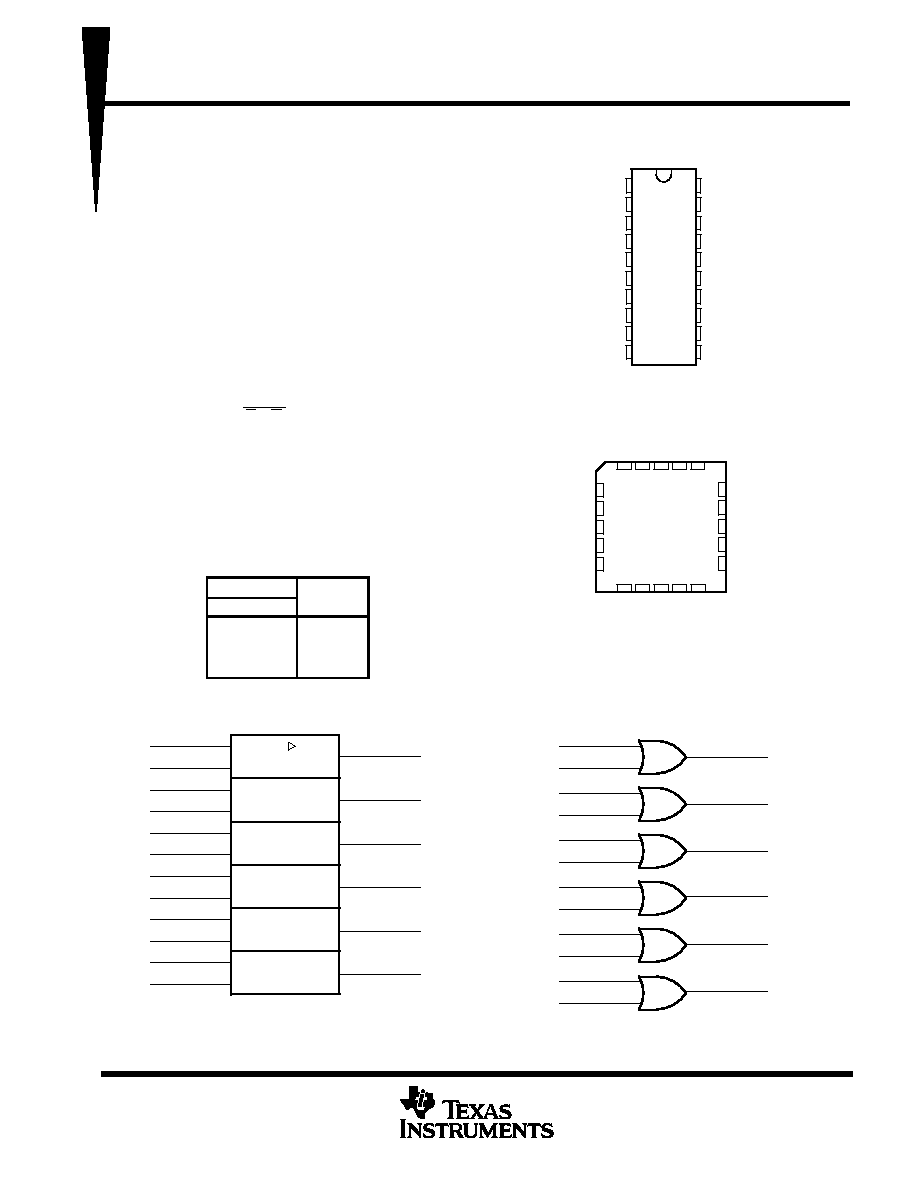
description
These devices contain six independent 2-input
OR drivers. They perform the Boolean functions
Y = A + B or Y = A
∑
B in positive logic.
The SN54ALS832A and SN54AS832B are
characterized for operation over the full military
temperature range of ≠ 55
∞
C to 125
∞
C. The
SN74ALS832A and SN74AS832B are
characterized for operation from 0
∞
C to 70
∞
C.
FUNCTION TABLE
(each driver)
INPUTS
OUTPUT
A
B
Y
H
X
H
X
H
H
L
L
L
logic symbol
logic diagram (positive logic)
1
1A
2
1B
4
2A
5
2B
7
3A
8
3B
12
4A
13
4B
1Y
3
2Y
6
3Y
9
4Y
11
15
5A
16
5B
18
6A
19
6B
5Y
14
6Y
17
1Y
3
1
1A
2
1B
2Y
6
4
2A
5
2B
3Y
9
7
3A
8
3B
4Y
11
12
4A
13
4B
5Y
14
15
5A
16
5B
6Y
17
18
6A
19
6B
1
This symbol is in accordance with ANSI/IEEE Std 91-1984 and
IEC Publication 617-12.
1
2
3
4
5
6
7
8
9
10
20
19
18
17
16
15
14
13
12
11
1A
1B
1Y
2A
2B
2Y
3A
3B
3Y
GND
V
CC
6B
6A
6Y
5B
5A
5Y
4B
4A
4Y
SN54ALS832A, SN54AS832B . . . J PACKAGE
SN74ALS832A, SN74AS832B . . . DW OR N PACKAGE
(TOP VIEW)
3
2
1 20 19
9 10 11 12 13
4
5
6
7
8
18
17
16
15
14
6A
6Y
5B
5A
5Y
2A
2B
2Y
3A
3B
SN54ALS832A, SN54AS832B . . . FK PACKAGE
(TOP VIEW)
1Y
1B
1A
4A
4B
6B
3Y
GND
4Y
V
CC
PRODUCTION DATA information is current as of publication date.
Products conform to specifications per the terms of Texas Instruments
standard warranty. Production processing does not necessarily include
testing of all parameters.
SN54ALS832A, SN54AS832B, SN74ALS832A, SN74AS832B
HEX 2-INPUT OR DRIVERS
SDAS017C ≠ DECEMBER 1982 ≠ REVISED JANUARY 1995
2
POST OFFICE BOX 655303
∑
DALLAS, TEXAS 75265
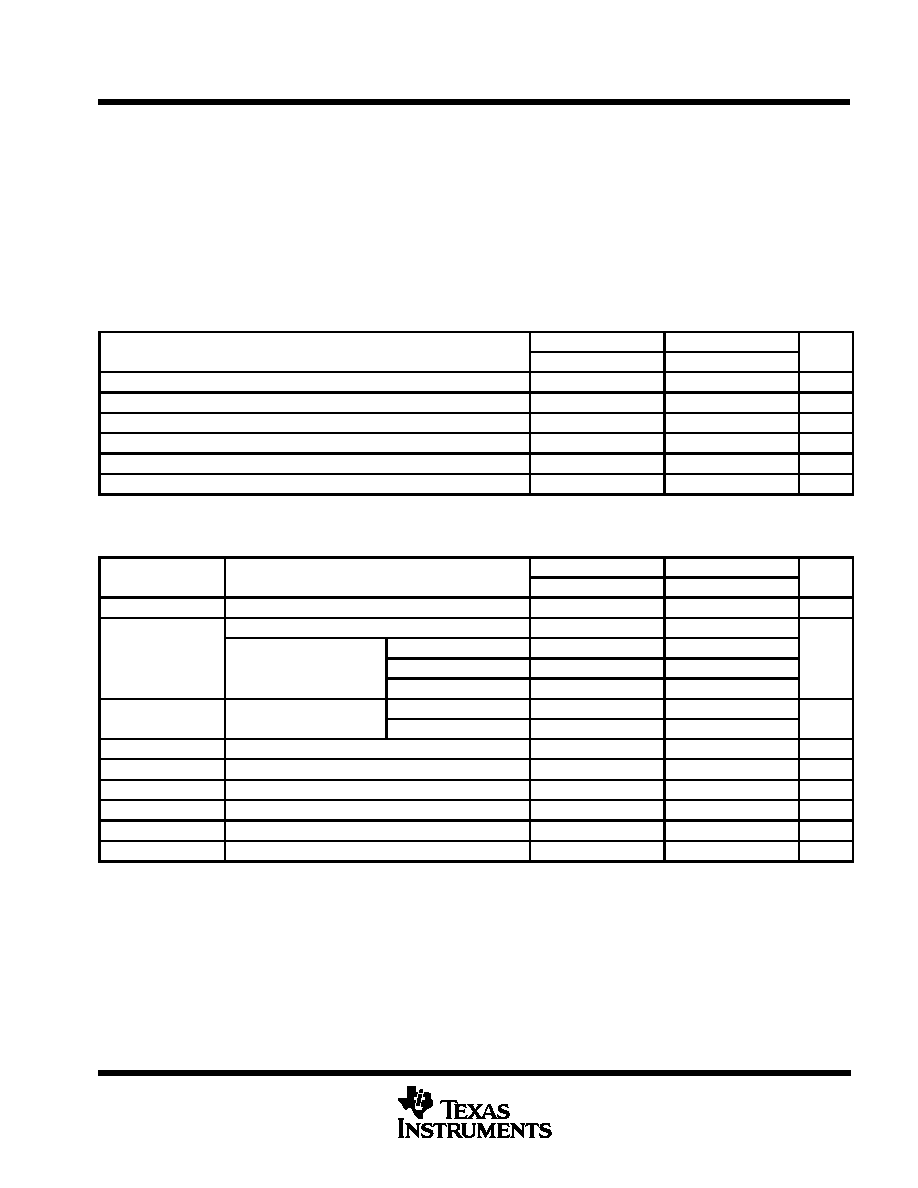
absolute maximum ratings over operating free-air temperature range (unless otherwise noted)
Supply voltage, V
CC
7 V
. . . . . . . . . . . . . . . . . . . . . . . . . . . . . . . . . . . . . . . . . . . . . . . . . . . . . . . . . . . . . . . . . . . . . . . .
Input voltage, V
I
7 V
. . . . . . . . . . . . . . . . . . . . . . . . . . . . . . . . . . . . . . . . . . . . . . . . . . . . . . . . . . . . . . . . . . . . . . . . . . . .
Operating free-air temperature range, T
A
: SN54ALS832A
≠ 55
∞
C to 125
∞
C
. . . . . . . . . . . . . . . . . . . . . . . . . . .
SN74ALS832A
0
∞
C to 70
∞
C
. . . . . . . . . . . . . . . . . . . . . . . . . . . . . . .
Storage temperature range
≠ 65
∞
C to 150
∞
C
. . . . . . . . . . . . . . . . . . . . . . . . . . . . . . . . . . . . . . . . . . . . . . . . . . . . . . .
Stresses beyond those listed under "absolute maximum ratings" may cause permanent damage to the device. These are stress ratings only, and
functional operation of the device at these or any other conditions beyond those indicated under "recommended operating conditions" is not
implied. Exposure to absolute-maximum-rated conditions for extended periods may affect device reliability.
recommended operating conditions
SN54ALS832A
SN74ALS832A
UNIT
MIN
NOM
MAX
MIN
NOM
MAX
UNIT
VCC
Supply voltage
4.5
5
5.5
4.5
5
5.5
V
VIH
High-level input voltage
2
2
V
VIL
Low-level input voltage
0.7
0.8
V
IOH
High-level output current
≠ 12
≠ 15
mA
IOL
Low-level output current
12
24
mA
TA
Operating free-air temperature
≠ 55
125
0
70
∞
C
electrical characteristics over recommended operating free-air temperature range (unless
otherwise noted)
PARAMETER
TEST CONDITIONS
SN54ALS832A
SN74ALS832A
UNIT
PARAMETER
TEST CONDITIONS
MIN
TYP
MAX
MIN
TYP
MAX
UNIT
VIK
VCC = 4.5 V,
II = ≠18 mA
≠1.5
≠1.5
V
VCC = 4.5 V to 5.5 V,
IOH = ≠ 0.4 mA
VCC ≠ 2
VCC ≠ 2
VOH
IOH = ≠ 3 mA
2.4
3.2
2.4
3.2
V
VOH
VCC = 4.5 V
IOH = ≠ 12 mA
2
V
IOH = ≠ 15 mA
2
VOL
VCC = 4 5 V
IOL = 12 mA
0.25
0.4
0.25
0.4
V
VOL
VCC = 4.5 V
IOL = 24 mA
0.35
0.5
V
II
VCC = 5.5 V,
VI = 7 V
0.1
0.1
mA
IIH
VCC = 5.5 V,
VI = 2.7 V
20
20
µ
A
IIL
VCC = 5.5 V,
VI = 0.4 V
≠ 0.1
≠ 0.1
mA
IOß
VCC = 5.5 V,
VO = 2.25 V
≠ 20
≠ 112
≠ 30
≠ 112
mA
ICCH
VCC = 5.5 V,
VI = 4.5 V
6
9
6
9
mA
ICCL
VCC = 5.5 V,
VI = 0
9.5
16
9.5
16
mA
All typical values are at VCC = 5 V, TA = 25
∞
C.
ß The output conditions have been chosen to produce a current that closely approximates one half of the true short-circuit output current, IOS.

SN54ALS832A, SN54AS832B, SN74ALS832A, SN74AS832B
HEX 2-INPUT OR DRIVERS
SDAS017C ≠ DECEMBER 1982 ≠ REVISED JANUARY 1995
3
POST OFFICE BOX 655303
∑
DALLAS, TEXAS 75265
switching characteristics (see Figure 1)
PARAMETER
FROM
(INPUT)
TO
(OUTPUT)
VCC = 4.5 V to 5.5 V,
CL = 50 pF,
RL = 500
,
TA = MIN to MAX
UNIT
(INPUT)
(OUTPUT)
SN54ALS832A
SN74ALS832A
MIN
MAX
MIN
MAX
tPLH
A or B
Y
1
13
2
9
ns
tPHL
A or B
Y
1
11
1
8
ns
For conditions shown as MIN or MAX, use the appropriate value specified under recommended operating conditions.
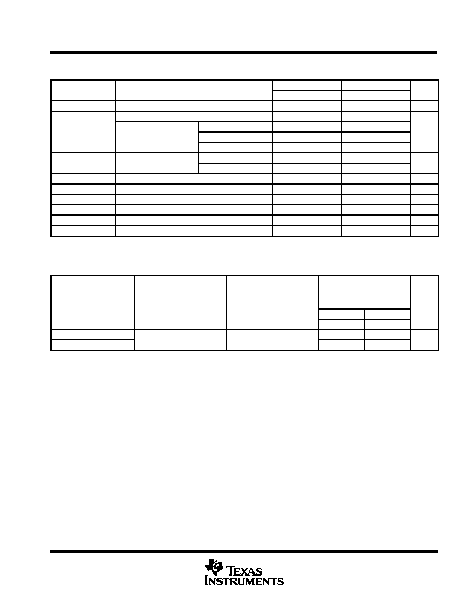
absolute maximum ratings over operating free-air temperature range (unless otherwise noted)
Supply voltage, V
CC
7 V
. . . . . . . . . . . . . . . . . . . . . . . . . . . . . . . . . . . . . . . . . . . . . . . . . . . . . . . . . . . . . . . . . . . . . . . .
Input voltage, V
I
7 V
. . . . . . . . . . . . . . . . . . . . . . . . . . . . . . . . . . . . . . . . . . . . . . . . . . . . . . . . . . . . . . . . . . . . . . . . . . . .
Operating free-air temperature range, T
A
: SN54AS832B
≠ 55
∞
C to 125
∞
C
. . . . . . . . . . . . . . . . . . . . . . . . . . . . .
SN74AS832B
0
∞
C to 70
∞
C
. . . . . . . . . . . . . . . . . . . . . . . . . . . . . . . . .
Storage temperature range
≠ 65
∞
C to 150
∞
C
. . . . . . . . . . . . . . . . . . . . . . . . . . . . . . . . . . . . . . . . . . . . . . . . . . . . . . .
Stresses beyond those listed under "absolute maximum ratings" may cause permanent damage to the device. These are stress ratings only, and
functional operation of the device at these or any other conditions beyond those indicated under "recommended operating conditions" is not
implied. Exposure to absolute-maximum-rated conditions for extended periods may affect device reliability.
recommended operating conditions
ß
SN54AS832B
SN74AS832B
UNIT
MIN
NOM
MAX
MIN
NOM
MAX
UNIT
VCC
Supply voltage
4.5
5
5.5
4.5
5
5.5
V
VIH
High-level input voltage
2
2
V
VIL
Low-level input voltage
0.8
0.8
V
IOH
High-level output current
≠ 40
≠ 48
mA
IOL
Low-level output current
40
48
mA
TA
Operating free-air temperature
≠ 55
125
0
70
∞
C
ß These high sink- or source-current devices are not recommended for use above 40 MHz.
SN54ALS832A, SN54AS832B, SN74ALS832A, SN74AS832B
HEX 2-INPUT OR DRIVERS
SDAS017C ≠ DECEMBER 1982 ≠ REVISED JANUARY 1995
4
POST OFFICE BOX 655303
∑
DALLAS, TEXAS 75265
electrical characteristics over recommended operating free-air temperature range (unless
otherwise noted)
PARAMETER
TEST CONDITIONS
SN54AS832B
SN74AS832B
UNIT
PARAMETER
TEST CONDITIONS
MIN
TYP
MAX
MIN
TYP
MAX
UNIT
VIK
VCC = 4.5 V,
II = ≠18 mA
≠1.2
≠1.2
V
VCC = 4.5 V to 5.5 V,
IOH = ≠ 2 mA
VCC ≠ 2
VCC ≠ 2
VOH
IOH = ≠ 3 mA
2.4
3.2
2.4
3.2
V
VOH
VCC = 4.5 V
IOH = ≠ 40 mA
2
V
IOH = ≠ 48 mA
2
VOL
VCC = 4 5 V
IOL = 40 mA
0.25
0.5
V
VOL
VCC = 4.5 V
IOL = 48 mA
0.35
0.5
V
II
VCC = 5.5 V,
VI = 7 V
0.1
0.1
mA
IIH
VCC = 5.5 V,
VI = 2.7 V
20
20
µ
A
IIL
VCC = 5.5 V,
VI = 0.4 V
≠ 0.5
≠ 0.5
mA
IO
VCC = 5.5 V,
VO = 2.25 V
≠ 50
≠ 200
≠ 50
≠ 200
mA
ICCH
VCC = 5.5 V,
VI = 4.5 V
11
17
11
17
mA
ICCL
VCC = 5.5 V,
VI = 0
22
36
22
36
mA
All typical values are at VCC = 5 V, TA = 25
∞
C.
The output conditions have been chosen to produce a current that closely approximates one half of the true short-circuit output current, IOS.
switching characteristics (see Figure 1)
PARAMETER
FROM
(INPUT)
TO
(OUTPUT)
VCC = 4.5 V to 5.5 V,
CL = 50 pF,
RL = 500
,
TA = MIN to MAXß
UNIT
(INPUT)
(OUTPUT)
SN54AS832B
SN74AS832B
MIN
MAX
MIN
MAX
tPLH
A or B
Y
1
7.5
1
6.3
ns
tPHL
A or B
Y
1
7
1
6.3
ns
ß For conditions shown as MIN or MAX, use the appropriate value specified under recommended operating conditions.

SN54ALS832A, SN54AS832B, SN74ALS832A, SN74AS832B
HEX 2-INPUT OR DRIVERS
SDAS017C ≠ DECEMBER 1982 ≠ REVISED JANUARY 1995
5
POST OFFICE BOX 655303
∑
DALLAS, TEXAS 75265
PARAMETER MEASUREMENT INFORMATION
SERIES 54ALS/ 74ALS AND 54AS/ 74AS DEVICES
tPHZ
tPLZ
tPHL
tPLH
0.3 V
tPZL
tPZH
tPLH
tPHL
LOAD CIRCUIT
FOR 3-STATE OUTPUTS
From Output
Under Test
Test
Point
R1
S1
CL
(see Note A)
7 V
1.3 V
1.3 V
1.3 V
3.5 V
3.5 V
0.3 V
0.3 V
th
tsu
VOLTAGE WAVEFORMS
SETUP AND HOLD TIMES
Timing
Input
Data
Input
1.3 V
1.3 V
3.5 V
3.5 V
0.3 V
0.3 V
High-Level
Pulse
Low-Level
Pulse
tw
VOLTAGE WAVEFORMS
PULSE DURATIONS
Input
Out-of-Phase
Output
(see Note C)
1.3 V
1.3 V
1.3 V
1.3 V
1.3 V
1.3 V
1.3 V
1.3 V
1.3 V
1.3 V
3.5 V
3.5 V
0.3 V
0.3 V
VOL
VOH
VOH
VOL
Output
Control
(low-level
enabling)
Waveform 1
S1 Closed
(see Note B)
Waveform 2
S1 Open
(see Note B)
[
0 V
VOH
VOL
[
3.5 V
In-Phase
Output
0.3 V
1.3 V
1.3 V
VOLTAGE WAVEFORMS
PROPAGATION DELAY TIMES
VOLTAGE WAVEFORMS
ENABLE AND DISABLE TIMES, 3-STATE OUTPUTS
R2
VCC
RL
Test
Point
From Output
Under Test
CL
(see Note A)
LOAD CIRCUIT
FOR OPEN-COLLECTOR OUTPUTS
LOAD CIRCUIT FOR
BI-STATE
TOTEM-POLE OUTPUTS
From Output
Under Test
Test
Point
CL
(see Note A)
RL
RL = R1 = R2
NOTES: A. CL includes probe and jig capacitance.
B. Waveform 1 is for an output with internal conditions such that the output is low except when disabled by the output control.
Waveform 2 is for an output with internal conditions such that the output is high except when disabled by the output control.
C. When measuring propagation delay items of 3-state outputs, switch S1 is open.
D. All input pulses have the following characteristics: PRR
1 MHz, tr = tf = 2 ns, duty cycle = 50%.
E. The outputs are measured one at a time with one transition per measurement.
Figure 1. Load Circuits and Voltage Waveforms