 | –≠–ª–µ–∫—Ç—Ä–æ–Ω–Ω—ã–π –∫–æ–º–ø–æ–Ω–µ–Ω—Ç: 84150012A | –°–∫–∞—á–∞—Ç—å:  PDF PDF  ZIP ZIP |
SN54HC109, SN74HC109
DUAL J K POSITIVE EDGE TRIGGERED
FLIP FLOPS WITH CLEAR AND PRESET
SCLS470A - MARCH 2003 - REVISED OCTOBER 2003
1
POST OFFICE BOX 655303
∑
DALLAS, TEXAS 75265
D
Wide Operating Voltage Range of 2 V to 6 V
D
Low Input Current of 1
µ
A Max
D
High-Current Outputs Drive Up To
10 LSTTL Loads
D
Low Power Consumption, 40-
µ
A Max I
CC
D
Typical t
pd
= 12 ns
D
±
4-mA Output Drive at 5 V
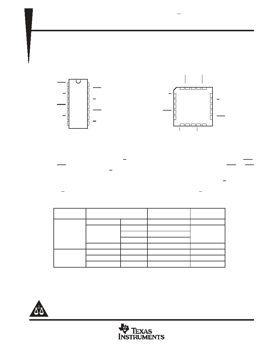
SN54HC109 . . . J OR W PACKAGE
SN74HC109 . . . D, N, OR NS PACKAGE
(TOP VIEW)
1
2
3
4
5
6
7
8
16
15
14
13
12
11
10
9
1CLR
1J
1K
1CLK
1PRE
1Q
1Q
GND
V
CC
2CLR
2J
2K
2CLK
2PRE
2Q
2Q
SN54HC109 . . . FK PACKAGE
(TOP VIEW)
NC - No internal connection
3
2 1 20 19
9 10 11 12 13
4
5
6
7
8
18
17
16
15
14
2J
2K
NC
2CLK
2PRE
1K
1CLK
NC
1PRE
1Q
1J
1CLR
NC
2Q
2Q
V
2CLR
1Q
GND
NC
CC
description/ordering information
These devices contain two independent J-K positive-edge-triggered flip-flops. A low level at the preset (PRE)
or clear (CLR) inputs sets or resets the outputs, regardless of the levels of the other inputs. When PRE and CLR
are inactive (high), data at the J and K inputs meeting the setup-time requirements are transferred to the outputs
on the positive-going edge of the clock (CLK) pulse. Clock triggering occurs at a voltage level and is not related
directly to the rise time of the clock pulse. Following the hold-time interval, data at the J and K inputs can be
changed without affecting the levels at the outputs. These versatile flip-flops can perform as toggle flip-flops by
grounding K and tying J high. They also can perform as D-type flip-flops if J and K are tied together.
ORDERING INFORMATION
TA
PACKAGE
ORDERABLE
PART NUMBER
TOP-SIDE
MARKING
PDIP - N
Tube of 25
SN74HC109N
SN74HC109N
Tube of 40
SN74HC109D
-40
∞
C to 85
∞
C
SOIC - D
Reel of 2500
SN74HC109DR
HC109
-40 C to 85 C
SOIC - D
Reel of 250
SN74HC109DT
HC109
SOP - NS
Reel of 2000
SN74HC109NSR
HC109
CDIP - J
Tube of 25
SNJ54HC109J
SNJ54HC109J
-55
∞
C to 125
∞
C
CFP - W
Tube of 150
SNJ54HC109W
SNJ54HC109W
-55 C to 125 C
LCCC - FK
Tube of 55
SNJ54HC109FK
SNJ54HC109FK
Package drawings, standard packing quantities, thermal data, symbolization, and PCB design guidelines are
available at www.ti.com/sc/package.
Copyright
2003, Texas Instruments Incorporated
Please be aware that an important notice concerning availability, standard warranty, and use in critical applications of
Texas Instruments semiconductor products and disclaimers thereto appears at the end of this data sheet.
PRODUCTION DATA information is current as of publication date.
Products conform to specifications per the terms of Texas Instruments
standard warranty. Production processing does not necessarily include
testing of all parameters.
On products compliant to MIL PRF 38535, all parameters are tested
unless otherwise noted. On all other products, production
processing does not necessarily include testing of all parameters.
SN54HC109, SN74HC109
DUAL J K POSITIVE EDGE TRIGGERED
FLIP FLOPS WITH CLEAR AND PRESET
SCLS470A - MARCH 2003 - REVISED OCTOBER 2003
2
POST OFFICE BOX 655303
∑
DALLAS, TEXAS 75265
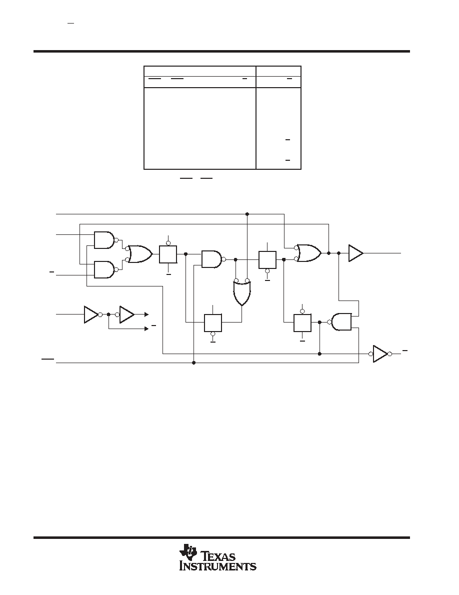
FUNCTION TABLE
INPUTS
OUTPUTS
PRE
CLR
CLK
J
K
Q
Q
L
H
X
X
X
H
L
H
L
X
X
X
L
H
L
L
X
X
X
H
H
H
H
L
L
L
H
H
H
H
L
Toggle
H
H
L
H
Q0
Q0
H
H
H
H
H
L
H
H
L
X
X
Q0
Q0
This configuration is nonstable; that is, it does not persist
when either PRE or CLR returns to its inactive (high) level.
logic diagram, each flip-flop (positive logic)
PRE
CLK
J
CLR
Q
Q
C
C
C
C
K
TG
TG
TG
TG
C
C
C
C
C
C
SN54HC109, SN74HC109
DUAL J K POSITIVE EDGE TRIGGERED
FLIP FLOPS WITH CLEAR AND PRESET
SCLS470A - MARCH 2003 - REVISED OCTOBER 2003
3
POST OFFICE BOX 655303
∑
DALLAS, TEXAS 75265
absolute maximum ratings over operating free-air temperature range (unless otherwise noted)
Supply voltage range, V
CC
-0.5 V to 7 V
. . . . . . . . . . . . . . . . . . . . . . . . . . . . . . . . . . . . . . . . . . . . . . . . . . . . . . . . . .
Input clamp current, I
IK
(V
I
< 0 or V
I
> V
CC
)
±
20 mA
. . . . . . . . . . . . . . . . . . . . . . . . . . . . . . . . . . . . . . . . . . . . . . . .
Output clamp current, I
OK
(V
O
< 0 or V
O
> V
CC
)
±
20 mA
. . . . . . . . . . . . . . . . . . . . . . . . . . . . . . . . . . . . . . . . . . . .
Continuous output current, I
O
(V
O
= 0 to V
CC
)
±
35 mA
. . . . . . . . . . . . . . . . . . . . . . . . . . . . . . . . . . . . . . . . . . . . . .
Continuous current through V
CC
or GND
±
70 mA
. . . . . . . . . . . . . . . . . . . . . . . . . . . . . . . . . . . . . . . . . . . . . . . . . . .
Package thermal impedance,
JA
(see Note 1): D package
73
∞
C/W
. . . . . . . . . . . . . . . . . . . . . . . . . . . . . . . . . . .
N package
67
∞
C/W
. . . . . . . . . . . . . . . . . . . . . . . . . . . . . . . . . . .
NS package
64
∞
C/W
. . . . . . . . . . . . . . . . . . . . . . . . . . . . . . . . .
Lead temperature 1,6 mm (1/16 inch) from case for 60 seconds: FK, J, or W packages
300
∞
C
. . . . . . . . . . .
Lead temperature 1,6 mm (1/16 inch) from case for 10 seconds: D, N, or NS packages
260
∞
C
. . . . . . . . . . .
Storage temperature range, T
stg
-65
∞
C to 150
∞
C
. . . . . . . . . . . . . . . . . . . . . . . . . . . . . . . . . . . . . . . . . . . . . . . . . . .
Stresses beyond those listed under "absolute maximum ratings" may cause permanent damage to the device. These are stress ratings only, and
functional operation of the device at these or any other conditions beyond those indicated under "recommended operating conditions" is not
implied. Exposure to absolute-maximum-rated conditions for extended periods may affect device reliability.
NOTE 1: The package thermal impedance is calculated in accordance with JESD 51-7.
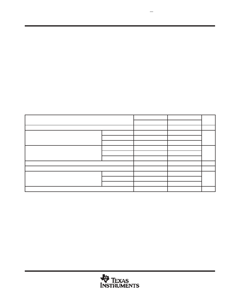
recommended operating conditions (see Note 2)
SN54HC109
SN74HC109
UNIT
MIN
NOM
MAX
MIN
NOM
MAX
UNIT
VCC
Supply voltage
2
5
6
2
5
6
V
VCC = 2 V
1.5
1.5
VIH
High-level input voltage
VCC = 4.5 V
3.15
3.15
V
VIH
High-level input voltage
VCC = 6 V
4.2
4.2
V
VCC = 2 V
0.3
0.5
VIL
Low-level input voltage
VCC = 4.5 V
0.9
1.35
V
VIL
Low-level input voltage
VCC = 6 V
1.2
1.8
V
VI
Input voltage
0
VCC
0
VCC
V
VO
Output voltage
0
VCC
0
VCC
V
VCC = 2 V
1000
1000
t/
v
Input transition rise/fall time
VCC = 4.5 V
500
500
ns
t/
v
Input transition rise/fall time
VCC = 6 V
400
400
ns
TA
Operating free-air temperature
-55
125
-40
85
∞
C
NOTE 2: All unused inputs of the device must be held at VCC or GND to ensure proper device operation. Refer to the TI application report,
Implications of Slow or Floating CMOS Inputs, literature number SCBA004.
SN54HC109, SN74HC109
DUAL J K POSITIVE EDGE TRIGGERED
FLIP FLOPS WITH CLEAR AND PRESET
SCLS470A - MARCH 2003 - REVISED OCTOBER 2003
4
POST OFFICE BOX 655303
∑
DALLAS, TEXAS 75265
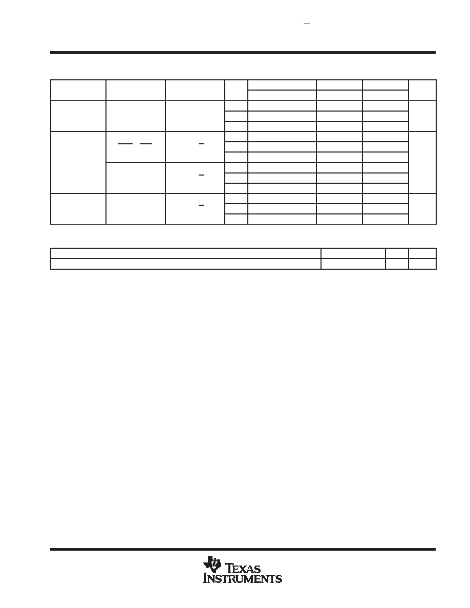
electrical characteristics over recommended operating free-air temperature range (unless
otherwise noted)
PARAMETER
TEST CONDITIONS
VCC
TA = 25
∞
C
SN54HC109
SN74HC109
UNIT
PARAMETER
TEST CONDITIONS
VCC
MIN
TYP
MAX
MIN
MAX
MIN
MAX
UNIT
2 V
1.9
1.998
1.9
1.9
IOH = -20
µ
A
4.5 V
4.4
4.499
4.4
4.4
VOH
VI = VIH or VIL
IOH = -20
µ
A
6 V
5.9
5.999
5.9
5.9
V
VOH
VI = VIH or VIL
IOH = -4 mA
4.5 V
3.98
4.3
3.7
3.84
V
IOH = -5.2 mA
6 V
5.48
5.8
5.2
5.34
2 V
0.002
0.1
0.1
0.1
IOL = 20
µ
A
4.5 V
0.001
0.1
0.1
0.1
VOL
VI = VIH or VIL
IOL = 20
µ
A
6 V
0.001
0.1
0.1
0.1
V
VOL
VI = VIH or VIL
IOL = 4 mA
4.5 V
0.17
0.26
0.4
0.33
V
IOL = 5.2 mA
6 V
0.15
0.26
0.4
0.33
II
VI = VCC or 0
6 V
±
0.1
±
100
±
1000
±
1000
nA
ICC
VI = VCC or 0,
IO = 0
6 V
4
80
40
µ
A
Ci
2 V to 6 V
3
10
10
10
pF
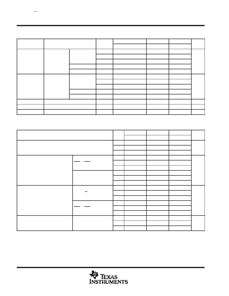
timing requirements over recommended operating free-air temperature range (unless otherwise
noted)
VCC
TA = 25
∞
C
SN54HC109
SN74HC109
UNIT
VCC
MIN
MAX
MIN
MAX
MIN
MAX
UNIT
2 V
6
4.2
5
fclock
Clock frequency
4.5 V
31
21
25
MHz
fclock
Clock frequency
6 V
36
25
29
MHz
2 V
100
150
125
PRE or CLR low
4.5 V
20
30
25
tw
Pulse duration
PRE or CLR low
6 V
17
25
21
ns
tw
Pulse duration
2 V
80
120
100
ns
CLK high or low
4.5 V
16
24
20
CLK high or low
6 V
14
20
17
2 V
100
150
125
Data (J, K)
4.5 V
20
30
25
tsu
Setup time before CLK
Data (J, K)
6 V
17
25
21
ns
tsu
Setup time before CLK
2 V
25
40
30
ns
PRE or CLR inactive
4.5 V
5
8
6
PRE or CLR inactive
6 V
4
7
5
2 V
0
0
0
th
Hold time
Data after CLK
4.5 V
0
0
0
ns
th
Hold time
Data after CLK
6 V
0
0
0
ns
SN54HC109, SN74HC109
DUAL J K POSITIVE EDGE TRIGGERED
FLIP FLOPS WITH CLEAR AND PRESET
SCLS470A - MARCH 2003 - REVISED OCTOBER 2003
5
POST OFFICE BOX 655303
∑
DALLAS, TEXAS 75265
switching characteristics over recommended operating free-air temperature range, C
L
= 50 pF
(unless otherwise noted) (see Figure 1)
PARAMETER
FROM
TO
VCC
TA = 25
∞
C
SN54HC109
SN74HC109
UNIT
PARAMETER
FROM
(INPUT)
TO
(OUTPUT)
VCC
MIN
TYP
MAX
MIN
MAX
MIN
MAX
UNIT
2 V
6
10
4.2
5
fmax
4.5 V
31
50
21
25
ns
fmax
6 V
36
60
25
29
ns
2 V
60
230
345
290
PRE or CLR
Q or Q
4.5 V
15
46
69
58
tpd
PRE or CLR
Q or Q
6 V
12
39
59
49
ns
tpd
2 V
50
175
250
220
ns
CLK
Q or Q
4.5 V
15
35
50
44
CLK
Q or Q
6 V
12
30
42
37
2 V
28
75
110
95
tt
Q or Q
4.5 V
8
15
22
19
ns
tt
Q or Q
6 V
6
13
19
16
ns
operating characteristics, T
A
= 25
∞
C
PARAMETER
TEST CONDITIONS
TYP
UNIT
Cpd
Power dissipation capacitance per buffer/driver
No load
35
pF
SN54HC109, SN74HC109
DUAL J K POSITIVE EDGE TRIGGERED
FLIP FLOPS WITH CLEAR AND PRESET
SCLS470A - MARCH 2003 - REVISED OCTOBER 2003
6
POST OFFICE BOX 655303
∑
DALLAS, TEXAS 75265
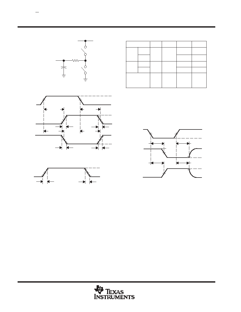
PARAMETER MEASUREMENT INFORMATION
VOLTAGE WAVEFORM
INPUT RISE AND FALL TIMES
50%
50%
10%
10%
90%
90%
VCC
0 V
tr
tf
Input
VOLTAGE WAVEFORMS
PROPAGATION DELAY AND OUTPUT TRANSITION TIMES
50%
50%
50%
10%
10%
90%
90%
VCC
VOH
VOL
0 V
tr
tf
Input
In-Phase
Output
50%
tPLH
tPHL
50%
50%
10%
10%
90%
90%
VOH
VOL
tr
tf
tPHL
tPLH
Out-of-Phase
Output
50%
10%
90%
VCC
VCC
VOL
0 V
Output
Control
(Low-Level
Enabling)
Output
Waveform 1
(See Note B)
50%
tPZL
tPLZ
VOLTAGE WAVEFORMS
ENABLE AND DISABLE TIMES FOR 3-STATE OUTPUTS
VOH
0 V
50%
50%
tPZH
tPHZ
Output
Waveform 2
(See Note B)
VCC
Test
Point
From Output
Under Test
CL
(see Note A)
RL
VCC
S1
S2
LOAD CIRCUIT
PARAMETER
CL
tPZH
tpd or tt
tdis
ten
tPZL
tPHZ
tPLZ
1 k
1 k
50 pF
or
150 pF
50 pF
Open
Closed
RL
S1
Closed
Open
S2
Open
Closed
Closed
Open
50 pF
or
150 pF
Open
Open
--
NOTES: A. CL includes probe and test-fixture capacitance.
B. Waveform 1 is for an output with internal conditions such that the output is low except when disabled by the output control.
Waveform 2 is for an output with internal conditions such that the output is high except when disabled by the output control.
C. Phase relationships between waveforms were chosen arbitrarily. All input pulses are supplied by generators having the following
characteristics: PRR
1 MHz, ZO = 50
, tr = 6 ns, tf = 6 ns.
D. The outputs are measured one at a time with one input transition per measurement.
E. tPLZ and tPHZ are the same as tdis.
F. tPZL and tPZH are the same as ten.
G. tPLH and tPHL are the same as tpd.
Figure 1. Load Circuit and Voltage Waveforms
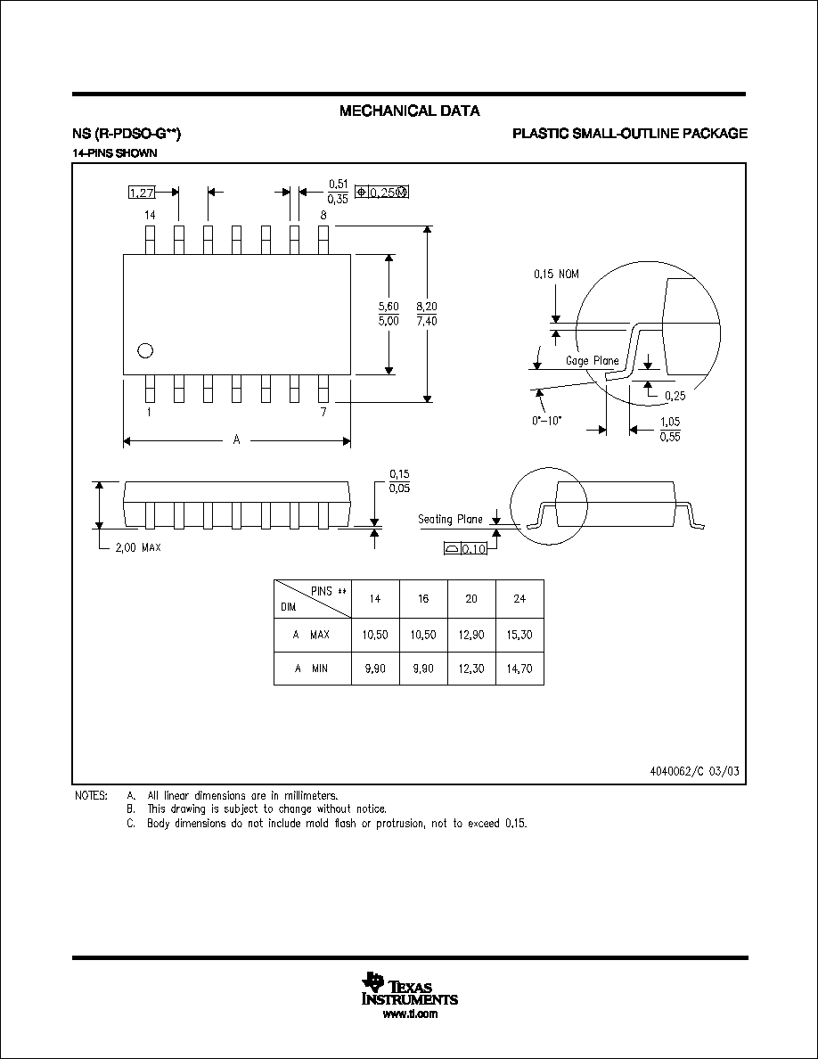
MECHANICAL DATA
MCFP004A≠ JANUARY 1995 ≠ REVISED FEBRUARY 2002
1
POST OFFICE BOX 655303
∑
DALLAS, TEXAS 75265
W (R-GDFP-F16)
CERAMIC DUAL FLATPACK
0.360 (9,14)
0.250 (6,35)
9
8
16
1
0.245 (6,22)
0.004 (0,10)
0.026 (0,66)
4 Places
0.015 (0,38)
0.055 (1,40)
0.370 (9,40)
0.006 (0,15)
0.045 (1,14)
Base and Seating Plane
0.005 (0,13) MIN
0.019 (0,48)
0.430 (10,92)
0.285 (7,24)
0.080 (2,03)
4040180-3 / C 02/02
0.305 (7,75) MAX
0.050 (1,27)
0.360 (9,14)
0.250 (6,35)
NOTES: A. All linear dimensions are in inches (millimeters).
B. This drawing is subject to change without notice.
C. This package can be hermetically sealed with a ceramic lid using glass frit.
D. Index point is provided on cap for terminal identification only.
E. Falls within MIL STD 1835 GDFP-1F16 and JEDEC MO-092AC
MECHANICAL DATA
MLCC006B ≠ OCTOBER 1996
1
POST OFFICE BOX 655303
∑
DALLAS, TEXAS 75265
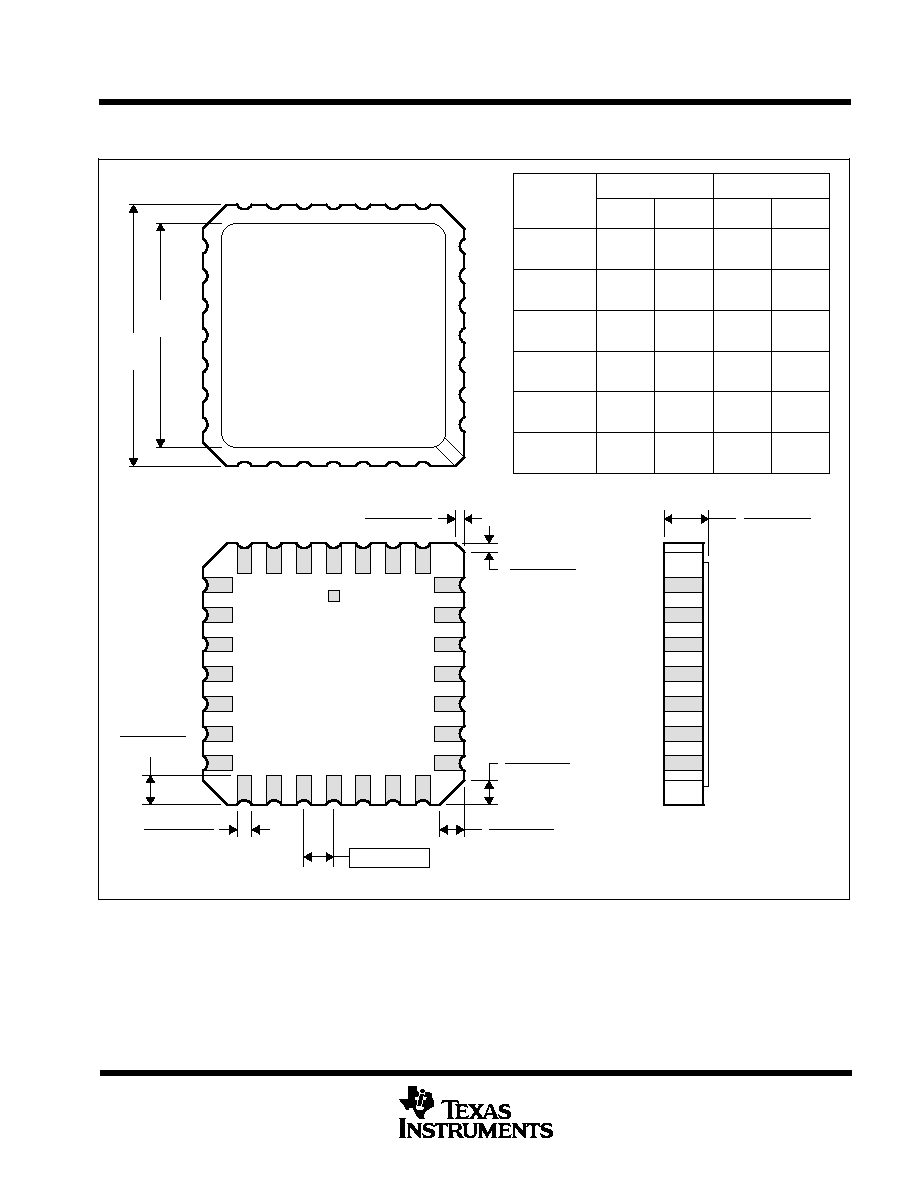
FK (S-CQCC-N**)
LEADLESS CERAMIC CHIP CARRIER
4040140 / D 10/96
28 TERMINAL SHOWN
B
0.358
(9,09)
MAX
(11,63)
0.560
(14,22)
0.560
0.458
0.858
(21,8)
1.063
(27,0)
(14,22)
A
NO. OF
MIN
MAX
0.358
0.660
0.761
0.458
0.342
(8,69)
MIN
(11,23)
(16,26)
0.640
0.739
0.442
(9,09)
(11,63)
(16,76)
0.962
1.165
(23,83)
0.938
(28,99)
1.141
(24,43)
(29,59)
(19,32)
(18,78)
**
20
28
52
44
68
84
0.020 (0,51)
TERMINALS
0.080 (2,03)
0.064 (1,63)
(7,80)
0.307
(10,31)
0.406
(12,58)
0.495
(12,58)
0.495
(21,6)
0.850
(26,6)
1.047
0.045 (1,14)
0.045 (1,14)
0.035 (0,89)
0.035 (0,89)
0.010 (0,25)
12
13
14
15
16
18
17
11
10
8
9
7
5
4
3
2
0.020 (0,51)
0.010 (0,25)
6
1
28
26
27
19
21
B SQ
A SQ
22
23
24
25
20
0.055 (1,40)
0.045 (1,14)
0.028 (0,71)
0.022 (0,54)
0.050 (1,27)
NOTES: A. All linear dimensions are in inches (millimeters).
B. This drawing is subject to change without notice.
C. This package can be hermetically sealed with a metal lid.
D. The terminals are gold plated.
E. Falls within JEDEC MS-004
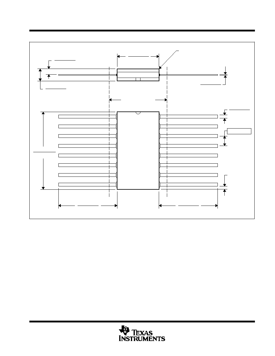
MECHANICAL
MPDI002C ≠ JANUARY 1995 ≠ REVISED DECEMBER 20002
1
POST OFFICE BOX 655303
∑
DALLAS, TEXAS 75265
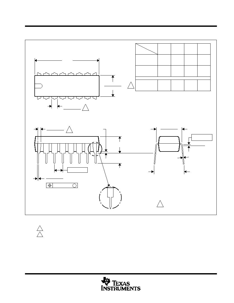
N (R-PDIP-T**)
PLASTIC DUAL-IN-LINE PACKAGE
BB
AC
AD
0.325 (8,26)
0.300 (7,62)
0.010 (0,25) NOM
Gauge Plane
0.015 (0,38)
0.430 (10,92) MAX
20
1.060
(26,92)
0.940
(23,88)
18
0.920
0.850
14
0.775
0.745
(19,69)
(18,92)
16
0.775
(19,69)
(18,92)
0.745
A MIN
DIM
A MAX
PINS **
(23,37)
(21,59)
Seating Plane
14/18 PIN ONLY
20 pin vendor option
4040049/E 12/2002
9
8
0.070 (1,78)
A
0.045 (1,14)
0.020 (0,51) MIN
16
1
0.015 (0,38)
0.021 (0,53)
0.200 (5,08) MAX
0.125 (3,18) MIN
0.240 (6,10)
0.260 (6,60)
M
0.010 (0,25)
0.100 (2,54)
16 PINS SHOWN
MS-100
VARIATION
AA
C
D
D
D
0.030 (0,76)
0.045 (1,14)
NOTES: A. All linear dimensions are in inches (millimeters).
B. This drawing is subject to change without notice.
C. Falls within JEDEC MS-001, except 18 and 20 pin minimum body lrngth (Dim A).
D. The 20 pin end lead shoulder width is a vendor option, either half or full width.
MECHANICAL DATA
MSOI002B ≠ JANUARY 1995 ≠ REVISED SEPTEMBER 2001
1
POST OFFICE BOX 655303
∑
DALLAS, TEXAS 75265
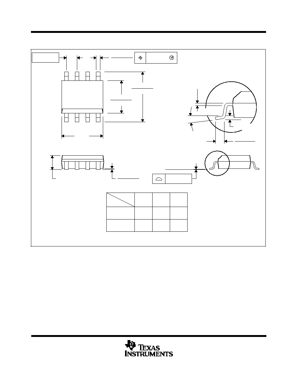
D (R-PDSO-G**)
PLASTIC SMALL-OUTLINE PACKAGE
8 PINS SHOWN
8
0.197
(5,00)
A MAX
A MIN
(4,80)
0.189
0.337
(8,55)
(8,75)
0.344
14
0.386
(9,80)
(10,00)
0.394
16
DIM
PINS **
4040047/E 09/01
0.069 (1,75) MAX
Seating Plane
0.004 (0,10)
0.010 (0,25)
0.010 (0,25)
0.016 (0,40)
0.044 (1,12)
0.244 (6,20)
0.228 (5,80)
0.020 (0,51)
0.014 (0,35)
1
4
8
5
0.150 (3,81)
0.157 (4,00)
0.008 (0,20) NOM
0
∞
≠ 8
∞
Gage Plane
A
0.004 (0,10)
0.010 (0,25)
0.050 (1,27)
NOTES: A. All linear dimensions are in inches (millimeters).
B. This drawing is subject to change without notice.
C. Body dimensions do not include mold flash or protrusion, not to exceed 0.006 (0,15).
D. Falls within JEDEC MS-012

IMPORTANT NOTICE
Texas Instruments Incorporated and its subsidiaries (TI) reserve the right to make corrections, modifications,
enhancements, improvements, and other changes to its products and services at any time and to discontinue
any product or service without notice. Customers should obtain the latest relevant information before placing
orders and should verify that such information is current and complete. All products are sold subject to TI's terms
and conditions of sale supplied at the time of order acknowledgment.
TI warrants performance of its hardware products to the specifications applicable at the time of sale in
accordance with TI's standard warranty. Testing and other quality control techniques are used to the extent TI
deems necessary to support this warranty. Except where mandated by government requirements, testing of all
parameters of each product is not necessarily performed.
TI assumes no liability for applications assistance or customer product design. Customers are responsible for
their products and applications using TI components. To minimize the risks associated with customer products
and applications, customers should provide adequate design and operating safeguards.
TI does not warrant or represent that any license, either express or implied, is granted under any TI patent right,
copyright, mask work right, or other TI intellectual property right relating to any combination, machine, or process
in which TI products or services are used. Information published by TI regarding third-party products or services
does not constitute a license from TI to use such products or services or a warranty or endorsement thereof.
Use of such information may require a license from a third party under the patents or other intellectual property
of the third party, or a license from TI under the patents or other intellectual property of TI.
Reproduction of information in TI data books or data sheets is permissible only if reproduction is without
alteration and is accompanied by all associated warranties, conditions, limitations, and notices. Reproduction
of this information with alteration is an unfair and deceptive business practice. TI is not responsible or liable for
such altered documentation.
Resale of TI products or services with statements different from or beyond the parameters stated by TI for that
product or service voids all express and any implied warranties for the associated TI product or service and
is an unfair and deceptive business practice. TI is not responsible or liable for any such statements.
Following are URLs where you can obtain information on other Texas Instruments products and application
solutions:
Products
Applications
Amplifiers
amplifier.ti.com
Audio
www.ti.com/audio
Data Converters
dataconverter.ti.com
Automotive
www.ti.com/automotive
DSP
dsp.ti.com
Broadband
www.ti.com/broadband
Interface
interface.ti.com
Digital Control
www.ti.com/digitalcontrol
Logic
logic.ti.com
Military
www.ti.com/military
Power Mgmt
power.ti.com
Optical Networking
www.ti.com/opticalnetwork
Microcontrollers
microcontroller.ti.com
Security
www.ti.com/security
Telephony
www.ti.com/telephony
Video & Imaging
www.ti.com/video
Wireless
www.ti.com/wireless
Mailing Address:
Texas Instruments
Post Office Box 655303 Dallas, Texas 75265
Copyright
2003, Texas Instruments Incorporated