 | –≠–ª–µ–∫—Ç—Ä–æ–Ω–Ω—ã–π –∫–æ–º–ø–æ–Ω–µ–Ω—Ç: 85124012A | –°–∫–∞—á–∞—Ç—å:  PDF PDF  ZIP ZIP |
SN54HC257, SN54HC258, SN74HC257, SN74HC258
QUADRUPLE 2 LINE TO 1 LINE DATA SELECTORS/MULTIPLEXERS
WITH 3 STATE OUTPUTS
SCLS224B - DECEMBER 1982 - REVISED SEPTEMBER 2003
1
POST OFFICE BOX 655303
∑
DALLAS, TEXAS 75265
D
Wide Operating Voltage Range of 2 V to 6 V
D
High-Current Inverting Outputs Drive Up To
15 LSTTL Loads
D
Low Power Consumption, 80-
µ
A Max I
CC
D
'HC257 . . . Typical t
pd
= 9 ns
D
'HC258 . . . Typical t
pd
= 12 ns
D
±
6-mA Output Drive at 5 V
D
Low Input Current of 1
µ
A Max
D
Provides Bus Interface from Multiple
Sources in High-Performance Systems
1
2
3
4
5
6
7
8
16
15
14
13
12
11
10
9
A/B
1A
1B
1Y
2A
2B
2Y
GND
V
CC
G
4A
4B
4Y
3A
3B
3Y
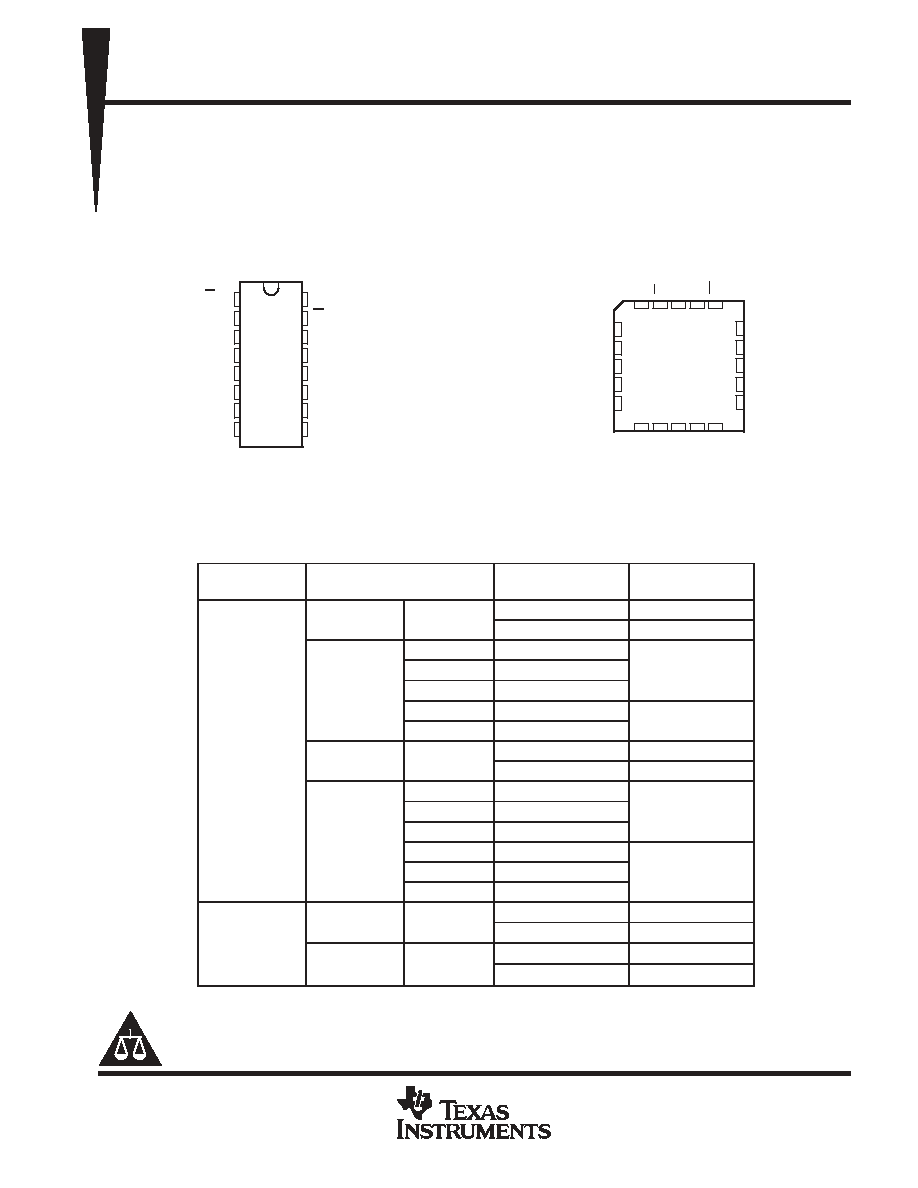
SN54HC257, SN54HC258 . . . J PACKAGE
SN74HC257, SN74HC258 . . . D, N, NS, OR PW PACKAGE
(TOP VIEW)
3
2 1 20 19
9 10 11 12 13
4
5
6
7
8
18
17
16
15
14
4A
4B
NC
4Y
3A
SN54HC257, SN54HC258 . . . FK PACKAGE
(TOP VIEW)
1A
A/B
NC
3Y
3B
V
G
2Y
GND
NC
CC
NC - No internal connection
1B
1Y
NC
2A
2B
description/ordering information
ORDERING INFORMATION
TA
PACKAGE
ORDERABLE
PART NUMBER
TOP-SIDE
MARKING
PDIP - N
Tube of 25
SN74HC257N
SN74HC257N
PDIP - N
Tube of 25
SN74HC258N
SN74HC258N
Tube of 40
SN74HC257D
Reel of 2500
SN74HC257DR
HC257
SOIC - D
Reel of 250
SN74HC257DT
HC257
SOIC - D
Tube of 40
SN74HC258D
HC258
Reel of 2500
SN74HC258DR
HC258
-40
∞
C to 85
∞
C
SOP - NS
Reel of 2000
SN74HC257NSR
HC257
-40 C to 85 C
SOP - NS
Reel of 2000
SN74HC258NSR
HC258
Tube of 90
SN74HC257PW
Reel of 2000
SN74HC257PWR
HC257
TSSOP - PW
Reel of 250
SN74HC257PWT
HC257
TSSOP - PW
Tube of 90
SN74HC258PW
Reel of 2000
SN74HC258PWR
HC258
Reel of 250
SN74HC258PWT
HC258
CDIP - J
Tube of 25
SNJ54HC257J
SNJ54HC257J
-55
∞
C to 125
∞
C
CDIP - J
Tube of 25
SNJ54HC258J
SNJ54HC258J
-55
∞
C to 125
∞
C
LCCC - FK
Tube of 55
SNJ54HC257FK
SNJ54HC257FK
LCCC - FK
Tube of 55
SNJ54HC258FK
SNJ54HC258FK
Package drawings, standard packing quantities, thermal data, symbolization, and PCB design guidelines
are available at www.ti.com/sc/package.
Copyright
2003, Texas Instruments Incorporated
PRODUCTION DATA information is current as of publication date.
Products conform to specifications per the terms of Texas Instruments
standard warranty. Production processing does not necessarily include
testing of all parameters.
Please be aware that an important notice concerning availability, standard warranty, and use in critical applications of
Texas Instruments semiconductor products and disclaimers thereto appears at the end of this data sheet.
On products compliant to MIL PRF 38535, all parameters are tested
unless otherwise noted. On all other products, production
processing does not necessarily include testing of all parameters.

SN54HC257, SN54HC258, SN74HC257, SN74HC258
QUADRUPLE 2 LINE TO 1 LINE DATA SELECTORS/MULTIPLEXERS
WITH 3 STATE OUTPUTS
SCLS224B - DECEMBER 1982 - REVISED SEPTEMBER 2003
2
POST OFFICE BOX 655303
∑
DALLAS, TEXAS 75265
description/ordering information (continued)
These devices are designed to multiplex signals from 4-bit data sources to 4-output data lines in bus-organized
systems. The 3-state outputs do not load the data lines when the output-enable (G) input is at a high logic level.
To ensure the high-impedance state during power up or power down, G should be tied to V
CC
through a pullup
resistor; the minimum value of the resistor is determined by the current-sinking capability of the driver.
FUNCTION TABLE
INPUTS
OUTPUT Y
G
A/B
A
B
'HC257
'HC258
H
X
X
X
Z
Z
L
L
L
X
L
H
L
L
H
X
H
L
L
H
X
L
L
H
L
H
X
H
H
L
'HC257 logic diagram (positive logic)
4Y
3Y
2Y
1Y
A/B
G
4B
4A
3B
3A
2B
2A
1B
1A
4
2
3
7
5
6
9
11
10
12
14
13
1
15
Pin numbers shown are for the D, J, N, NS, and PW packages.

SN54HC257, SN54HC258, SN74HC257, SN74HC258
QUADRUPLE 2 LINE TO 1 LINE DATA SELECTORS/MULTIPLEXERS
WITH 3 STATE OUTPUTS
SCLS224B - DECEMBER 1982 - REVISED SEPTEMBER 2003
3
POST OFFICE BOX 655303
∑
DALLAS, TEXAS 75265
'HC258 logic diagram (positive logic)
4Y
3Y
2Y
1Y
A/B
G
4B
4A
3B
3A
2B
2A
1B
1A
4
2
3
7
5
6
9
11
10
12
14
13
1
15
Pin numbers shown are for the D, J, N, NS, and PW packages.
absolute maximum ratings over operating free-air temperature range (unless otherwise noted)
Supply voltage range, V
CC
-0.5 V to 7 V
. . . . . . . . . . . . . . . . . . . . . . . . . . . . . . . . . . . . . . . . . . . . . . . . . . . . . . . . . .
Input clamp current, I
IK
(V
I
< 0 or V
I
> V
CC
)
±
20 mA
. . . . . . . . . . . . . . . . . . . . . . . . . . . . . . . . . . . . . . . . . . . . . . . .
Output clamp current, I
OK
(V
O
< 0 or V
O
> V
CC
)
±
20 mA
. . . . . . . . . . . . . . . . . . . . . . . . . . . . . . . . . . . . . . . . . . . .
Continuous output current, I
O
(V
O
= 0 to V
CC
)
±
35 mA
. . . . . . . . . . . . . . . . . . . . . . . . . . . . . . . . . . . . . . . . . . . . . .
Continuous current through V
CC
or GND
±
70 mA
. . . . . . . . . . . . . . . . . . . . . . . . . . . . . . . . . . . . . . . . . . . . . . . . . . .
Package thermal impedance,
JA
(see Note 1): D package
73
∞
C/W
. . . . . . . . . . . . . . . . . . . . . . . . . . . . . . . . . . .
N package
67
∞
C/W
. . . . . . . . . . . . . . . . . . . . . . . . . . . . . . . . . . .
NS package
64
∞
C/W
. . . . . . . . . . . . . . . . . . . . . . . . . . . . . . . . .
PW package
108
∞
C/W
. . . . . . . . . . . . . . . . . . . . . . . . . . . . . . . .
Storage temperature range, T
stg
-65
∞
C to 150
∞
C
. . . . . . . . . . . . . . . . . . . . . . . . . . . . . . . . . . . . . . . . . . . . . . . . . . .
Stresses beyond those listed under "absolute maximum ratings" may cause permanent damage to the device. These are stress ratings only, and
functional operation of the device at these or any other conditions beyond those indicated under "recommended operating conditions" is not
implied. Exposure to absolute-maximum-rated conditions for extended periods may affect device reliability.
NOTE 1: The package thermal impedance is calculated in accordance with JESD 51-7.

SN54HC257, SN54HC258, SN74HC257, SN74HC258
QUADRUPLE 2 LINE TO 1 LINE DATA SELECTORS/MULTIPLEXERS
WITH 3 STATE OUTPUTS
SCLS224B - DECEMBER 1982 - REVISED SEPTEMBER 2003
4
POST OFFICE BOX 655303
∑
DALLAS, TEXAS 75265
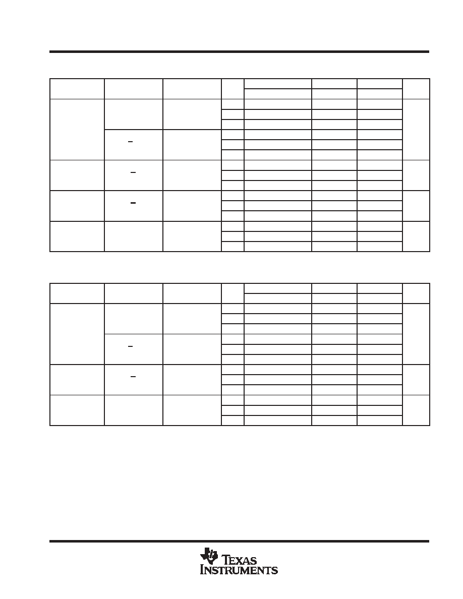
recommended operating conditions (see Note 2)
SN54HC257,
SN54HC258
SN74HC257,
SN74HC258
UNIT
MIN
NOM
MAX
MIN
NOM
MAX
UNIT
VCC
Supply voltage
2
5
6
2
5
6
V
VCC = 2 V
1.5
1.5
VIH
High-level input voltage
VCC = 4.5 V
3.15
3.15
V
VIH
High-level input voltage
VCC = 6 V
4.2
4.2
V
VCC = 2 V
0.3
0.5
VIL
Low-level input voltage
VCC = 4.5 V
0.9
1.35
V
VIL
Low-level input voltage
VCC = 6 V
1.2
1.8
V
VI
Input voltage
0
VCC
0
VCC
V
VO
Output voltage
0
VCC
0
VCC
V
VCC = 2 V
1000
1000
t/
v
Input transition rise/fall time
VCC = 4.5 V
500
500
ns
t/
v
Input transition rise/fall time
VCC = 6 V
400
400
ns
TA
Operating free-air temperature
-55
125
-40
85
∞
C
NOTE 2: All unused inputs of the device must be held at VCC or GND to ensure proper device operation. Refer to the TI application report,
Implications of Slow or Floating CMOS Inputs, literature number SCBA004.
electrical characteristics over recommended operating free-air temperature range (unless
otherwise noted)
PARAMETER
TEST CONDITIONS
VCC
TA = 25
∞
C
SN54HC257,
SN54HC258
SN74HC257,
SN74HC258
UNIT
PARAMETER
TEST CONDITIONS
VCC
MIN
TYP
MAX
MIN
MAX
MIN
MAX
UNIT
2 V
1.9
1.998
1.9
1.9
IOH = -20
µ
A
4.5 V
4.4
4.499
4.4
4.4
VOH
VI = VIH or VIL
IOH = -20
µ
A
6 V
5.9
5.999
5.9
5.9
V
VOH
VI = VIH or VIL
IOH = -6 mA
4.5 V
3.98
4.3
3.7
3.84
V
IOH = -7.8 mA
6 V
5.48
5.8
5.2
5.34
2 V
0.002
0.1
0.1
0.1
IOL = 20
µ
A
4.5 V
0.001
0.1
0.1
0.1
VOL
VI = VIH or VIL
IOL = 20
µ
A
6 V
0.001
0.1
0.1
0.1
V
VOL
VI = VIH or VIL
IOL = 6 mA
4.5 V
0.17
0.26
0.4
0.33
V
IOL = 7.8 mA
6 V
0.15
0.26
0.4
0.33
II
VI = VCC or 0
6 V
±
0.1
±
100
±
1000
±
1000
nA
IOZ
VO = VCC or 0
6 V
±
0.01
±
0.5
±
10
±
5
µ
A
ICC
VI = VCC or 0,
IO = 0
6 V
8
160
80
µ
A
Ci
2 V to 6 V
3
10
10
10
pF
SN54HC257, SN54HC258, SN74HC257, SN74HC258
QUADRUPLE 2 LINE TO 1 LINE DATA SELECTORS/MULTIPLEXERS
WITH 3 STATE OUTPUTS
SCLS224B - DECEMBER 1982 - REVISED SEPTEMBER 2003
5
POST OFFICE BOX 655303
∑
DALLAS, TEXAS 75265
switching characteristics over recommended operating free-air temperature range, C
L
= 50 pF
(unless otherwise noted) (see Figure 1)
PARAMETER
FROM
TO
VCC
TA = 25
∞
C
SN54HC257
SN74HC257
UNIT
PARAMETER
FROM
(INPUT)
TO
(OUTPUT)
VCC
MIN
TYP
MAX
MIN
MAX
MIN
MAX
UNIT
2 V
50
100
150
125
A or B
Any Y
4.5 V
10
20
30
25
tpd
A or B
Any Y
6 V
9
17
25
21
ns
tpd
2 V
50
100
150
125
ns
A/B
Any Y
4.5 V
10
20
30
25
A/B
Any Y
6 V
9
17
25
21
2 V
75
150
225
190
ten
G
Any Y
4.5 V
15
30
45
38
ns
ten
G
Any Y
6 V
13
26
38
32
ns
2 V
75
150
225
190
tdis
G
Any Y
4.5 V
15
30
45
38
ns
tdis
G
Any Y
6 V
13
26
38
32
ns
2 V
28
60
90
75
tt
Any Y
4.5 V
8
12
18
15
ns
tt
Any Y
6 V
6
10
15
13
ns
switching characteristics over recommended operating free-air temperature range, C
L
= 150 pF
(unless otherwise noted) (see Figure 1)
PARAMETER
FROM
TO
VCC
TA = 25
∞
C
SN54HC257
SN74HC257
UNIT
PARAMETER
FROM
(INPUT)
TO
(OUTPUT)
VCC
MIN
TYP
MAX
MIN
MAX
MIN
MAX
UNIT
2 V
75
150
245
190
A or B
Any Y
4.5 V
15
30
45
38
tpd
A or B
Any Y
6 V
13
26
38
32
ns
tpd
2 V
75
150
245
190
ns
A/B
Any Y
4.5 V
15
30
45
38
A/B
Any Y
6 V
13
26
38
32
2 V
100
200
300
250
ten
G
Any Y
4.5 V
24
40
60
50
ns
ten
G
Any Y
6 V
18
34
51
43
ns
2 V
45
210
315
265
tt
Any Y
4.5 V
17
42
63
53
ns
tt
Any Y
6 V
13
36
53
45
ns