 | –≠–ª–µ–∫—Ç—Ä–æ–Ω–Ω—ã–π –∫–æ–º–ø–æ–Ω–µ–Ω—Ç: 85506012A | –°–∫–∞—á–∞—Ç—å:  PDF PDF  ZIP ZIP |

SN54HCT245, SN74HCT245
OCTAL BUS TRANSCEIVERS
WITH 3-STATE OUTPUTS
SCLS020E ≠ MARCH 1984 ≠ REVISED AUGUST 2003
1
POST OFFICE BOX 655303
∑
DALLAS, TEXAS 75265
D
Operating Voltage Range of 4.5 V to 5.5 V
D
High-Current 3-State Outputs Drive Bus
Lines Directly or Up To 15 LSTTL Loads
D
Low Power Consumption, 80-
µ
A Max I
CC
D
Typical t
pd
= 14 ns
D
±
6-mA Output Drive at 5 V
D
Low Input Current of 1
µ
A Max
D
Inputs Are TTL-Voltage Compatible
description/ordering information
These octal bus transceivers are designed for
asynchronous two-way communication between
data buses. The control-function implementation
minimizes external timing requirements.
The 'HCT245 devices allow data transmission
from the A bus to the B bus or from the B bus to the
A bus, depending upon the logic level at the
direction-control (DIR) input. The output-enable
(OE) input can be used to disable the device so
that the buses are effectively isolated.
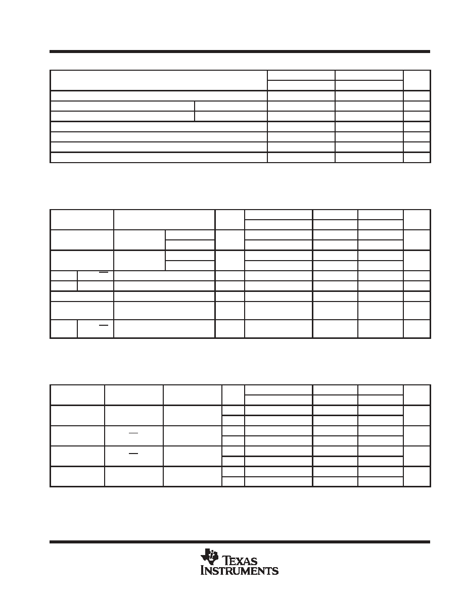
ORDERING INFORMATION
TA
PACKAGE
ORDERABLE
PART NUMBER
TOP-SIDE
MARKING
≠40 C to 85 C
PDIP ≠ N
Tube of 20
SN74HCT245N
SN74HCT245N
≠40 C to 85 C
SOIC ≠ DW
Tube of 25
SN74HCT245DW
HCT245
≠40 C to 85 C
SOIC ≠ DW
Reel of 2000
SN74HCT245DWR
HCT245
≠40
∞
C to 85
∞
C
SOP ≠ NS
Reel of 2000
SN74HCT245NSR
HCT245
≠40
∞
C to 85
∞
C
SSOP ≠ DB
Reel of 2000
SN74HCT245DBR
HT245
TSSOP ≠ PW
Tube of 70
SN74HCT245PW
HT245
TSSOP ≠ PW
Reel of 2000
SN74HCT245PWR
HT245
Reel of 250
SN74HCT245PWT
≠55 C to 125 C
CDIP ≠ J
Tube of 20
SNJ54HCT245J
SNJ54HCT245J
≠55
∞
C to 125
∞
C
CFP ≠ W
Tube of 85
SNJ54HCT245W
SNJ54HCT245W
LCCC ≠ FK
Tube of 55
SNJ54HCT245FK
SNJ54HCT245FK
Package drawings, standard packing quantities, thermal data, symbolization, and PCB design guidelines are
available at www.ti.com/sc/package.
Please be aware that an important notice concerning availability, standard warranty, and use in critical applications of
Texas Instruments semiconductor products and disclaimers thereto appears at the end of this data sheet.
3
2
1 20 19
9 10 11 12 13
4
5
6
7
8
18
17
16
15
14
B1
B2
B3
B4
B5
A3
A4
A5
A6
A7
A2
A1
DIR
B7
B6
OE
A8
GND
B8
V
CC
SN54HCT245 . . . FK PACKAGE
(TOP VIEW)
1
2
3
4
5
6
7
8
9
10
20
19
18
17
16
15
14
13
12
11
DIR
A1
A2
A3
A4
A5
A6
A7
A8
GND
V
CC
OE
B1
B2
B3
B4
B5
B6
B7
B8
SN54HCT245 . . . J OR W PACKAGE
SN74HCT245 . . . DB, DW, N, NS, OR PW PACKAGE
(TOP VIEW)
Copyright
2003, Texas Instruments Incorporated
PRODUCTION DATA information is current as of publication date.
Products conform to specifications per the terms of Texas Instruments
standard warranty. Production processing does not necessarily include
testing of all parameters.
On products compliant to MIL-PRF-38535, all parameters are tested
unless otherwise noted. On all other products, production
processing does not necessarily include testing of all parameters.

SN54HCT245, SN74HCT245
OCTAL BUS TRANSCEIVERS
WITH 3-STATE OUTPUTS
SCLS020E ≠ MARCH 1984 ≠ REVISED AUGUST 2003
2
POST OFFICE BOX 655303
∑
DALLAS, TEXAS 75265
FUNCTION TABLE
INPUTS
OPERATION
OE
DIR
OPERATION
L
L
B data to A bus
L
H
A data to B bus
H
X
Isolation
logic diagram (positive logic)
DIR
OE
A1
B1
1
2
18
19
To Seven Other Channels
absolute maximum ratings over operating free-air temperature range (unless otherwise noted)
Supply voltage range, V
CC
≠0.5 V to 7 V
. . . . . . . . . . . . . . . . . . . . . . . . . . . . . . . . . . . . . . . . . . . . . . . . . . . . . . . . . .
Input clamp current, I
IK
(V
I
< 0 or V
I
> V
CC
) (see Note 1)
±
20 mA
. . . . . . . . . . . . . . . . . . . . . . . . . . . . . . . . . . . .
Output clamp current, I
OK
(V
O
< 0 or V
O
> V
CC
) (see Note 1)
±
20 mA
. . . . . . . . . . . . . . . . . . . . . . . . . . . . . . . .
Continuous output current, I
O
(V
O
= 0 to V
CC
)
±
35 mA
. . . . . . . . . . . . . . . . . . . . . . . . . . . . . . . . . . . . . . . . . . . . . .
Continuous current through V
CC
or GND
±
70 mA
. . . . . . . . . . . . . . . . . . . . . . . . . . . . . . . . . . . . . . . . . . . . . . . . . . .
Package thermal impedance,
JA
(see Note 2): DB package
70
∞
C/W
. . . . . . . . . . . . . . . . . . . . . . . . . . . . . . . . .
DW package
58
∞
C/W
. . . . . . . . . . . . . . . . . . . . . . . . . . . . . . . . .
N package
69
∞
C/W
. . . . . . . . . . . . . . . . . . . . . . . . . . . . . . . . . . .
NS package
60
∞
C/W
. . . . . . . . . . . . . . . . . . . . . . . . . . . . . . . . .
PW package
83
∞
C/W
. . . . . . . . . . . . . . . . . . . . . . . . . . . . . . . . .
Storage temperature range, T
stg
≠65
∞
C to 150
∞
C
. . . . . . . . . . . . . . . . . . . . . . . . . . . . . . . . . . . . . . . . . . . . . . . . . . .
Stresses beyond those listed under "absolute maximum ratings" may cause permanent damage to the device. These are stress ratings only, and
functional operation of the device at these or any other conditions beyond those indicated under "recommended operating conditions" is not
implied. Exposure to absolute-maximum-rated conditions for extended periods may affect device reliability.
NOTES:
1. The input and output voltage ratings may be exceeded if the input and output current ratings are observed.
2. The package thermal impedance is calculated in accordance with JESD 51-7.
SN54HCT245, SN74HCT245
OCTAL BUS TRANSCEIVERS
WITH 3-STATE OUTPUTS
SCLS020E ≠ MARCH 1984 ≠ REVISED AUGUST 2003
3
POST OFFICE BOX 655303
∑
DALLAS, TEXAS 75265
recommended operating conditions (see Note 3)
SN54HCT245
SN74HCT245
UNIT
MIN
NOM
MAX
MIN
NOM
MAX
UNIT
VCC
Supply voltage
4.5
5
5.5
4.5
5
5.5
V
VIH
High-level input voltage
VCC = 4.5 V to 5.5 V
2
2
V
VIL
Low-level input voltage
VCC = 4.5 V to 5.5 V
0.8
0.8
V
VI
Input voltage
0
VCC
0
VCC
V
VO
Output voltage
0
VCC
0
VCC
V
t/
v
Input transition rise/fall time
500
500
ns
TA
Operating free-air temperature
≠55
125
≠40
85
∞
C
NOTE 3: All unused inputs of the device must be held at VCC or GND to ensure proper device operation. Refer to the TI application report,
Implications of Slow or Floating CMOS Inputs, literature number SCBA004.
electrical characteristics over recommended operating free-air temperature range (unless
otherwise noted)
PARAMETER
TEST CONDITIONS
VCC
TA = 25
∞
C
SN54HCT245
SN74HCT245
UNIT
PARAMETER
TEST CONDITIONS
VCC
MIN
TYP
MAX
MIN
MAX
MIN
MAX
UNIT
VOH
VI = VIH or VIL
IOH = ≠20
µ
A
4.5 V
4.4
4.499
4.4
4.4
V
VOH
VI = VIH or VIL
IOH = ≠6 mA
4.5 V
3.98
4.3
3.7
3.84
V
VOL
VI = VIH or VIL
IOL = 20
µ
A
4.5 V
0.001
0.1
0.1
0.1
V
VOL
VI = VIH or VIL
IOL = 6 mA
4.5 V
0.17
0.26
0.4
0.33
V
II
DIR or OE
VI = VCC or 0
5.5 V
±
0.1
±
100
±
1000
±
1000
nA
IOZ
A or B
VO = VCC or 0
5.5 V
±
0.01
±
0.5
±
10
±
5
µ
A
ICC
VI = VCC or 0,
IO = 0
5.5 V
8
160
80
µ
A
ICC
One input at 0.5 V or 2.4 V,
Other inputs at 0 or VCC
5.5 V
1.4
2.4
3
2.9
mA
Ci
DIR or OE
4.5 V
to 5.5 V
3
10
10
10
pF
This is the increase in supply current for each input that is at one of the specified TTL voltage levels, rather than 0 V or VCC.
Parameter Ci does not apply to transceiver I/O ports.
switching characteristics over recommended operating free-air temperature range, C
L
= 50 pF
(unless otherwise noted) (see Figure 1)
PARAMETER
FROM
TO
VCC
TA = 25
∞
C
SN54HCT245
SN74HCT245
UNIT
PARAMETER
FROM
(INPUT)
TO
(OUTPUT)
VCC
MIN
TYP
MAX
MIN
MAX
MIN
MAX
UNIT
tpd
A or B
B or A
4.5 V
16
22
33
28
ns
tpd
A or B
B or A
5.5 V
14
20
30
25
ns
ten
OE
A or B
4.5 V
25
46
69
58
ns
ten
OE
A or B
5.5 V
22
41
62
52
ns
tdis
OE
A or B
4.5 V
26
40
60
50
ns
tdis
OE
A or B
5.5 V
23
36
54
45
ns
tt
A or B
4.5 V
9
12
18
15
ns
tt
A or B
5.5 V
8
11
16
14
ns

SN54HCT245, SN74HCT245
OCTAL BUS TRANSCEIVERS
WITH 3-STATE OUTPUTS
SCLS020E ≠ MARCH 1984 ≠ REVISED AUGUST 2003
4
POST OFFICE BOX 655303
∑
DALLAS, TEXAS 75265
switching characteristics over recommended operating free-air temperature range, C
L
= 150 pF
(unless otherwise noted) (see Figure 1)
PARAMETER
FROM
TO
VCC
TA = 25
∞
C
SN54HCT245
SN74HCT245
UNIT
PARAMETER
FROM
(INPUT)
TO
(OUTPUT)
VCC
MIN
TYP
MAX
MIN
MAX
MIN
MAX
UNIT
tpd
A or B
B or A
4.5 V
20
30
45
38
ns
tpd
A or B
B or A
5.5 V
18
27
41
34
ns
ten
OE
A or B
4.5 V
36
59
89
74
ns
ten
OE
A or B
5.5 V
30
53
80
67
ns
tt
A or B
4.5 V
17
42
63
53
ns
tt
A or B
5.5 V
14
38
57
48
ns
operating characteristics, T
A
= 25
∞
C
PARAMETER
TEST CONDITIONS
TYP
UNIT
Cpd
Power dissipation capacitance per transceiver
No load
40
pF
SN54HCT245, SN74HCT245
OCTAL BUS TRANSCEIVERS
WITH 3-STATE OUTPUTS
SCLS020E ≠ MARCH 1984 ≠ REVISED AUGUST 2003
5
POST OFFICE BOX 655303
∑
DALLAS, TEXAS 75265
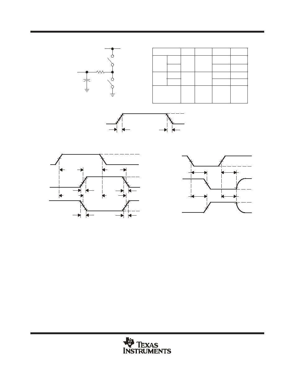
PARAMETER MEASUREMENT INFORMATION
From Output
Under Test
RL
VCC
S1
S2
LOAD CIRCUIT
PARAMETER
CL
tPZH
tpd or tt
tdis
ten
tPZL
tPHZ
tPLZ
1 k
1 k
50 pF
or
150 pF
50 pF
Open
Closed
RL
S1
Closed
Open
S2
Open
Closed
Closed
Open
50 pF
or
150 pF
Open
Open
≠≠
NOTES: A. CL includes probe and test-fixture capacitance.
B. Waveform 1 is for an output with internal conditions such that the output is low except when disabled by the output control.
Waveform 2 is for an output with internal conditions such that the output is high except when disabled by the output control.
C. Phase relationships between waveforms were chosen arbitrarily. All input pulses are supplied by generators having the following
characteristics: PRR
1 MHz, ZO = 50
, tr = 6 ns, tf = 6 ns.
D. The outputs are measured one at a time with one input transition per measurement.
E. tPLZ and tPHZ are the same as tdis.
F. tPZL and tPZH are the same as ten.
G. tPLH and tPHL are the same as tpd.
CL
(see Note A)
Test
Point
VOLTAGE WAVEFORM
INPUT RISE AND FALL TIMES
1.3 V
1.3 V
0.3 V
0.3 V
2.7 V
2.7 V
3 V
0 V
tr
tf
Input
VOLTAGE WAVEFORMS
PROPAGATION DELAY AND OUTPUT RISE AND FALL TIMES
1.3 V
1.3 V
1.3 V
10%
10%
90%
90%
3 V
VOH
VOL
0 V
tr
tf
Input
In-Phase
Output
1.3 V
tPLH
tPHL
1.3 V
1.3 V
10%
10%
90%
90%
VOH
VOL
tr
tf
tPHL
tPLH
Out-of-
Phase
Output
1.3 V
10%
90%
3 V
VCC
VOL
0 V
Output
Control
(Low-Level
Enabling)
Output
Waveform 1
(See Note B)
1.3 V
tPZL
tPLZ
VOLTAGE WAVEFORMS
ENABLE AND DISABLE TIMES FOR 3-STATE OUTPUTS
VOH
0 V
1.3 V
1.3 V
tPZH
tPHZ
Output
Waveform 2
(See Note B)
Figure 1. Load Circuit and Voltage Waveforms