Document Outline
- FEATURES
- APPLICATIONS
- DESCRIPTION
- ORDERING INFORMATION
- ABSOLUTE MAXIMUM RATINGS
- RECOMMENDED OPERATING CONDITIONS
- DISSIPATION RATING TABLE
- ELECTRICAL CHARACTERISTICS
- EQUIVALENT INPUT CIRCUIT
- PIN ASSIGNMENTS
- Terminal Functions
- PARAMETER MEASUREMENT INFORMATION
- TIMING REQUIREMENTS: 5.0V
- TIMING REQUIREMENTS: 3.0V
- TYPICAL CHARACTERISTICS
- GENERAL DESCRIPTION
- THEORY OF OPERATION
- ANALOG INPUT STAGE
- DIGITAL OUTPUT
- DIGITAL INTERFACE
- INTRODUCTION
- MODES OF OPERATION
- FILTER USAGE
- LAYOUT CONSIDERATIONS
- POWER SUPPLIES
- GROUNDING
- DECOUPLING

SBAS301A - OCTOBER 2003 - REVISED JUNE 2004
Four 1 Bit, 10MHz, 2nd Order,
Delta Sigma Modulators
ADS1204
FEATURES
D
16-Bit Resolution
D
14-Bit Linearity
D
Resolution/Speed Trade-Off:
10-Bit Effective Resolution with 10
µ
s Signal
Delay (12-Bit with 19
µ
s)
D
±
2.5V Input Range at 2.5V
D
Internal Reference Voltage: 2%
D
Gain Error: 0.5%
D
Four Independent Delta-Sigma Modulators
D
Four Input Reference Buffers
D
Onboard 20MHz Oscillator
D
Selectable Internal or External Clock
D
Operating Temperature Range:
-40
∞
C to +85
∞
C
D
QFN-32 (5x5) Package
APPLICATIONS
D
Motor Control
D
Current Measurement
D
Industrial Process Control
D
Instrumentation
D
Smart Transmitters
D
Portable Instruments
D
Weight Scales
D
Pressure Transducers
DESCRIPTION
The ADS1204 is a four-channel, high-performance device,
with four delta-sigma (
) modulators with 100dB dynamic
range, operating from a single +5V supply. The differential
inputs are ideal for direct connection to transducers in an
industrial environment. With the appropriate digital filter
and modulator rate, the device can be used to achieve
16-bit analog-to-digital (A/D) conversion with no missing
code. Effective resolution of 12 bits can be obtained with
a digital filter data rate of 160kHz at a modulator rate of
10MHz. The ADS1204 is designed for use in medium- to
high-resolution measurement applications including
current measurements, smart transmitters, industrial
process control, weight scales, chromatography, and
portable instrumentation. It is available in a QFN-32 (5x5)
package.
2nd-Order
Modulator
CH A+
AV
DD
CH A
-
Output
Interface
Circuit
RC
Oscillator
20MHz
Out
EN
Clock
Select
Divider
REFIN A
Reference
Voltage
2.5V
REFOUT
OUT A
OUT B
OUT C
OUT D
CLKIN
AGND
BGND
BV
DD
CLKOUT
CLKSEL
2nd-Order
Modulator
CH B+
CH B
-
REFIN B
2nd-Order
Modulator
CH C+
CH C
-
REFIN C
2nd-Order
Modulator
CH D+
CH D
-
REFIN D
PRODUCTION DATA information is current as of publication date. Products
conform to specifications per the terms of Texas Instruments standard warranty.
Production processing does not necessarily include testing of all parameters.
www.ti.com
Copyright
2003-2004, Texas Instruments Incorporated
Please be aware that an important notice concerning availability, standard warranty, and use in critical applications of Texas Instruments
semiconductor products and disclaimers thereto appears at the end of this data sheet.
All trademarks are the property of their respective owners.
ADS1204
SBAS301A - OCTOBER 2003 - REVISED JUNE 2004
www.ti.com
2
This integrated circuit can be damaged by ESD. Texas Instruments recommends that all integrated circuits be handled with appropriate
precautions. Failure to observe proper handling and installation procedures can cause damage.
ESD damage can range from subtle performance degradation to complete device failure. Precision integrated circuits may be more susceptible to
damage because very small parametric changes could cause the device not to meet its published specifications.
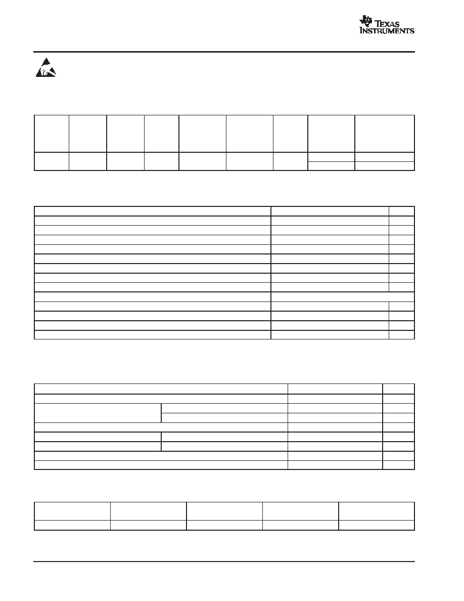
ORDERING INFORMATION
PRODUCT
MAXIMUM
INTEGRAL
LINEARITY
ERROR
(LSB)
MAXIMUM
GAIN
ERROR (%)
PACKAGE-
LEAD
PACKAGE
DESIGNATOR(1)
SPECIFIED
TEMPERATURE
RANGE
PACKAGE
MARKING
ORDERING
NUMBER
TRANSPORT MEDIA,
QUANTITY
ADS1204
±
3
±
0.5
QFN-32
RHB
-40
∞
C to +85
∞
C
ADS1204I
ADS1204IRHBT
Tape and Reel, 250
ADS1204
±
3
±
0.5
QFN-32
RHB
-40
∞
C to +85
∞
C
ADS1204I
ADS1204IRHBR
Tape and Reel, 3000
(1) For the most current specification and package information, refer to our web site at www.ti.com.
ABSOLUTE MAXIMUM RATINGS
over operating free-air temperature range unless otherwise noted(1)
ADS1204
UNIT
Supply Voltage, AVDD to AGND
-0.3 to 6
V
Supply Voltage, BVDD to BGND
-0.3 to 6
V
Analog Input Voltage with Respect to AGND
AGND - 0.3 to AVDD + 0.3
V
Reference Input Voltage with Respect to AGND
AGND - 0.3 to AVDD + 0.3
V
Digital Input Voltage with Respect to BGND
BGND - 0.3 to BVDD + 0.3
V
Ground Voltage Difference, AGND to BGND
±
0.3
V
Voltage Differences, BVDD to AGND
-0.3 to 6
V
Input Current to Any Pin Except Supply
±
10
mA
Power Dissipation
See Dissipation Rating Table
Operating Virtual Junction Temperature Range, TJ
-40 to +150
∞
C
Operating Free-Air Temperature Range, TA
-40 to +85
∞
C
Storage Temperature Range, TSTG
-65 to +150
∞
C
Lead Temperature (1.6mm or 1/16
from case for 10s)
260
∞
C
(1) Stresses beyond those listed under Absolute Maximum Ratings may cause permanent damage to the device. These are stress ratings only, and
functional operation of the device at these or any other conditions beyond those indicated under Recommended Operating Conditions is not
implied. Exposure to absolute-maximum-rated conditions for extended periods may affect device reliability.
RECOMMENDED OPERATING CONDITIONS
PARAMETER
MIN
NOM
MAX
UNIT
Supply Voltage, AVDD to AGND
4.75
5
5.25
V
Supply Voltage, BVDD to BGND
Low-Voltage Levels
2.7
3.6
V
Supply Voltage, BVDD to BGND
5V Logic Levels
4.5
5
5.5
V
Reference Input Voltage
0.5
2.5
2.6
V
Operating Common-Mode Signal
0
AVDD
V
Analog Inputs
+IN - (-IN)
0
±
REFIN
V
External Clock(1)
16
20
24
MHz
Operating Junction Temperature Range, TJ
-40
105
∞
C
(1) With reduced accuracy, clock can go from 1MHz up to 32MHz; see Typical Characteristic curves.
DISSIPATION RATING TABLE
PACKAGE
TA
25
∞
C
POWER RATING
DERATING FACTOR
ABOVE TA = 25
∞
C(1)
TA = 70
∞
C
POWER RATING
TA = 85
∞
C
POWER RATING
QFN-32 (5x5)
2725mW
27.25mW/
∞
C
1499mW
1090mW
(1) This is the inverse of the traditional junction-to-ambient thermal resistance (R
q
JA). Thermal resistances are not production tested and are for
informational purposes only.

ADS1204
SBAS301A - OCTOBER 2003 - REVISED JUNE 2004
www.ti.com
3
ELECTRICAL CHARACTERISTICS
Over recommended operating free-air temperature range at -40
∞
C to +85
∞
C, AVDD = 5V, BVDD = 3V, CH x+ = 0.5V to 4.5V, CH x- = 2.5V,
REFIN = REFOUT = internal +2.5V, CLKIN = 20MHz, and 16-bit Sinc3 filter with decimation by 256, unless otherwise noted.
ADS1204I
PARAMETER
TEST CONDITIONS
MIN
TYP(1)
MAX
UNITS
Resolution
16
Bits
DC Accuracy
INL
Integral linearity error(2)
±
1
±
3
LSB
INL
Integral linearity error(2)
±
0.001
±
0.005
% FSR
Integral linearity match
6
LSB
Integral linearity match
0.009
% FSR
DNL
Differential nonlinearity(3)
±
1
LSB
VOS
Input offset error
-1.4
±
3
mV
Input offset error match
2
mV
TCVOS
Input offset error drift
2
8
µ
V/
∞
C
GERR
Gain error(4)
Referenced to VREF
0.08
±
0.5
% FSR
Gain error match
0.185
0.5
% FSR
TCGERR
Gain error drift
2
ppm/
∞
C
PSRR
Power-supply rejection ratio
4.75V < AVDD < 5.25V
78
dB
Analog Input
FSR
Full-scale differential range
(CH x+) - (CH x-); CH x- = 2.5V
±
2.5
V
Specified differential range
(CH x+) - (CH x-); CH x- = 2.5V
±
2
V
Maximum operating input range(3)
0
AVDD
V
Input capacitance
Common-mode
3
pF
Input leakage current
CLK turned off
±
1
nA
Differential input resistance
100
k
Differential input capacitance
2.5
pF
CMRR
Common-mode rejection ratio
At DC
100
dB
CMRR
Common-mode rejection ratio
VIN =
±
1.25VPP at 40kHz
110
dB
BW
Bandwidth
FS sine wave, -3dB
50
MHz
Sampling Dynamics
Internal clock frequency
CLKSEL = 1
8
10
12
MHz
CLKIN
External clock frequency
CLKSEL = 0
1
20
24
MHz
AC Accuracy
THD
Total harmonic distortion
VIN =
±
2VPP at 5kHz
-96
-88
dB
SFDR
Spurious-free dynamic range
VIN =
±
2VPP at 5kHz
92
100
dB
SNR
Signal-to-noise ratio
VIN =
±
2VPP at 5kHz
86
89
dB
SINAD
Signal-to-noise + distortion
VIN =
±
2VPP at 5kHz
85
89
dB
Channel-to-channel isolation(3)
VIN =
±
2VPP at 50kHz
85
dB
ENOB
Effective number of bits
14
14.5
Bits
(1) All typical values are at TA = +25
∞
C.
(2) Integral nonlinearity is defined as the maximum deviation of the line through the end points of the specified input range of the transfer curve
for CH x+ = -2V to +2V at 2.5V, expressed either as the number of LSBs or as a percent of measured input range (4V).
(3) Ensured by design.
(4) Maximum values, including temperature drift, are ensured over the full specified temperature range.
(5) Applicable for 5.0V nominal supply: BVDD (min) = 4.5V and BVDD (max) = 5.5V.
(6) Applicable for 3.0V nominal supply: BVDD (min) = 2.7V and BVDD (max) = 3.6V.

ADS1204
SBAS301A - OCTOBER 2003 - REVISED JUNE 2004
www.ti.com
4
ELECTRICAL CHARACTERISTICS (continued)
Over recommended operating free-air temperature range at -40
∞
C to +85
∞
C, AVDD = 5V, BVDD = 3V, CH x+ = 0.5V to 4.5V, CH x- = 2.5V,
REFIN = REFOUT = internal +2.5V, CLKIN = 20MHz, and 16-bit Sinc3 filter with decimation by 256, unless otherwise noted.
PARAMETER
UNITS
ADS1204I
TEST CONDITIONS
PARAMETER
UNITS
MAX
TYP(1)
MIN
TEST CONDITIONS
Voltage Reference Output
VOUT
Reference voltage output
-40
∞
C to +85
∞
C
2.450
2.5
2.550
V
dVOUT/dT
Output voltage temperature drift
±
20
ppm/
∞
C
Output voltage noise
f = 0.1Hz to 10Hz, CL = 10
µ
F
10
µ
Vrms
Output voltage noise
f =10Hz to 10kHz, CL = 10
µ
F
12
µ
Vrms
PSRR
Power-supply rejection ratio
60
dB
IOUT
Output current
10
µ
A
ISC
Short-circuit current
0.5
mA
Turn-on settling time
to 0.1% at CL = 0
100
µ
s
Voltage Reference Input
VIN
Reference voltage input
0.5
2.5
2.6
V
Reference input resistance
100
M
Reference input capacitance
5
pF
Reference input current
1
µ
A
Digital Inputs(5)
Logic family
CMOS with Schmitt Trigger
VIH
High-level input voltage
0.7
◊
BVDD
BVDD+0.3
V
VIL
Low-level input voltage
-0.3
0.3
◊
BVDD
V
IIN
Input current
VI = BVDD or GND
±
50
nA
CI
Input capacitance
5
pF
Digital Outputs(5)
Logic family
CMOS
VOH
High-level output voltage
BVDD = 4.5V, IOH = -100
µ
A
4.44
V
VOL
Low-level output voltage
BVDD = 4.5V, IOL = +100
µ
A
0.5
V
CO
Output capacitance
5
pF
CL
Load capacitance
30
pF
Data format
Bit Stream
(1) All typical values are at TA = +25
∞
C.
(2) Integral nonlinearity is defined as the maximum deviation of the line through the end points of the specified input range of the transfer curve
for CH x+ = -2V to +2V at 2.5V, expressed either as the number of LSBs or as a percent of measured input range (4V).
(3) Ensured by design.
(4) Maximum values, including temperature drift, are ensured over the full specified temperature range.
(5) Applicable for 5.0V nominal supply: BVDD (min) = 4.5V and BVDD (max) = 5.5V.
(6) Applicable for 3.0V nominal supply: BVDD (min) = 2.7V and BVDD (max) = 3.6V.

ADS1204
SBAS301A - OCTOBER 2003 - REVISED JUNE 2004
www.ti.com
5
ELECTRICAL CHARACTERISTICS (continued)
Over recommended operating free-air temperature range at -40
∞
C to +85
∞
C, AVDD = 5V, BVDD = 3V, CH x+ = 0.5V to 4.5V, CH x- = 2.5V,
REFIN = REFOUT = internal +2.5V, CLKIN = 20MHz, and 16-bit Sinc3 filter with decimation by 256, unless otherwise noted.
PARAMETER
UNITS
ADS1204I
TEST CONDITIONS
PARAMETER
UNITS
MAX
TYP(1)
MIN
TEST CONDITIONS
Digital Inputs(6)
Logic family
LVCMOS
VIH
High-level input Voltage
BVDD = 3.6V
2
BVDD+0.3
V
VIL
Low-level input voltage
BVDD = 2.7V
-0.3
0.8
V
IIN
Input current
VI = BVDD or GND
±
50
nA
CI
Input capacitance
5
pF
Digital Outputs(6)
Logic family
LVCMOS
VOH
High-level output voltage
BVDD = 2.7V, IOH = -100
µ
A
BVDD-0.2
V
VOL
Low-level output voltage
BVDD = 2.7V, IOL = +100
µ
A
0.2
V
CO
Output capacitance
5
pF
CL
Load capacitance
30
pF
Data format
Bit Stream
Power Supply
AVDD
Analog supply voltage
4.5
5.5
V
BVDD
Buffer I/O supply voltage
Low-voltage levels
2.7
3.6
V
BVDD
Buffer I/O supply voltage
5V logic levels
4.5
5.5
V
AIDD
Analog operating supply current
CLKSEL = 1
22.5
30
mA
AIDD
Analog operating supply current
CLKSEL = 0
22.4
29
mA
BIDD
Buffer I/O operating supply current
BVDD = 3V, CLKOUT = 10MHz
4
mA
BIDD
Buffer I/O operating supply current
BVDD = 5V, CLKOUT = 10MHz
4
mA
Power dissipation
CLKSEL = 0
122
145
mW
Power dissipation
CLKSEL = 1
112.5
150
mW
(1) All typical values are at TA = +25
∞
C.
(2) Integral nonlinearity is defined as the maximum deviation of the line through the end points of the specified input range of the transfer curve
for CH x+ = -2V to +2V at 2.5V, expressed either as the number of LSBs or as a percent of measured input range (4V).
(3) Ensured by design.
(4) Maximum values, including temperature drift, are ensured over the full specified temperature range.
(5) Applicable for 5.0V nominal supply: BVDD (min) = 4.5V and BVDD (max) = 5.5V.
(6) Applicable for 3.0V nominal supply: BVDD (min) = 2.7V and BVDD (max) = 3.6V.
EQUIVALENT INPUT CIRCUIT
R
ON
650
C
(SAMPLE)
1pF
BV
DD
D
IN
BGND
AV
DD
A
IN
AGND
Diode Turn-On Voltage: 0.35V
Equivalent Digital Input Circuit
Equivalent Analog Input Circuit