 | –≠–ª–µ–∫—Ç—Ä–æ–Ω–Ω—ã–π –∫–æ–º–ø–æ–Ω–µ–Ω—Ç: ADS5121 | –°–∫–∞—á–∞—Ç—å:  PDF PDF  ZIP ZIP |
Document Outline
- FEATURES
- APPLICATIONS
- DESCRIPTION
- ABSOLUTE MAXIMUM RATINGS
- PACKAGE/ORDERING INFORMATION
- BLOCK DIAGRAM
- DC CHARACTERISTICS
- AC CHARACTERISTICS
- SWITCHING CHARACTERISTICS
- TIMING DIAGRAM (Per ADC Channel)
- PIN DESCRIPTIONS
- PIN CONFIGURATION
- DATA OUTPUT PINS
- TYPICAL CHARACTERISTICS
- APPLICATION INFORMATION
- CONVERTER OPERATION
- INPUT IMPEDANCE
- INPUT BIASING
- DRIVING THE ANALOG INPUTS
- Differential versus Single-Ended
- INPUT DRIVER CONFIGURATIONS
- Transformer-Coupled Interface
- Single-Ended, AC-Coupled Driver
- DC-Coupled Interface with Differential Amplifier
- REFERENCE OPERATION
- INTERNAL REFERENCE
- USING EXTERNAL REFERENCES
- DIGITAL INPUTS AND OUTPUTS
- MINIMUM SAMPLING RATE
- DATA OUTPUT FORMAT
- DIGITAL OUTPUT LOADING
- OUTPUT ENABLE
- POWER-DOWN (STANDBY)
- DIGITAL OUTPUT DRIVER SUPPLY, DRV DD
- GROUNDING AND DECOUPLING
- LAYOUT OF THE PCB WITH A MICROSTAR BGA PACKAGE
- TERMINOLOGY
- ANALOG BANDWIDTH
- APERTURE DELAY
- APERTURE UNCERTAINTY (JITTER)
- EFFECTIVE NUMBER OF BITS (ENOB)
- EFFECTIVE RESOLUTION BANDWIDTH
- GAIN ERROR
- GAIN MATCHING
- 2ND-HARMONIC DISTORTION
- 3RD-HARMONIC DISTORTION
- INTERMODULATION DISTORTION (IMD)
- OFFSET ERROR (ZERO-SCALE ERROR)
- OFFSET MATCHING
- POWER-SUPPLY REJECTION RATIO (PSRR)
- SIGNAL-TO-NOISE AND DISTORTION (SINAD)
- SIGNAL-TO-NOISE RATIO (WITHOUT HARMONICS)
- SPURIOUS-FREE DYNAMIC RANGE (SFDR)
- PACKAGE DRAWING
ADS5121
SBAS281 ≠ MAY 2003
www.ti.com
DESCRIPTION
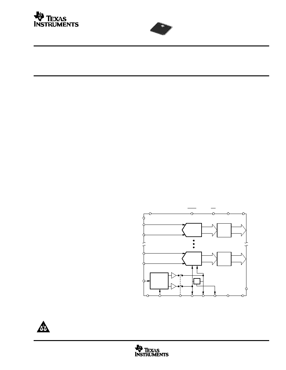
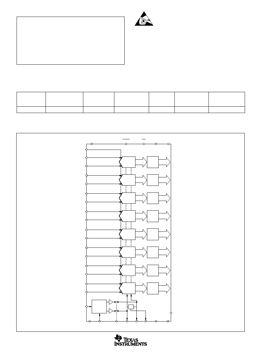
The ADS5121 is a low-power, 8-channel, 10-bit, 40MSPS
CMOS Analog-to-Digital Converter (ADC) that operates from
a single 1.8V supply, while offering 1.8V and 3.3V digital I/O
flexibility. A single-ended input clock is used for simultaneous
sampling of up to eight analog differential input channels. The
flexible duty cycle adjust circuit (DCASEL) allows the use of a
non-50% clock duty cycle. Individual standby pins allow users
the ability to power-down any number of ADCs.
The internal reference can be bypassed to use an external
reference to suit the accuracy and temperature drift require-
ments of the application. A 10-bit parallel bus on eight chan-
nels is provided with 3-state outputs.
The speed, resolution, and low power of the ADS5121 make
it ideal for applications requiring high-density signal process-
ing in low-power environments.
The ADS5121 is characterized for operation from ≠40
∞
C to
+85
∞
C.
FEATURES
q
8 DIFFERENTIAL ANALOG INPUTS
q
1V
PP
DIFFERENTIAL INPUT RANGE
q
INT/EXT VOLTAGE REFERENCE
q
ANALOG/DIGITAL SUPPLY: 1.8V
q
DIGITAL I/O SUPPLY: 1.8V/3.3V
q
DIFFERENTIAL NONLINEARITY:
±
0.4LSB
q
INTEGRAL NONLINEARITY:
±
0.6LSB
q
SIGNAL-TO-NOISE: 60dB at f
IN
= 20MHz
q
POWER DISSIPATION: 500mW
q
INDIVIDUAL CHANNEL POWER-DOWN
q
257-LEAD, 0.8 BALL PITCH, PLASTIC
MicroSTAR BGATM (16mm ∑ 16mm)
Copyright © 2003, Texas Instruments Incorporated
8-Channel, 10-Bit, 40MSPS, 1.8V
CMOS ANALOG-TO-DIGITAL CONVERTER
MicroSTAR BGA is a trademark of Texas Instruments. All other trademarks are the property of their respective owners.
Please be aware that an important notice concerning availability, standard warranty, and use in critical applications of
Texas Instruments semiconductor products and disclaimers thereto appears at the end of this data sheet.
10-Bit
ADC
3-State
Output
Buffers
D[9:0]
A
10-Bit
ADC
3-State
Output
Buffers
D[9:0]
H
DCASEL
AINA+
CLK
AINA≠
AINH≠
AINH+
IREFR
AV
DD
STBY
OE
DRV
DD
DV
DD
Internal
Reference
Circuit
CM
AGND
DRVGND DGND
BG
PDREF REFT REFB
CML
APPLICATIONS
q
PORTABLE ULTRASOUND
q
PORTABLE INSTRUMENTATION
PRODUCTION DATA information is current as of publication date.
Products conform to specifications per the terms of Texas Instruments
standard warranty. Production processing does not necessarily include
testing of all parameters.
ADS
5121
ADS5121
2
SBAS281
www.ti.com
ABSOLUTE MAXIMUM RATINGS
(1)
Supply Voltage: AV
DD
to AGND, DV
DD
to DGND ............. ≠0.3V to +2.2V
DRV
DD
to DRGND ................................... ≠0.3V to +4.0V
AGND
to DGND ...................................... ≠0.3V to +0.3V
AV
DD
to DV
DD
.......................................... ≠2.2V to +2.2V
Reference Voltage Input Range REFT, REFB to AGND ... ≠0.3V to AV
DD
+ 0.3V
Analog Input Voltage Range AIN to AGND ........... ≠0.3V to AV
DD
+ 0.3V
Clock Input CLK to DGND ..................................... ≠0.3V to AV
DD
+ 0.3V
Digital Input to DGND ........................................... ≠0.3V to DV
DD
+ 0.3V
Digital Outputs to DRGND .................................. ≠0.3V to DRV
DD
+ 0.3V
Operating Temperature Range (T
J
) ................................... 0
∞
C to +105
∞
C
Storage Temperature Range (T
STG
) ................................. ≠65
∞
C + 150
∞
C
NOTE: (1) Stresses above those listed under "Absolute Maximum Ratings"
may cause permanent damage to the device. Exposure to absolute maximum
conditions for extended periods may affect device reliability.
ELECTROSTATIC
DISCHARGE SENSITIVITY
This integrated circuit can be damaged by ESD. Texas Instru-
ments recommends that all integrated circuits be handled with
appropriate precautions. Failure to observe proper handling
and installation procedures can cause damage.
ESD damage can range from subtle performance degradation
to complete device failure. Precision integrated circuits may be
more susceptible to damage because very small parametric
changes could cause the device not to meet its published
specifications.
STBY
10-Bit
ADC
3-State
Output
Buffers
D[9:0]
A
10-Bit
ADC
3-State
Output
Buffers
D[9:0]
B
10-Bit
ADC
3-State
Output
Buffers
D[9:0]
C
10-Bit
ADC
3-State
Output
Buffers
D[9:0]
D
10-Bit
ADC
3-State
Output
Buffers
D[9:0]
E
10-Bit
ADC
3-State
Output
Buffers
D[9:0]
F
10-Bit
ADC
3-State
Output
Buffers
D[9:0]
G
10-Bit
ADC
3-State
Output
Buffers
D[9:0]
H
DCASEL
AINA+
CLK
AINA≠
AINB≠
AINB+
AINC+
AINC≠
AIND≠
AIND+
AINE+
AINE≠
AINF≠
AINF+
AING+
AING≠
AINH≠
AINH+
IREFR
AV
DD
OE
DRV
DD
DV
DD
Internal
Reference
Circuit
CM
AGND
DRVGND DGND
BG
PDREF REFT
REFB CML
BLOCK DIAGRAM
SPECIFIED
PACKAGE
TEMPERATURE
PACKAGE
ORDERING
TRANSPORT
PRODUCT
PACKAGE-LEAD
DESIGNATOR
(1)
RANGE
MARKING
NUMBER
MEDIA, QUANTITY
ADS5121
MicroSTAR BGA-257
GHK
≠40
∞
C to +85
∞
C
ADS5121IGHK
ADS5121IGHK
Tray, 90
NOTE: (1) For the most current specifications and package information, refer to our web site at www.ti.com.
PACKAGE/ORDERING INFORMATION
ADS5121
3
SBAS281
www.ti.com
ADS5121
DC CHARACTERISTICS
AV
DD
= DV
DD
= 1.8V, DRV
DD
= 3.3V, Clock = 40MSPS, 50% Clock Duty Cycle, ≠0.5dBFS Input Span, Internal Reference, I
REFR
= 6.8k
, T
MIN
= ≠40
∞
C, T
MAX
= +85
∞
C,
and typical values at T
A
= 25
∞
C, unless otherwise noted.
PARAMETER
CONDITION
MIN
TYP
MAX
UNITS
RESOLUTION
10
Bits
DC ACCURACY
Differential Nonlinearity, DNL
≠0.9
±
0.4
+1.0
LSB
Integral Nonlinearity, INL
≠1.5
±
0.6
+1.5
LSB
No Missing Codes
Tested
Gain Error
External Reference
≠0.6
0.1
+0.6
%FSR
Offset Error
External Reference
0.2
+1.8
%FSR
Gain Temperature Coefficient
6.0
ppm/
∞
C
Gain Matching
±
0.4
%FSR
ANALOG INPUT
Input Voltage Range (AIN+, AIN≠)
REFB
REFT
V
Input Voltage, Differential Full-Scale
1
V
PP
Input Common-Mode Range
(REFT + REFB) / 2
V
Input Resistance, R
IN
f
CLK
= 40MSPS
83
k
Input Capacitance, C
IN
5
pF
INTERNAL REFERENCE VOLTAGES
Reference, Top (REFT)
1.30
1.34
1.42
V
Reference, Bottom (REFB)
0.76
0.82
0.87
V
Int Reference Temperature Coefficient
10
ppm/
∞
C
EXTERNAL REFERENCE GENERATION
Reference, Top (REFT)
1.15
1.25
1.35
V
Reference, Bottom (REFB)
0.65
0.75
0.85
V
Input Resistance, REFR
IN
(between REFB and REFT)
80
POWER SUPPLY
f
IN
= 3.5MHz
Operating Supply Current, I
DD
242
255
mA
Analog Operating Supply Current, IAV
DD
155
170
mA
Digital Operating Supply Current, IDV
DD
43
48
mA
Driver Operating Supply Current, IDRV
DD
C
L
= 20pF, 3.3V
42
48
mA
C
L
= 20pF, 1.8V
22
30
mA
Operating Voltage
AV
DD
1.65
1.8
2.0
V
DV
DD
1.65
1.8
2.0
V
DRV
DD
1.65
1.8
3.6
V
Power-Dissipation
DRV
DD
= 3.3V
500
525
mW
DRV
DD
= 1.8V
404
420
mW
Power Standby
CLK Running
62
70
mW
CLK Stopped
52
60
mW
PDREF = 1, External REF, CLK Running
12
15
mW
PDREF = 1, External REF, CLK Stopped
1.6
5
mW
Power-Supply Rejection Ratio, PSRR
±
5%, AV
DD
2
mV/V
ADS5121
DC CHARACTERISTICS
AV
DD
= DV
DD
= 1.8V, DRV
DD
= 3.3V, Clock = 40MSPS, 50% Clock Duty Cycle, ≠0.5dBFS Input Span, Internal Reference, and T
MIN
to T
MAX
, unless otherwise noted.
PARAMETER
CONDITION
MIN
TYP
MAX
UNITS
DIGITAL INPUTS (STBY A-H, PDREF, OE)
DRV
DD
= 3.3V/1.8V
High-Level Input Voltage, V
IH
V
IH
= DRV
DD
0.70 ∑ DRV
DD
V
Low-Level Input Voltage, V
IL
V
IL
= 0V
0.25 ∑ DRV
DD
V
High-Level Input Current, I
IH
±
1
µ
A
Low-Level Input Current, I
IL
±
1
µ
A
DIGITAL INPUTS (DCASEL)
High-Level Input Voltage, V
IH
V
IH
= DV
DD
0.70 ∑ DV
DD
V
Low-Level Input Voltage, V
IL
V
IL
= 0V
0.25 ∑ DV
DD
V
High-Level Input Current, I
IH
±
1
µ
A
Low-Level Input Current, I
IL
±
1
µ
A
DIGITAL OUTPUTS ( DRV
DD
= 3.3/1.8V)
High-Level Output Voltage, V
OH
I
OH
= ≠50
µ
A
0.8 ∑ DRV
DD
V
Low-Level Output Voltage, V
OL
I
OL
= 50
µ
A
0.2 ∑ DRV
DD
V
External Load Capacitance, C
L
15
pF
3-State Leakage Current, I
LEAK
OE = HIGH
±
1
µ
A
ADS5121
4
SBAS281
www.ti.com
ADS5121
AC CHARACTERISTICS
AV
DD
= DV
DD
= 1.8V, DRV
DD
= 3.3V, 50% Clock Duty Cycle, CLK = 40MSPS, Analog Input at ≠0.5dBFS Input Span, Internal Voltage Reference, I
REFR
= 6.8k
,
T
MIN
= ≠40
∞
C, T
MAX
= +85
∞
C, and typical values at T
A
= 25
∞
C, unless otherwise noted.
ADS5121
SWITCHING CHARACTERISTICS
AV
DD
= DV
DD
= 1.8V, DRV
DD
= 3.3V, 50% Clock Duty Cycle, CLK = 40MSPS, Analog Input at ≠0.5dBFS Input Span, Internal Voltage Reference, T
MIN
= ≠40
∞
C,
T
MAX
= +85
∞
C, and typical values at T
A
= 25
∞
C.
PARAMETER
CONDITION
MIN
TYP
MAX
UNITS
Maximum Conversion Rate
5
40
MSPS
Clock Duty Cycle
DCASEL Enabled
30 to 70
%
Data Latency
(1)
6.5
Clk Cycles
Clock
to Data Valid
t
DO
(1)
8
10
ns
OE
to Outputs Enabled
t
EN
(1)
8
ns
OE
Rising to Outputs Tri-Stated
t
DIS
8
ns
Aperture Delay
1
ns
Aperture Uncertainty (Jitter)
2
ps, r ms
NOTE: (1) See timing diagram.
PARAMETER
CONDITION
MIN
TYP
MAX
UNITS
Signal-to-Noise Ratio
(SNR)
f
IN
= 3.5MHz
56
60
dB
f
IN
= 10MHz
56
60
dB
f
IN
= 20MHz
60
dB
Signal-to-Noise and Distortion
(SINAD)
f
IN
= 3.5MHz
56
59
dB
f
IN
= 10MHz
56
59
dB
f
IN
= 20MHz
59
dB
Effective Number of Bits
(ENOB)
f
IN
= 3.5MHz
9.0
9.5
Bits
f
IN
= 10MHz
9.0
9.5
Bits
f
IN
= 20MHz
9.5
Bits
Spurious-Free Dynamic Range
(SFDR)
f
IN
= 3.5MHz
66
75
dBc
f
IN
= 10MHz
65
74
dBc
f
IN
= 20MHz
73
dBc
2nd-Harmonic Distortion
(HD2)
f
IN
= 3.5MHz
69
85
dBc
f
IN
= 10MHz
68
85
dBc
f
IN
= 20MHz
84
dBc
3rd-Harmonic Distortion
(HD3)
f
IN
= 3.5MHz
66
77
dBc
f
IN
= 10MHz
65
75
dBc
f
IN
= 20MHz
73
dBc
2-Tone Intermodulation Distortion
(IMD)
f
1
= 4.43MHz, f
2
= 4.53MHz at ≠6.5dB
≠69
dBFS
Channel-to-Channel Crosstalk
f
IN
= 10MHz, DRV
DD
= 3.3V
89
dB
Effective Resolution Bandwidth
22
MHz
Over-Voltage Recovery Time
(1)
20
ns
Differential Gain
(1)
±
1
%
Differential Phase
(1)
±
0.25
Degrees
NOTE: (1) Assured by design.
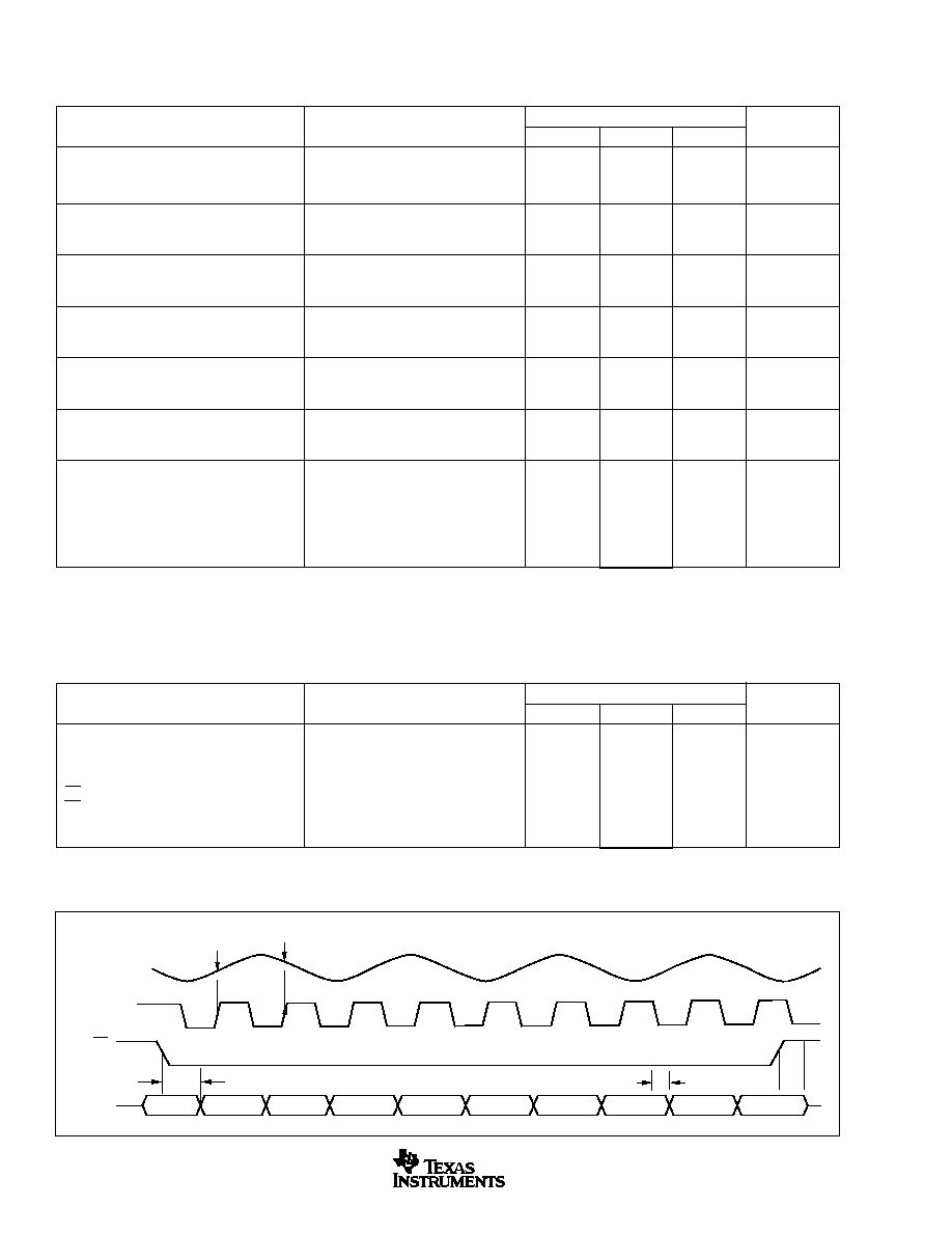
TIMING DIAGRAM (Per ADC Channel)
Analog
Input
CLK
OE
D[9:0]
S ≠ 5
S ≠ 6
S ≠ 4
S ≠ 3
S ≠ 2
S ≠ 1
S1
S2
S3
t
DO
t
DIS
t
EN
Sample 1
Sample 2
8
9
7
6
5
4
3
2
1
ADS5121
5
SBAS281
www.ti.com
NAME
PINS
I/O
TERMINAL DESCRIPTION
AV
DD
C6, C7, E6, F1, F2, F3, F5, F6, J6, N3, P3, P5, P6, P7, R6, V6, W6
I
Analog Supply (1.8V)
AGND
A3, A5, B5, B9, C1, C5, C9, E3, E7, F7, G1, G5, G6, H6, J1, J2, M2, N5, N6, P8,
I
Analog Ground
R1, R2, R3, R7, U1, U5, U10, V5, V10, W3, W7
AINA+
U7
I
Analog Input Channel A
AINA≠
V7
I
Complementary Analog Input Channel A
AINB+
W4
I
Analog Input Channel B
AINB≠
V4
I
Complementary Analog Input Channel B
AINC+
T1
I
Analog Input Channel C
AINC≠
T2
I
Complementary Analog Input Channel C
AIND+
P2
I
Analog Input Channel D
AIND≠
P1
I
Complementary Analog Input Channel D
AINE+
G3
I
Analog Input Channel E
AINE≠
G2
I
Complementary Analog Input Channel E
AINF+
D1
I
Analog Input Channel F
AINF≠
D2
I
Complementary Analog Input Channel F
AING+
A4
I
Analog Input Channel G
AING≠
B4
I
Complementary Analog Input Channel G
AINH+
B6
Analog Input Channel H
AINH≠
A6
I
Complementary Analog Input Channel H
CLK
W9
I
Clock Input
REFT
K3, L1, J3
I/O
Reference Top
REFB
K5, J5, L5
I/O
Reference Bottom
CML
L2, L3
O
Common-Mode Level Output
BG
K1
I/O
Bandgap Decoupling (Decouple with 0.1
µ
F cap to AGND)
IREFR
K6
I
Internal Reference Bias Current (Connect 6.8k
resistor
from this pin AGND to set internal bias amplifier current.)
DNC
L6
I
Do Not Connect
DNC
M1
I
Do Not Connect
NC
E1, E2, E5, K2, U6, W5
I
No Internal Connection
DCASEL
N2
I
Duty Cycle Adjust
DV
DD
C2, C3, C4, D3, E8, F8, H3, H5, M3, M5, R8, T3, U3, U4, U8, V3, P13, R13
I
Digital Supply (1.8V)
P17, L15, J14, F17, F12, E12
DGND
A2, A7, B1, B2, B3, B7, B13, C13, G15, H1, H2, H17, L17, M6, N1, N15, U2, U13,
I
Digital Ground
U14, V1, V2, V8, W2, W8
PDREF
V9
I
Power-Down Ref: 0 = internal reference, 1 = external
reference. In external reference mode connect REFT to
BG pin.
STBY A
W10
I
Power-Down Channel A
STBY B
P9
I
Power-Down Channel B
STBY C
R9
I
Power-Down Channel C
STBY D
U9
I
Power-Down Channel D
STBY E
C8
I
Power-Down Channel E
STBY F
B8
I
Power-Down Channel F
STBY G
A8
I
Power-Down Channel G
STBY H
A9
I
Power-Down Channel H
OE
P10
I
Enable all Digital Outputs, Ch. A-H. OE: 0 = Outputs
Enable. OE: 1 = Outputs disabled (3-state).
DRV
DD
B17, C16, D17, E9, E10, E11, E17, F9, H14, H15, K17, L14, N14, P12, P14, P15
I
Driver Digital Supply (1.8V or 3.3V)
R10, R12, R14
I
DRGND
E13, F10, F11, F13, F14, F15, G14, G17, M14, M15, M17, N17, U11, U12, U15, U16
I
Driver Digital Ground
PIN DESCRIPTIONS
19
14,40 TYP
17
16
13
14
15
11
12
9
8
10
V
U
W
R
N
P
L
M
K
T
7
5
6
3
4
H
F
G
E
C
D
1
A
B
2
J
18
0,80
0,80
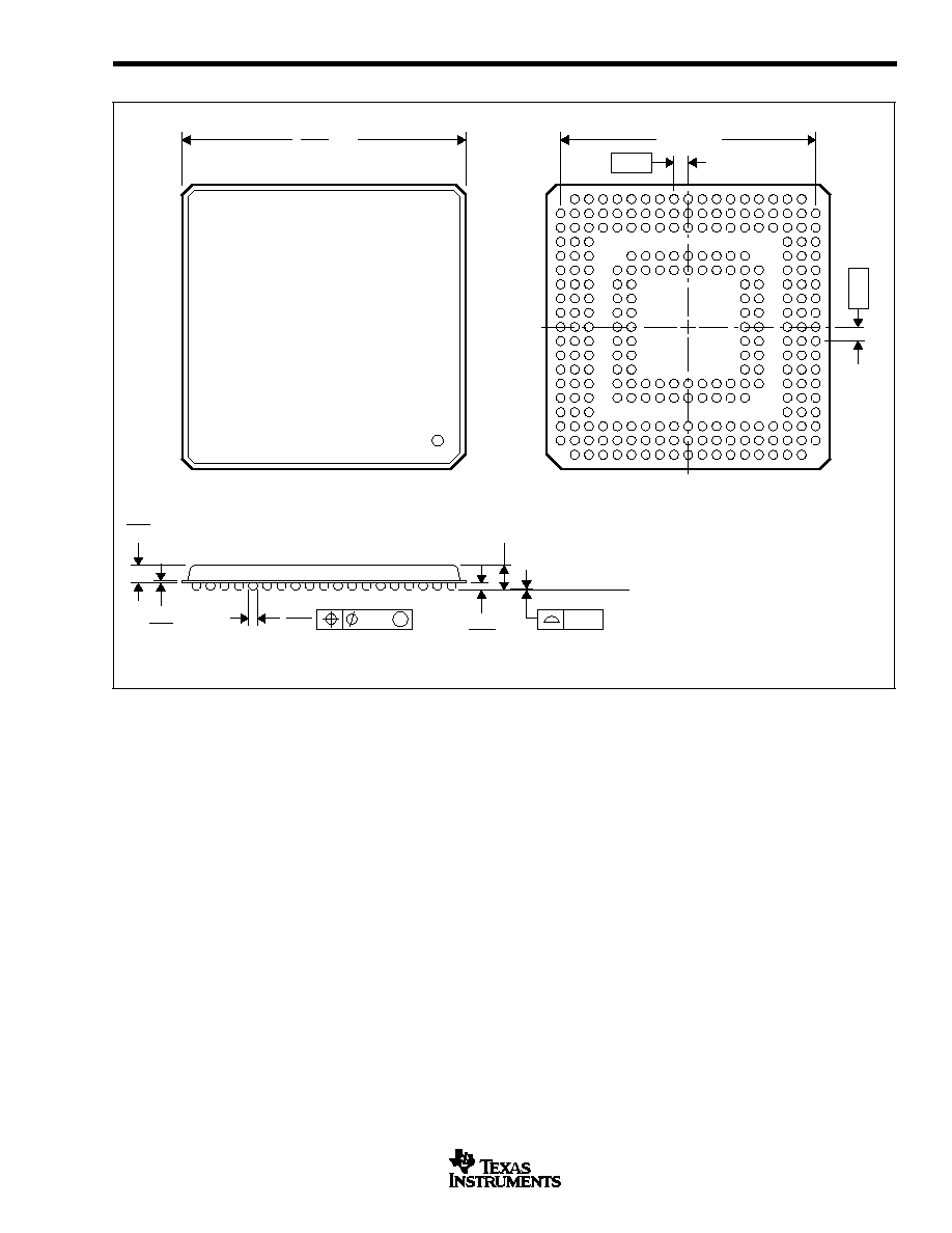
PIN CONFIGURATION
Bottom View
BGA
ADS5121
6
SBAS281
www.ti.com
NAME
PINS
I/O
TERMINAL DESCRIPTION
D0A
V14
O
Bit 1, Channel A (LSB)
D1A
W14
O
Bit 2, Channel A
D2A
V13
O
Bit 3, Channel A
D3A
W13
O
Bit 4, Channel A
D4A
V12
O
Bit 5, Channel A
D5A
W12
O
Bit 6, Channel A
D6A
R11
O
Bit 7, Channel A
D7A
P11
O
Bit 8, Channel A
D8A
V11
O
Bit 9, Channel A
D9A
W11
O
Bit 10, Channel A (MSB)
D0B
V19
O
Bit 1, Channel B (LSB)
D1B
V18
O
Bit 2, Channel B
D2B
U17
O
Bit 3, Channel B
D3B
W18
O
Bit 4, Channel B
D4B
V17
O
Bit 5, Channel B
D5B
W17
O
Bit 6, Channel B
D6B
V16
O
Bit 7, Channel B
D7B
W16
O
Bit 8, Channel B
D8B
V15
O
Bit 9, Channel B
D9B
W15
O
Bit 10, Channel B (MSB)
D0C
P19
O
Bit 1, Channel C (LSB)
D1C
P18
O
Bit 2, Channel C
D2C
R19
O
Bit 3, Channel C
D3C
R18
O
Bit 4, Channel C
D4C
R17
O
Bit 5, Channel C
D5C
T19
O
Bit 6, Channel C
D6C
T18
O
Bit 7, Channel C
D7C
U19
O
Bit 8, Channel C
D8C
U18
O
Bit 9, Channel C
D9C
T17
O
Bit 10, Channel C (MSB)
D0D
K14
O
Bit 1, Channel D (LSB)
D1D
K15
O
Bit 2, Channel D
D2D
K18
O
Bit 3, Channel D
D3D
K19
O
Bit 4, Channel D
D4D
L18
O
Bit 5, Channel D
D5D
L19
O
Bit 6, Channel D
D6D
M19
O
Bit 7, Channel D
D7D
M18
O
Bit 8, Channel D
D8D
N19
O
Bit 9, Channel D
D9D
N18
O
Bit 10, Channel D (MSB)
DATA OUTPUT PINS
NAME
PINS
I/O
TERMINAL DESCRIPTION
D0E
F18
O
Bit 1, Channel E (LSB)
D1E
F19
O
Bit 2, Channel E
D2E
G18
O
Bit 3, Channel E
D3E
G19
O
Bit 4, Channel E
D4E
H18
O
Bit 5, Channel E
D5E
H19
O
Bit 6, Channel E
D6E
J15
O
Bit 7, Channel E
D7E
J17
O
Bit 8, Channel E
D8E
J18
O
Bit 9, Channel E
D9E
J19
O
Bit 10, Channel E (MSB)
D0F
A18
O
Bit 1, Channel F (LSB)
D1F
B18
O
Bit 2, Channel F
D2F
C17
O
Bit 3, Channel F
D3F
B19
O
Bit 4, Channel F
D4F
C18
O
Bit 5, Channel F
D5F
C19
O
Bit 6, Channel F
D6F
D18
O
Bit 7, Channel F
D7F
D19
O
Bit 8, Channel F
D8F
E18
O
Bit 9, Channel F
D9F
E19
O
Bit 10, Channel F (MSB)
D0G
A14
O
Bit 1, Channel G (LSB)
D1G
B14
O
Bit 2, Channel G
D2G
C14
O
Bit 3, Channel G
D3G
A15
O
Bit 4, Channel G
D4G
B15
O
Bit 5, Channel G
D5G
E14
O
Bit 6, Channel G
D6G
C15
O
Bit 7, Channel G
D7G
A16
O
Bit 8, Channel G
D8G
B16
O
Bit 9, Channel G
D9G
A17
O
Bit 10, Channel G (MSB)
D0H
C10
O
Bit 1, Channel H (LSB)
D1H
B10
O
Bit 2, Channel H
D2H
A10
O
Bit 3, Channel H
D3H
C11
O
Bit 4, Channel H
D4H
B11
O
Bit 5, Channel H
D5H
A11
O
Bit 6, Channel H
D6H
A12
O
Bit 7, Channel H
D7H
B12
O
Bit 8, Channel H
D8H
C12
O
Bit 9, Channel H
D9H
A13
O
Bit 10, Channel H (MSB)
ADS5121
7
SBAS281
www.ti.com
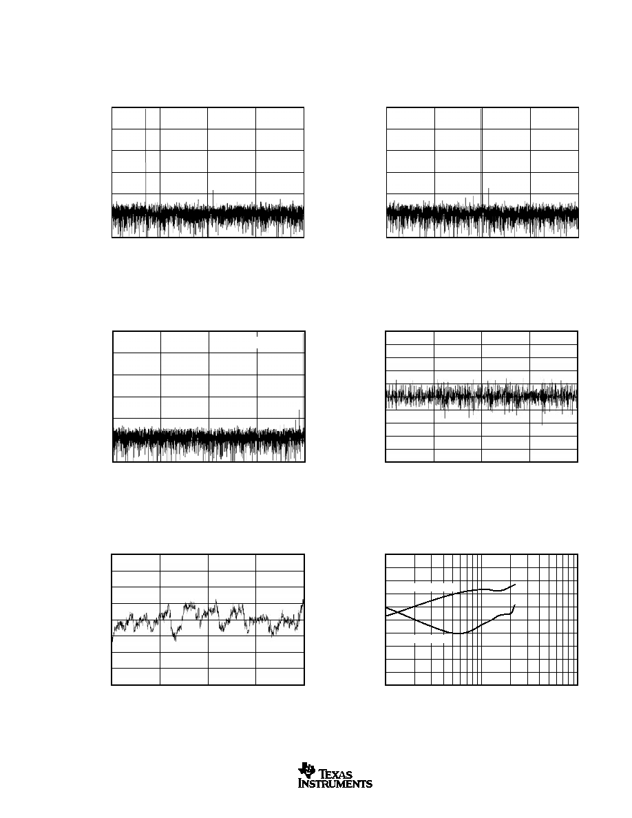
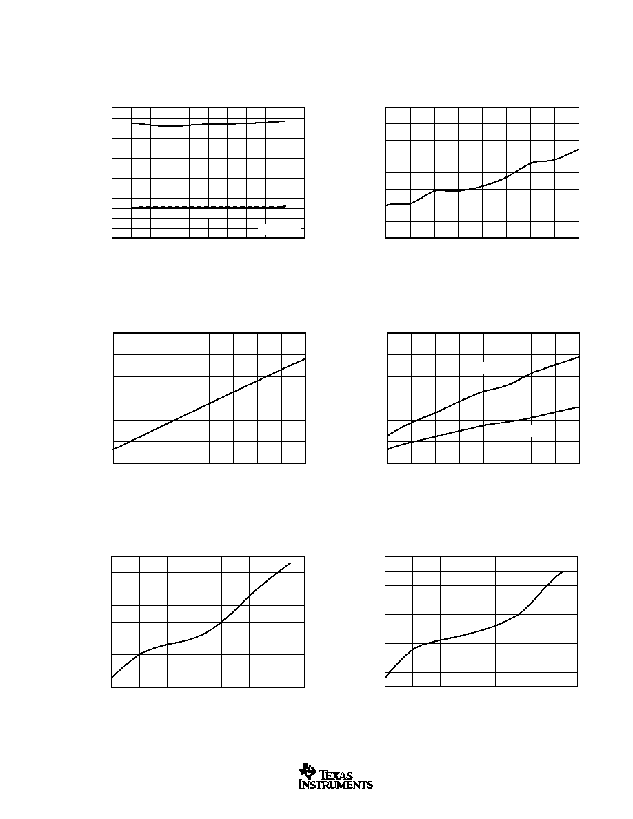
TYPICAL CHARACTERISTICS
T
A
= 25
∞
C, AV
DD
= DV
DD
= 1.8V, DRV
DD
= 3.3V, f
IN
= ≠0.5dBFS, Internal Reference, Clock = 40MSPS, and Differential Input Range = 1Vp-p, unless otherwise noted.
f
IN
= 3.5MHz
SPECTRAL PERFORMANCE
Amplitude (dB)
Frequency (Hz)
0
5
10
15
20
0
≠20
≠40
≠60
≠80
≠100
≠120
SPECTRAL PERFORMANCE
Amplitude (dB)
Frequency (Hz)
0
5
10
15
20
0
≠20
≠40
≠60
≠80
≠100
≠120
f
IN
= 9.8MHz
SPECTRAL PERFORMANCE
Amplitude (dB)
Frequency (Hz)
0
5
10
15
20
0
≠20
≠40
≠60
≠80
≠100
≠120
f
IN
= 19.8MHz
DIFFERENTIAL LINEARITY
DNL (LSB)
Input Codes
0
256
512
768
1024
1.0
0.8
0.6
0.4
0.2
0
≠0.2
≠0.4
≠0.6
≠0.8
≠1.0
INTEGRAL LINEARITY
INL (LSB)
Input Codes
0
256
512
768
1024
2.0
1.5
1.0
0.5
0
≠0.5
≠1.0
≠1.5
≠2.0
2ND- AND 3RD-HARMONIC vs INPUT FREQUENCY
Amplitude (dBc)
Input Frequency (MHz)
1
10
100
≠60
≠65
≠70
≠75
≠80
≠85
≠90
≠95
≠100
≠105
≠110
2nd-Harmonic
3rd-Harmonic
ADS5121
8
SBAS281
www.ti.com
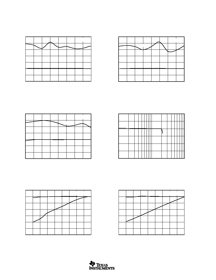
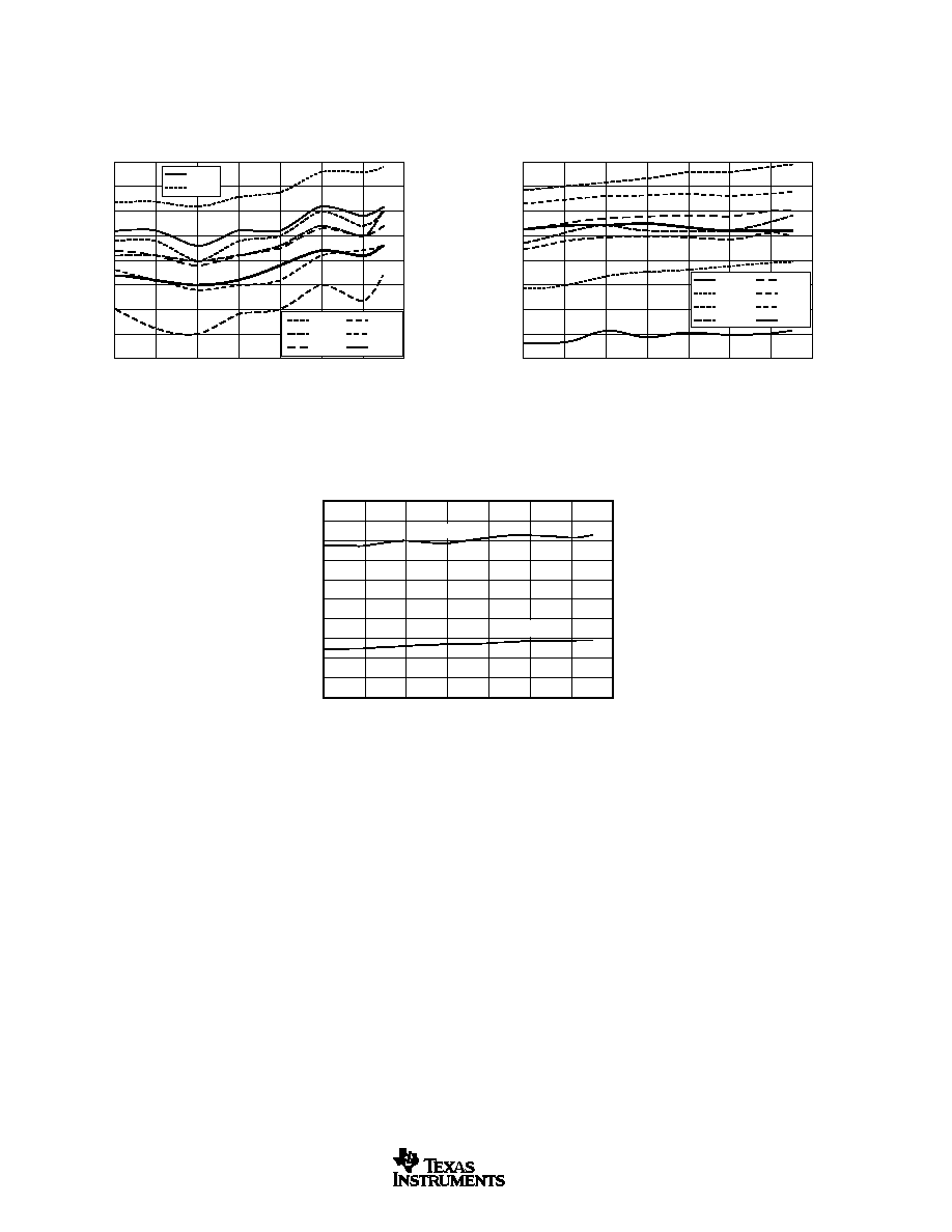
TYPICAL CHARACTERISTICS
(Cont.)
T
A
= 25
∞
C, AV
DD
= DV
DD
= 1.8V, DRV
DD
= 3.3V, f
IN
= ≠0.5dBFS, Internal Reference, Clock = 40MSPS, and Differential Input Range = 1Vp-p, unless otherwise noted.
SNR AND SFDR vs CLOCK FREQUENCY
SNR (dB), SFDR (dBc)
Clock Frequency (MSPS)
5
10
15
25
20
30
35
40
45
85
80
75
70
65
60
55
50
SNR
f
IN
= 3.5MHz
SFDR
SNR AND SFDR vs CLOCK FREQUENCY
SNR (dB), SFDR (dBc)
Clock Frequency (MSPS)
5
10
20
15
25
30
35
40
45
85
80
75
70
65
60
55
50
SNR
f
IN
= 10MHz
SFDR
SNR AND SFDR vs CLOCK FREQUENCY
SNR (dB), SFDR (dBc)
Clock Frequency (MHz)
5
25
20
15
10
30
35
40
45
80
75
70
65
60
55
50
45
SNR
f
IN
= 20MHz
SFDR
SNR vs INPUT FREQUENCY
SNR (dB)
Input Frequency (MHz)
1
10
100
68
64
60
56
52
48
44
SWEPT INPUT POWER (SNR)
SNR (dBFS, dBc)
Input Amplitude (dBFS)
≠45
≠40
≠35
≠25
≠30
≠20
≠15
≠10
≠5
0
70
60
50
40
30
20
10
0
dBc
f
IN
= 3.5MHz
dBFS
SWEPT INPUT POWER
SNR (dBFS, dBc)
Input Amplitude (dBFS)
≠45
≠40
≠35
≠25
≠30
≠20
≠15
≠10
≠5
0
70
60
50
40
30
20
10
0
dBc
f
IN
= 10MHz
dBFS
ADS5121
9
SBAS281
www.ti.com
TYPICAL CHARACTERISTICS
(Cont.)
T
A
= 25
∞
C, AV
DD
= DV
DD
= 1.8V, DRV
DD
= 3.3V, f
IN
= ≠0.5dBFS, Internal Reference, Clock = 40MSPS, and Differential Input Range = 1Vp-p, unless otherwise noted.
DYNAMIC PERFORMANCE vs DUTY CYCLE
SINAD (dB)
Clock Duty Cycle (%)
25
30
35
45
40
50
55
60
65
70
75
80
78
76
74
72
70
68
66
64
62
60
58
56
54
f
IN
= 3.5MHz
SNR
SFDR
SINAD
IAV
DD
vs CLOCK FREQUENCY
IAV
DD
(mA)
Clock Frequency (MSPS)
5
10
20
15
25
30
35
40
45
157.6
157.4
157.2
157.0
156.8
156.6
156.4
156.2
156.0
IDV
DD
vs CLOCK FREQUENCY
IDV
DD
(mA)
Clock Frequency (MSPS)
5
10
20
15
25
30
35
40
45
60
50
40
30
20
10
0
IDRV
DD
vs CLOCK FREQUENCY
IDRV
DD
(mA)
Clock Frequency (MSPS)
5
10
20
15
25
30
35
40
45
60
50
40
30
20
10
0
IDRV
DD
= 3.3V
IDRV
DD
= 1.8V
TOP REFERENCE vs TEMPERATURE
Top Reference (V)
Temperature (
∞
C)
≠40
≠20
20
0
40
60
80
100
1.348
1.347
1.347
1.346
1.346
1.345
1.345
1.344
1.344
BOTTOM REFERENCE vs TEMPERATURE
Bottom Reference (V)
Temperature (
∞
C)
≠40
≠20
20
0
40
60
80
100
0.824
0.824
0.823
0.823
0.822
0.822
0.821
0.821
0.820
0.820
ADS5121
10
SBAS281
www.ti.com
TYPICAL CHARACTERISTICS
(Cont.)
T
A
= 25
∞
C, AV
DD
= DV
DD
= 1.8V, DRV
DD
= 3.3V, f
IN
= ≠0.5dBFS, Internal Reference, Clock = 40MSPS, and Differential Input Range = 1Vp-p, unless otherwise noted.
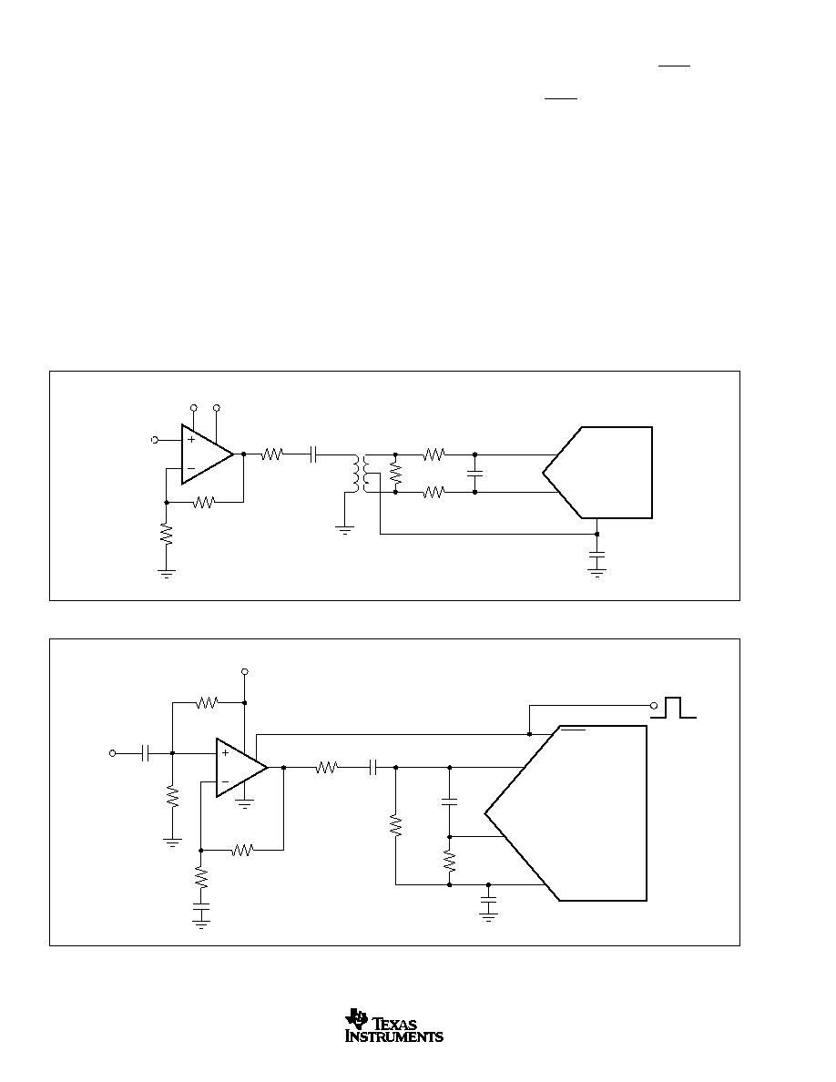
GAIN ERROR vs TEMPERATURE
Gain Error (%)
Temperature (
∞
C)
≠40
≠20
0
40
20
60
80
100
0
≠0.05
≠0.10
≠0.15
≠0.20
≠0.25
≠0.30
≠0.35
≠0.40
Ch-A
Ch-B
Ch-E
Ch-F
Ch-G
Ch-C
Ch-D
Ch-H
POWER vs TEMPERATURE
Power (mW)
Temperature (
∞
C)
≠40
≠20
20
0
40
60
80
100
550
530
510
490
470
450
430
410
390
370
350
1.8V DRV
DD
3.3V DRV
DD
ZERO ERROR vs TEMPERATURE
Error (%)
Temperature (
∞
C)
≠40
≠20
0
40
20
60
80
100
0
≠0.1
≠0.2
≠0.3
≠0.4
≠0.5
≠0.6
≠0.7
≠0.8
≠0.9
≠1.0
Ch-A
Ch-B
Ch-C
Ch-D
Ch-E
Ch-F
Ch-G
Ch-H

ADS5121
11
SBAS281
www.ti.com
APPLICATION INFORMATION
CONVERTER OPERATION
The ADS5121 is an 8-channel, simultaneous sampling ADC.
Its low power and high sampling rate of 40MSPS is achieved
using a state-of-the-art switched capacitor pipeline architec-
ture built on an advanced low-voltage CMOS process. The
ADS5121 operates primarily from a +1.8V single supply. For
additional interfacing flexibility, the digital I/O supply (DRV
DD
)
can be set to either +1.8V or +3.3V. The ADC core of each
channel consists of 10 pipeline stages. Each of the 10 stages
produces one digital bit per stage. Both the rising and the
falling clock edges are utilized to propagate the sample
through the pipeline every half clock, for a total of five clock
cycles. Two additional clock cycles are needed to pass the
sample data through the digital error correction logic and the
output latches. The total pipeline delay, or data latency, is
therefore 6.5 clock cycles long. Since a common clock
controls the timing of all eight channels, the analog signal is
sampled at the same time, as well as the data on the parallel
ports that become updated simultaneously.
INPUT IMPEDANCE
Due to the switched capacitor input, the input impedance of
the ADS5121 is effectively capacitive, and the driving source
needs to provide sufficient slew current to charge and dis-
charge the input sampling capacitor. The input impedance of
the ADS5121 is also a function of the sampling rate. As the
sampling frequency increases, the input impedance de-
creases at a linear rate of 1/fs. For most applications, this
does not represent a limitation since the impedance remains
relatively high, for example, approximately 31k
at the max
sampling rate of 40MSPS. For applications using an op amp
to drive the ADC, it is recommended that a series resistor,
typically 10
to 50
, be added between the amplifier's
output and the converter inputs. This will isolate the converter's
capacitive input from the driver and avoid potential gain
peaking, or instability.
INPUT BIASING
The ADS5121 operates from a single +1.8V analog supply,
and requires each of the analog inputs (AIN+, AIN≠) to be
externally biased by a suitable common-mode voltage. For
example, with a common-mode voltage of +1V, the 1V
PP
full-
scale, differential input signal will swing symmetrically around
+1V, or between 0.75V and 1.25V. This is determined by the
two reference voltages, the top reference (REFT), and the
bottom reference (REFB). Typically, the input common-mode
level is related to the reference voltages and defined as
(REFT + REFB)/2. This reference mid-point is provided at the
common-mode level output (CML) pin and can directly be
used for input biasing purposes. The voltage at CML will
assume the mid-point for either internal or external reference
operation. In any case, it is recommended to bypass the CML
pin with a ceramic 0.1
µ
F capacitor.
DRIVING THE ANALOG INPUTS
Differential versus Single-Ended
The analog input of the ADS5121 allows it to be driven either
single-ended or differentially. Differential operation of the
ADS5121 requires an input signal that consists of an in-
phase and a 180
∞
out-of-phase part simultaneously applied
to the inputs (AIN+, AIN≠). The differential operation offers a
number of advantages, which in most applications will be
instrumental in achieving the best dynamic performance of
the ADS5121:
∑ Signal swing is half that required for the single-ended
operation and is therefore less demanding to achieve while
maintaining good linearity performance from the signal
source.
∑ Reduced signal swing allows for more headroom of the
interface circuitry and therefore a wider selection of the
best suitable driver op amp.
∑ Even-order harmonics are minimized.
∑ Improved noise immunity based on the converter's com-
mon-mode input rejection.
For the single-ended mode, the signal is applied to one of the
inputs while the other input is biased with a DC voltage to the
required common-mode level. Both inputs are identical in
terms of their impedance and performance. Applying the
signal to the complementary input (AIN≠) instead of the AIN+
input, however, will invert the orientation of the input signal
relative to the output code. This could be helpful, for ex-
ample, if the input driver operates in inverting mode using
input AIN≠ as the signal input will restore the phase of the
signal to its original orientation.
INPUT DRIVER CONFIGURATIONS
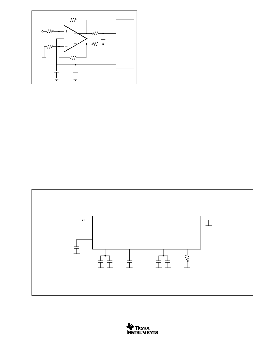
Transformer-Coupled Interface
If the application requires a signal conversion from a single-
ended source to drive the ADS5121 differentially, an RF-
transformer might be a good solution. The selected trans-
former must have a center tap in order to apply the common-
mode DC voltage necessary to bias the converter inputs. AC-
grounding the center tap will generate the differential signal
swing across the secondary winding. Consider a step-up
transformer to take advantage of signal amplification without
the introduction of another noise source. Furthermore, the
reduced signal swing from the source may lead to an im-
proved distortion performance.
ADS5121
12
SBAS281
www.ti.com
The differential input configuration may provide a noticeable
advantage of achieving good SFDR performance over a
wide range of input frequencies. In this mode, both inputs
(AIN+ and AIN≠) of the ADS5121 see matched impedances.
Figure 1 shows the schematic for the suggested transformer-
coupled interface circuit. The component values of the R-C
low-pass may be optimized depending on the desired roll-off
frequency.
Single-Ended, AC-Coupled Driver
The circuit of Figure 2 shows an example for driving the
inputs of the ADS5121 in a single-ended configuration. The
signal is AC-coupled between the driver amplifier and the
converter input (AIN+). This allows for setting the required
common-mode voltages for the ADC and op amp separately.
The single-supply op amp is biased at mid-supply by two
resistors connected at its noninverting input. Connecting
each input to the CML pin provides the required common-
mode voltage for the inputs of the ADS5121. Here, two
resistors of equal value ensure that the inputs see closely
matched source impedances. If the op amp features a
disable function, it could be easily tied together with the
power-down pin of the ADS5121 channel (STBY). In the
circuit example depicted in Figure 2, the OPA355's EN pin is
directly connected to the STBY pin to allow for a power-down
mode of the entire circuit. Other suitable op amps for single-
supply driver applications include the OPA634, OPA635, or
OPA690, for example.
DC-Coupled Interface with Differential Amplifier
Differential input/output amplifiers can simplify the driver
circuit for applications requiring input DC-coupling. Flexible in
their configurations, such amplifiers can be used for single-
ended to differential conversion, allow for signal amplifica-
tion, and also for filtering prior to the ADC. See Figure 3 for
one possible circuit implementation using the THS4130 am-
plifier. Here, the amplifier operates with a gain of +1. The
common- mode voltage available at the CML pin can be
conveniently connected to the amplifier's VOCM pin to set
the required input bias for the ADS5121.
FIGURE 1. Converting a Single-Ended Input Signal into a Differential Signal Using an RF-Transformer.
FIGURE 2. Single-Ended, AC-Coupled Driver Configuration for a Single Supply.
R
IN
R
IN
C
IN
0.1
µ
F
R
T
0.1
µ
F
1:n
R
S
OPA690
R
1
R
2
V
IN
ADS5121
AIN+
AIN≠
CML
≠5V
+5V
OPA355
V
IN
R
F
604
R
G
604
1.82k
1.82k
ADS5121
R
S
24
EN
33pF
0.1
µ
F
0.1
µ
F
R
1
AIN+
STBY
CML
AIN≠
0.1
µ
F
0.1
µ
F
R
2
+3V/+5V
ADS5121
13
SBAS281
www.ti.com
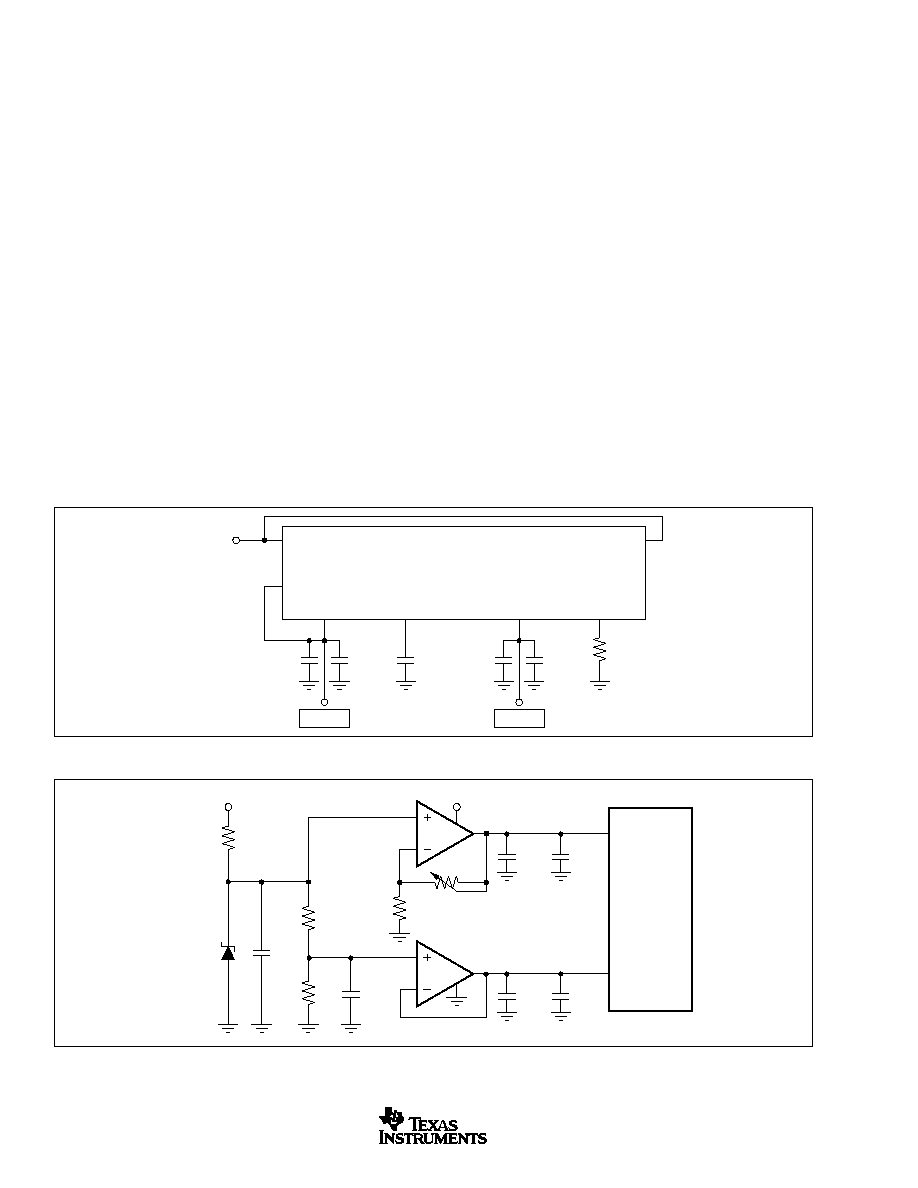
REFERENCE OPERATION
For proper operation of the ADS5121 and its reference,
an external 6.8k
resistor must be connected from the
IREFR pin to analog ground (AGND), as shown in Figure 4.
While a 1% resistor tolerance is adequate, deviating from this
resistor value will cause altered and degraded performance.
To ensure proper operation with any reference configuration, it
is necessary to provide solid bypassing at all reference pins in
order to keep the clock feedthrough to a minimum. Figure 4
shows the recommended decoupling scheme. Good perfor-
mance can be obtained using 0.1
µ
F low inductance ceramic
capacitors. Adding tantalum capacitors (1
µ
F to 10
µ
F) may lead
to a performance improvement, depending on the application.
All bypassing capacitors should be located as close as pos-
sible to their respective pins.
INTERNAL REFERENCE
The internal reference circuit of the ADS5121 consists of a
bandgap voltage reference, the drivers for the top and
bottom reference, and the resistive reference ladder. The
corresponding reference pins are REFT, REFB, CML, IREFR,
BG, and PDREF. In order to enable the internal reference,
PDREF must be at a logic LOW (= 0) level. In addition, the
bandgap pin BG should be decoupled with a 0.1
µ
F capacitor.
The reference circuit provides the reference voltages to each
of the eight channels.
The reference buffers can be utilized to supply up to 1mA
(sink and source) to an external circuitry. The CML pin
represents the mid-point of the internal resistor ladder and is
an unbuffered node. Loading of this pin should be avoided,
as it will lead to degradation of the converter's linearity.
USING EXTERNAL REFERENCES
For even more design flexibility, the internal reference can be
disabled and an external reference voltage used. The utiliza-
tion of an external reference may be considered for applica-
tions requiring higher accuracy or improved temperature
performance. Especially in multi-channel applications, the
use of a common external reference has the benefit of
obtaining better matching of the full-scale range between
converters.
Setting the ADS5121 for external reference mode requires
taking the PDREF pin HIGH. In addition, pins BG and REFT
must be connected together (see Figure 5). The common-
mode voltage at the CML pin will be maintained at approxi-
mately the mid-point of the applied reference voltages, ac-
cording to CML
(VREFT ≠ VREFB)/2. The internal buffer
FIGURE 3. DC-Coupled Interface Using Differential I/O Amplifier
THS4130.
V
IN+
V
OCM
0.1
µ
F
2.2
µ
F
47pF
390
390
390
390
20
20
CML
AIN≠
AIN+
ADS5121
THS4130
FIGURE 4. Internal Reference; Recommended Configuration and Bypassing.
6.8k
2.2
µ
F
+
0.1
µ
F
0.1
µ
F
0.1
µ
F
BG
REFT
CML
ADS5121
REFB
IREFR
AV
DD
PDREF
2.2
µ
F
+
0.1
µ
F
+1.8V
ADS5121
14
SBAS281
www.ti.com
amplifiers for REFT and REFB are disabled when the
ADS5121 operates in the external reference mode. The
external reference circuit must be designed to drive the
internal reference ladder (80
) located between the REFT
and REFB pins. For example, setting REFT = +1.25V and
REFB = +0.75V will require a current drive capability of at
least 0.5V/ 80
= 6.25mA. The external references can vary
as long as the value of the external top reference (REFT
EXT
)
stays within the range of +1.15V to +1.35V, and the external
bottom reference (REFB
EXT
) stays within +0.65V to +0.85V
(as shown in Figure 6).
DIGITAL INPUTS AND OUTPUTS
Clock Input
The clock input is designed to operate with +1.8V or +3.3V
CMOS logic levels. The clock circuitry is internally connected
to the DRV
DD
supply. Therefore, the input HIGH and LOW
levels will vary depending on the applied DRV
DD
supply, see
the DC Characteristic tables. Since both edges of the clock
are used in this pipeline ADC, the ideal clock should be a
square-wave logic signal with a 50% duty-cycle.
Since this condition cannot always easily be met, the ADS5121
features an internal clock conditioning circuitry that can be
activated through the duty-cycle adjust pin (DCASEL).
The DCASEL pin is a logic input, with its logic levels related
to the DV
DD
supply (+1.8V only):
a) DCASEL = LOW (GND); in this mode the clock condition-
ing circuitry is disabled. Use this setting if the applied
clock signal is a square-wave clock with a duty cycle of
50%, or if the duty cycle stays within a range of 48% to
52%.
b) DCASEL = HIGH (DV
DD
); in this mode the clock condition-
ing circuitry is enabled. Use this setting if the applied
external clock signal is a square-wave clock that does not
meet the criteria listed above, but has a duty cycle in the
range of 30% to 70%.
MINIMUM SAMPLING RATE
The pipeline architecture of the ADS5121 uses a switched
capacitor technique for the internal track-and-hold stages.
With each clock cycle, charges representing the captured
signal level are moved within the ADC pipeline core. The
high sampling rate necessitates the use of very small capaci-
tor values. In order to hold the droop errors low, the capaci-
tors require a minimum `refresh rate'. To maintain full accu-
racy of the acquired sample charge, the sampling clock of the
ADS5121 should not be lower than the specified minimum of
5MSPS.
FIGURE 5. External Reference; Recommended Configuration and Bypassing.
6.8k
2.2
µ
F
0.1
µ
F
+
0.1
µ
F
BG
REFT
REFT
EXT
CML
ADS5121
REFB
IREFR
AV
DD
+1.8V
PDREF
2.2
µ
F
+
0.1
µ
F
REFB
EXT
FIGURE 6. Circuit Example of an External Reference Circuit Using a Single-Supply, Low-Power, Dual Op Amp (OPA2234).
R
3
R
4
R
1
R
2
+
+
2.2
µ
F
0.1
µ
F
0.1
µ
F
+
2.2
µ
F
0.1
µ
F
10
µ
F
REFT
REFB
ADS5121
1/2
OPA2234
1/2
OPA2234
4.7k
+5V
+5V
REF1004
+2.5V
ADS5121
15
SBAS281
www.ti.com
DATA OUTPUT FORMAT
The output data format of the ADS5121 is a positive Straight
Offset Binary (SOB) code. Tables I and II show output coding
of a single-ended and differential signal. For all data output
channels, the MSBs are located at the D9x pins.
channels. Note that the OE pin has no internal pull-up
resistor and therefore requires a defined potential to be
applied. The timing relations between OE and the output bus
enable/disable times are shown in the Timing Diagram.
POWER-DOWN (STANDBY)
The ADS5121 is equipped with a power-down function for
each of the eight channels. Labeled as STBY pins, the
channel is in normal operating mode when the STBY pin is
connected to logic high (H = 1). The selected ADC channel
will be in a power-down mode if the corresponding STBY pin
is connected to logic LOW (L = 0). The logic levels for the
STBY pins are dependent on the DRV
DD
supply. The power-
down function controls internal biasing nodes, and as a
consequence, any data present in the pipeline of the con-
verter will become invalid. This is independent of whether the
clock remains applied during power-down or not. Following a
power-up, new valid data will become available after a
minimum of seven clock cycles. As a note, the operation of
the STBY pins is not intended for the use of dynamically
multiplexing between the eight channels of the ADS5121.
DIGITAL OUTPUT DRIVER SUPPLY, DRV
DD
The ADS5121 uses a dedicated supply connection for the
output logic drivers, DRV
DD
, along with its digital driver
ground connections, labeled DRGND.
Setting the voltage at DRV
DD
to either +3.3V or +1.8V also
sets the output logic levels accordingly, allowing the ADS5121
to directly interface to a selected logic family. The output
stages are designed to supply sufficient current to drive a
variety of logic families. However, it is recommended to use
the ADS5121 with a +1.8V driver supply. This will lower the
power dissipation in the output stages due to the lower output
swing and reduce current glitches on the supply lines, which
otherwise may affect the AC performance of the converter. In
some applications it might be advantageous to decouple the
DRV
DD
supply with additional capacitors or a pi-filter.
GROUNDING AND DECOUPLING
Proper grounding and bypassing, short lead length, and the
use of ground planes are particularly important for high-
frequency designs. Multilayer pc-boards are recommended
for best performance since they offer distinct advantages
such as minimizing ground impedance, separation of signal
layers by ground layers, etc. The ADS5121 should be treated
as an analog component. Whenever possible, the supply
pins should be powered by the analog supply. This will
ensure the most consistent results, since digital supply lines
often carry high levels of noise which otherwise would be
coupled into the converter and degrade the achievable per-
formance. The ground pins should directly connect to an
analog ground plane covering the pc-board area under the
converter. While designing the layout it is important to keep
the analog signal traces separated from any digital line to
prevent noise coupling onto the analog signal path. Due to its
high sampling rate, the ADS5121 generates high-frequency
current transients and noise (clock feedthrough) that are fed
SINGLE-ENDED INPUT
STRAIGHT OFFSET BINARY
(AIN≠ = CML)
(SOB)
+FS ≠ 1LSB (AIN+ = CML + FSR/2)
11 1111 1111
+1/2 FS
11 0000 0000
Bipolar Zero (AIN+ = CML)
10 0000 0000
≠1/2 FS
01 0000 0000
≠FS (AIN+ = CML ≠ FSR/2)
00 0000 0000
TABLE I. Coding Table for Single-Ended Input Configuration
with Input AIN≠ Tied to the Common-Mode Volt-
age (CML).
STRAIGHT OFFSET BINARY
DIFFERENTIAL INPUT
(SOB)
+FS ≠ 1LSB (AIN+ = REFT, AIN≠ = REFB)
11 1111 1111
+1/2 FS
11 0000 0000
Bipolar Zero (AIN+ = AIN≠ = CML)
10 0000 0000
≠1/2 FS
01 0000 0000
≠FS (AIN+ = REFB, AIN≠ = REFT)
00 0000 0000
TABLE II. Coding Table for Differential Input Configuration
and 1V
PP
Full-Scale Range.
DIGITAL OUTPUT LOADING
Minimizing the capacitive loading on the digital outputs is
very important in achieving the best performance. The total
load capacitance is typically made up of two sources: the
next stage input capacitance, and the parasitic/pc-board
capacitance. It is recommended to keep the total capacitive
loading on the data lines as low as possible (
20pF). Higher
capacitive loading will cause larger dynamic currents as the
digital outputs are dynamic states. High current surges may
cause feedback into the analog portion of the ADS5121 and
affect the performance. If necessary, external buffers or
latches close to the converter's output pins may be used to
minimize the capacitive loading. A suggested device is the
SN74AVC16827 (20-bit buffer/driver), a member of the `Ad-
vanced Very Low Voltage CMOS' logic family (AVC). Using
such a logic device can also provide the added benefit of
isolating the ADS5121 from any digital noise activities on the
bus coupling back high-frequency noise. Some applications
may also benefit from the use of series resistors (
100
) in
the data lines. This will provide a current limit and reduce any
existing over- or undershoot.
OUTPUT ENABLE
The ADS5121 provides one output enable pin (OE) that
controls the digital outputs of all channels simultaneously. A
LOW (L = 0) level on the OE pin will have all channels active
and the converter in normal operation. Taking the OE pin
HIGH (H = 1) will disable or tri-state the outputs of all

ADS5121
16
SBAS281
www.ti.com
back into the supply and reference lines. This requires that all
supply and reference pins are sufficiently bypassed. In most
cases 0.1
µ
F ceramic chip capacitors at each pin are ad-
equate to keep the impedance low over a wide frequency
range. Their effectiveness depends largely on the proximity
to the individual supply pin. Therefore, they should be lo-
cated as close as possible to the supply pins. In addition, a
larger bipolar capacitor (1
µ
F to 22
µ
F) should be placed on
the pc-board in proximity to the converter circuit.
LAYOUT OF THE PCB WITH A
MICROSTAR BGA PACKAGE
The ADS5121 is housed in a polymide film-based chipscale
package (CSP). Like most CSPs, solder alloy balls are used
as the interconnect between the package substrate and the
board on which the package is soldered. For detailed infor-
mation regarding these packages, please refer to literature
number SSYZ015B, MicroStar BGA Packaging Reference
Guide, which addresses the specific considerations required
when integrating a MicroStar BGA package into the PCB
design. This document can be found at:
http://www-s.ti.com/sc/psheets/ssyz015b/ssyz015b.pdf
TERMINOLOGY
ANALOG BANDWIDTH
The analog input frequency at which the spectral power of
the fundamental frequency (as determined by the FFT analy-
sis) is reduced by 3dB.
APERTURE DELAY
The delay between the 50% point of the rising edge of the
clock and the instant at which the analog input is sampled.
APERTURE UNCERTAINTY (JITTER)
The sample-to-sample variation in aperture delay.
EFFECTIVE NUMBER OF BITS (ENOB)
The ENOB is calculated from the measured SINAD based on
the equation:
ENOB
SINAD
dB
=
≠ .
.
1 76
6 02
EFFECTIVE RESOLUTION BANDWIDTH
The maximum analog input frequency at which the SINAD is
decreased by 3dB or the ENOB by half a bit.
GAIN ERROR
Gain Error is the deviation of the actual difference between
first and last code transitions and the ideal difference be-
tween first and last code transitions.
GAIN MATCHING
Variation in Gain Error between adjacent channels.
2ND-HARMONIC DISTORTION
The ratio of the rms signal amplitude to the rms value of the
2nd-harmonic component, reported in dBc.
3RD-HARMONIC DISTORTION
The ratio of the rms signal amplitude to the rms value of the
3rd-harmonic component, reported in dBc.
INTERMODULATION DISTORTION (IMD)
The 2-tone IMD is the ratio expressed in decibels of either
input tone to the worst 3rd-order (or higher) Intermodulation
products. The individual input tone levels are at ≠6.5dB full-
scale, and their envelope is at ≠0.5dB full-scale.
OFFSET ERROR (ZERO-SCALE ERROR)
The first transition should occur for an analog value 1/2 LSB
above negative full-scale. Offset error is defined as the
deviation of the actual transition from that point.
OFFSET MATCHING
The change in offset error between adjacent channels.
POWER-SUPPLY REJECTION RATIO (PSRR)
The ratio of a change in input offset voltage to a change in
power-supply voltage.
SIGNAL-TO-NOISE AND DISTORTION (SINAD)
The ratio of the rms signal amplitude (set 0.5dB below full-
scale) to the rms value of the sum all other spectral compo-
nents, including harmonics but excluding DC.
SIGNAL-TO-NOISE RATIO (WITHOUT HARMONICS)
The ratio of the rms signal amplitude (set 0.5dB below full-
scale) to the rms value of the sum of all other spectral
components, excluding the first five harmonics and DC.
SPURIOUS-FREE DYNAMIC RANGE (SFDR)
The ratio of the rms signal amplitude to the rms value of the
peak spurious spectral component. The peak spurious com-
ponent may or may not be a harmonic. May be reported in
dBc (i.e., degrades as signal level is lowered), or dBFS
(always related back to converter full-scale).
ADS5121
17
SBAS281
www.ti.com
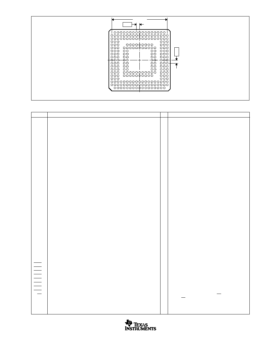
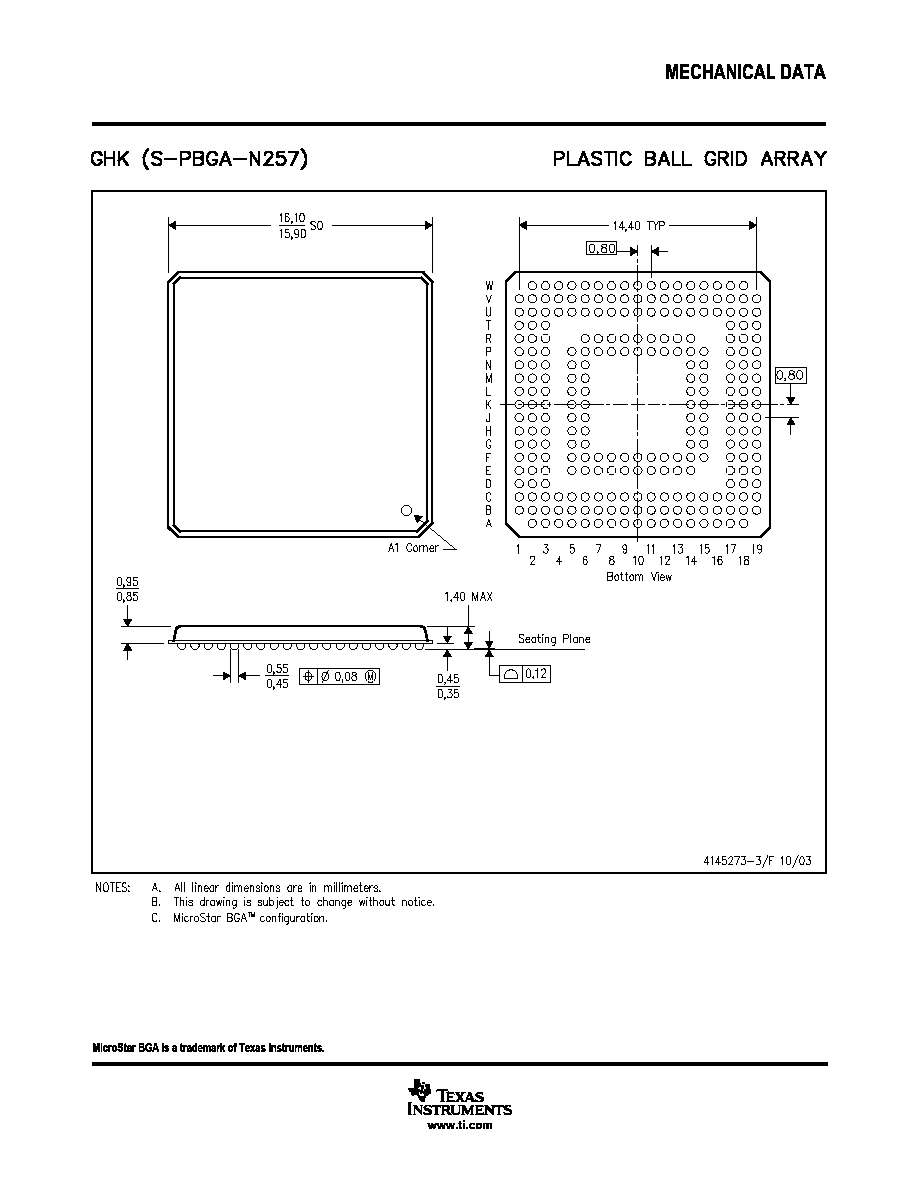
PACKAGE DRAWING
GHK (S-PBGA-N257)
PLASTIC BALL GRID ARRAY
19
14,40 TYP
17
16
13
14
15
11
12
9
8
10
V
U
W
R
N
P
L
M
K
T
7
5
6
3
4
H
F
G
E
C
D
1
A
B
2
J
18
Seating Plane
4145273-3/C 12/99
SQ
16,10
15,90
0,95
0,45
0,35
0,55
0,45
0,12
0,08
0,85
1,40 MAX
0,10
0,80
M
0,08
0,80
NOTES: A. All linear dimensions are in millimeters.
B. This drawing is subject to change without notice.
C. MicroStar BGA configuration
TM

PACKAGING INFORMATION
ORDERABLE DEVICE
STATUS(1)
PACKAGE TYPE
PACKAGE DRAWING
PINS
PACKAGE QTY
ADS5121IGHK
ACTIVE
BGA
GHK
257
90
(1) The marketing status values are defined as follows:
ACTIVE: Product device recommended for new designs.
LIFEBUY: TI has announced that the device will be discontinued, and a lifetime-buy period is in effect.
NRND: Not recommended for new designs. Device is in production to support existing customers, but TI does not recommend using this part in
a new design.
PREVIEW: Device has been announced but is not in production. Samples may or may not be available.
OBSOLETE: TI has discontinued the production of the device.
PACKAGE OPTION ADDENDUM
www.ti.com
3-Oct-2003

IMPORTANT NOTICE
Texas Instruments Incorporated and its subsidiaries (TI) reserve the right to make corrections, modifications,
enhancements, improvements, and other changes to its products and services at any time and to discontinue
any product or service without notice. Customers should obtain the latest relevant information before placing
orders and should verify that such information is current and complete. All products are sold subject to TI's terms
and conditions of sale supplied at the time of order acknowledgment.
TI warrants performance of its hardware products to the specifications applicable at the time of sale in
accordance with TI's standard warranty. Testing and other quality control techniques are used to the extent TI
deems necessary to support this warranty. Except where mandated by government requirements, testing of all
parameters of each product is not necessarily performed.
TI assumes no liability for applications assistance or customer product design. Customers are responsible for
their products and applications using TI components. To minimize the risks associated with customer products
and applications, customers should provide adequate design and operating safeguards.
TI does not warrant or represent that any license, either express or implied, is granted under any TI patent right,
copyright, mask work right, or other TI intellectual property right relating to any combination, machine, or process
in which TI products or services are used. Information published by TI regarding third-party products or services
does not constitute a license from TI to use such products or services or a warranty or endorsement thereof.
Use of such information may require a license from a third party under the patents or other intellectual property
of the third party, or a license from TI under the patents or other intellectual property of TI.
Reproduction of information in TI data books or data sheets is permissible only if reproduction is without
alteration and is accompanied by all associated warranties, conditions, limitations, and notices. Reproduction
of this information with alteration is an unfair and deceptive business practice. TI is not responsible or liable for
such altered documentation.
Resale of TI products or services with statements different from or beyond the parameters stated by TI for that
product or service voids all express and any implied warranties for the associated TI product or service and
is an unfair and deceptive business practice. TI is not responsible or liable for any such statements.
Following are URLs where you can obtain information on other Texas Instruments products and application
solutions:
Products
Applications
Amplifiers
amplifier.ti.com
Audio
www.ti.com/audio
Data Converters
dataconverter.ti.com
Automotive
www.ti.com/automotive
DSP
dsp.ti.com
Broadband
www.ti.com/broadband
Interface
interface.ti.com
Digital Control
www.ti.com/digitalcontrol
Logic
logic.ti.com
Military
www.ti.com/military
Power Mgmt
power.ti.com
Optical Networking
www.ti.com/opticalnetwork
Microcontrollers
microcontroller.ti.com
Security
www.ti.com/security
Telephony
www.ti.com/telephony
Video & Imaging
www.ti.com/video
Wireless
www.ti.com/wireless
Mailing Address:
Texas Instruments
Post Office Box 655303 Dallas, Texas 75265
Copyright
2003, Texas Instruments Incorporated