ADSL Analog Front End
Copyright © 2000, Texas Instruments Incorporated
SBWS014
Printed in U.S.A. December, 2000
ADSL ANALOG FRONT-END
FEATURES
q
NOISE FLOOR: 144dBm/Hz
q
MULTIRATE COMPATIBLE
q
VCXO CIRCUITRY AND DAC
AFE1302
DESCRIPTION
Burr-Brown's Analog Front-End from Texas Instru-
ments reduces the size and cost of an ADSL-compliant
system by providing the active analog circuitry needed
to connect an ADSL Digital Signal Processor (DSP) to
an external line driver, receiver, TX/RX filters, hy-
brid, transformer, and POTS filter. The AFE1302 is
designed for downstream data rates of 4Mbps and
higher, and operation at a clock rate of 35.328MHz,
with an output word rate of up to 8.832MWords/s.
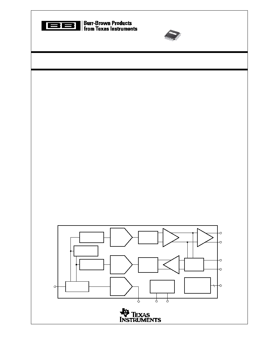
Functionally, this unit consists of a transmit (TX) chan-
nel, a receive (RX) channel, a VCXO (Voltage Con-
trolled Crystal Oscillator) control Digital-to-Analog
Converter (DAC), and VCXO active circuitry. The TX
section converts, filters, and buffers outgoing Discrete
Multi Tone (DMT) data from the ADSL DSP.
The receive section amplifies, filters, and digitizes the
DMT data received on the twisted pair line.
This IC operates on a single 5V supply. The digital
circuitry in the unit can be connected to a supply voltage
ranging from 3.3V to 5V. The chip uses only 570mW.
The AFE1302 is designed to be used with external
amplifiers and filters for noise reduction and dynamic-
range improvement.
The RX channel consists of a low-noise PGA, a switched
capacitor low-pass filter, and fourth-order delta-sigma
Analog-to-Digital Converter (ADC). The delta-sigma
modulator operating at a 32X oversampling ratio pro-
duces a 16-bit output at word rates up to 8832kHz.
The TX channel consists of a fourth-order delta-sigma
DAC, switched-capacitor low-pass filter, program-
mable attenuator, and buffer. The buffer drives off-
chip into a low-noise line driver configured as a 3-pole
active filter to produce an overall low-noise high-drive
TX output signal on a twisted pair line.
q
8.8M TO 1.1MWords/s WORD RATE
q
FIVE GENERAL-PURPOSE OUTPUTS
q
570mW POWER DISSIPATION
q
TQFP-48 PACKAGE
16-Bit
DAC
16-Bit
ADC
VCXO
DAC
Atten
PGA
Interpolation
Filter
Decimation
Filter
Analog
Loop Back
General Purpose
Digital Output
VCXO
Active Ckts
Buffer
LP
Filter
LP
Filter
Digital
Interface
From DSP
TX Output
RX Input
5
AFE1302
Digital
Loopback
Patents Pending
www.ti.com
AFE1
302
AFE1302
2
SBWS014
SPECIFICATIONS
Typical at 25
°
C, AV
DD
= +5V, DV
DD
= +3.3V, f
CLK
= 35.328MHz, TX output and RX input measured differentially, unless otherwise specified.
AFE1302Y
PARAMETER
CONDITIONS
MIN
TYP
MAX
UNITS
RECEIVE CHANNEL
Input Signal (CMV = AV
DD
/2)
Differential, G = 6dB
9.0
9.6
Vp-p
Common-Mode Voltage
AV
DD
/2
V
Input Impedance
Pin-to-AV
DD
2.8
k
Input Capacitance
30
pF
Programmable Amplifier Range
6
40
dB
Gain Step Size
Monotonicity Guaranteed
1
dB
Input Noise
PGA = +40dB
(1)
148
144
dBm/Hz
Output Word Rate
1.104
8.832
MWords/s
Output Word Resolution
(15 Bits + 1 Sign Bit) or (14 Bits + 2 Sign Bits)
16
Bits
ADC Sampling Rate
35.328
MSamples/s
Low-Pass Frequency Corner
One Pole Analog Filter
1.1
MHz
Passband Droop
At 550kHz
1
dB
SINAD
PGA Gain = 40dB, Input Referred
100
dB
PGA Gain = 0dB
68
dB
THD
Single Tone, PGA = 0dB
75
84
dB
MTPR (MultiTone Power Ratio)
75
dB
TRANSMIT CHANNEL
Input Word Rate
1.104
8.832
MWords/s
Input Word Resolution
(15 Bits + 1 Sign Bit) or (14 Bits + 2 Sign Bits)
16
Bits
Peak Signal Amplitude
Differential, G = 0dB
4.4
4.8
Vp-p
Common-Mode Voltage
AV
DD
/2
Load Resistance
Differential
400
Load Capacitance
Differential
10
pF
Programmable Attenuator Range
31
0
dB
Attenuator Step Size
Monotonicity Guaranteed
1.0
dB
Attenuator Step Accuracy
0.5
dB
Low-Pass Filter Corner Frequency
Fourth-Order, 0.1dB Programmable
127
kHz
Passband Ripple
0.1
dB
Group Delay Variation
10
µ
s
Output Noise
Measured at 50kHz
110
dBm/Hz
Measured at 200kHz
116
dBm/Hz
THD Distortion
FS Output 0dB
65
dBc
FS Output 6dB
73
dBc
SFDR in RX Band (20 Tone Test)
See Note (2)
98
dBVrms
MTPR
70
dB
VCXO WITH EXTERNAL CIRCUITRY
Sensitive to PCB Layout
Frequency
35.328
MHz
Tuning Range
±
100
ppm
DAC Resolution
Monotonicity Guaranteed
10
Bits
DIGITAL INTERFACE
Logic Levels
V
IH
|I
IH
| < 10
µ
A
DV
DD
1
DV
DD
DV
DD
+ 0.3
V
V
IL
|I
IL
| < 10
µ
A
0.3
0
0.8
V
V
OH
I
OH
= 20
µ
A
DV
DD
0.5
V
V
OL
I
OL
= 20
µ
A
0.4
V
CONTROL INTERFACE (GC0, GC1, GP0, GP1, GP2)
Logic Levels
V
OH
I
OH
= 1mA
DV
DD
0.5
V
V
OL
I
OL
= 1mA
0.4
V
POWER
Analog Power Supply Voltage
AV
DD
4.75
5
5.25
V
Analog Dissipated Power
470
mW
Digital Power Supply Voltage
DV
DD
3.0
3.3
5.5
V
Digital Dissipated Power
V
DD
= 3.3V
100
mW
TEMPERATURE RANGE
Operation
0
70
°
C
Thermal Resistance,
JA
56.5
°
C/W
NOTES: (1) With TX in operation, no RX data, referred to 100
. (2) With TX reverb multitone signal (25.875kHz to 138kHz at a 4.3125kHz step), measured signal
level beyond 150kHz at TXP, TXN.
AFE1302
3
SBWS014
PIN CONFIGURATION
Top View
TQFP
ABSOLUTE MAXIMUM RATINGS
ELECTROSTATIC
DISCHARGE SENSITIVITY
This integrated circuit can be damaged by ESD. Burr-Brown
recommends that all integrated circuits be handled with
appropriate precautions. Failure to observe proper handling
and installation procedures can cause damage.
ESD damage can range from subtle performance degradation
to complete device failure. Precision integrated circuits may
be more susceptible to damage because very small parametric
changes could cause the device not to meet its published
specifications.
36
35
34
33
32
31
30
29
28
27
26
25
AV
SS
4
TXP
AV
DD
4
TXN
AV
SS
6
CMI
CMO
VREF1
VRNTX
VRPTX
VRNRX
VRPRX
CLKM
CLKNIB
DV
SS
2
AV
SS
1
XTALO
XTALI
AV
DD
1
VCXO
VREF2
AV
DD
2
AV
SS
2
AV
SS
5
CLIP
PDOWN
RESETN
GP2
GP1
GP0
RXN
RXP
AV
DD
3
AV
SS
3
GC1
GC0
1
2
3
4
5
6
7
8
9
10
11
12
CLWD
CTRLIN
DV
DD
1
DV
SS
1
TX3
TX2
TX1
TX0
RX3
RX2
RX1
RX0
48
47
46
45
44
43
42
41
40
39
38
13
14
15
16
17
18
19
20
21
22
23
37
24
AFE1302
PACKAGE
SPECIFIED
DRAWING
TEMPERATURE
PACKAGE
ORDERING
TRANSPORT
PRODUCT
PACKAGE
NUMBER
RANGE
MARKING
NUMBER
(1)
MEDIA
AFE1302Y
TQFP-48
355
0
°
C to +70
°
C
AFE1302Y
AFE1302Y/250
Tape and Reel
"
"
"
"
"
AFE1302Y/2K
Tape and Reel
NOTE: (1) Models with a slash (/) are available only in Tape and Reel in the quantities indicated (e.g., /2K indicates 2000 devices per reel). Ordering 2000 pieces
of "AFE1302Y/2K" will get a single 2000-piece Tape and Reel.
PACKAGE/ORDERING INFORMATION
Analog Inputs: Current .............................................
±
100mA, Momentary
±
10mA, Continuous
Voltage ................................. AGND 0.3V to AV
DD
+0.3V
Analog Outputs Short Circuit to Ground (+25
°
C) ................... Continuous
AV
DD
to AGND ....................................................................... 0.3V to 6V
DV
DD
to DGND ....................................................................... 0.3V to 6V
Digital Input Voltage to DGND ................................ 0.3V to DV
DD
+0.3V
Digital Output Voltage to DGND ............................. 0.3V to DV
DD
+0.3V
AGND, DGND, Differential Voltage .................................................... 0.3V
Junction Temperature (T
J
) ............................................................ +150
°
C
Storage Temperature Range ......................................... 40
°
C to +125
°
C
Lead Temperature (soldering, 3s) ................................................. +260
°
C
Power Dissipation .......................................................................... 700mW
AFE1302
4
SBWS014
PIN DESCRIPTIONS
Number
Type
Pin Name
Description
External Connection
Analog Interface
23
Output
GC0
External Gain Control Output LSB
Optional Swap Amp
24
Output
GC1
External Gain Control Output MSB
Optional Swap Amp
19
Input
RXN
Analog Receive Negative Input
Line Interface
20
Input
RXP
Analog Receive Positive Input
Line Interface
25
Output
VRPRX
RX Reference Positive Output
0.1uF,1
µ
F to AV
SS
3
26
Output
VRNRX
RX Reference Negative Output
0.1uF,1
µ
F to AV
SS
3
30
Output
CMO
Output Common-Mode voltage
0.1uF,1
µ
F to AV
SS
3
27
Output
VRPTX
TX Reference Positive Output
0.1uF,1
µ
F to AV
SS
3
28
Output
VRNTX
TX Reference Negative Output
0.1uF,1
µ
F to AV
SS
3
29
Output
VREF1
Unbuffered Bandgap Reference
0.1uF,1
µ
F to AV
SS
3
31
Output
CMI
Unbuffered Common-Mode Voltage
0.1uF,1
µ
F to AV
SS
3
35
Output
TXP
TX Positive Output
Line Interface
33
Output
TXN
TX Negative Output
Line Interface
40
Output
VREF2
DAC Reference Voltage
XTAL Interface
41
Output
VCXO
VXCO Control Voltage DAC Output
XTAL Interface
43
--
XTALI
XTAL Oscillator Input
XTAL
44
--
XTALO
XTAL Oscillator Output
XTAL
Digital Interface
48
Output
CLKM
Master Clock Output, f = 35.328MHz
DSP
47
Output
CLKNIB
Nibble Clock Output
DSP
1
Output
CLWD
Word Clock Output
DSP
2
Input
CTRLIN
Serial Data Input
DSP
5
Input
TX3
Digital Transmit Input
DSP
6
Input
TX2
Digital Transmit Input
DSP
7
Input
TX1
Digital Transmit Input
DSP
8
Input
TX0
Digital Transmit Input
DSP
9
Output
RX3
Digital Receive Output
DSP
10
Output
RX2
Digital Receive Output
DSP
11
Output
RX1
Digital Receive Output
DSP
12
Output
RX0
Digital Receive Output
DSP
13
Output
CLIP
Clipping Detection Output
DSP
14
Input
PDOWN
Power-Down Select, "1" = Power Down
DSP
15
Input
RESETN
Reset Pin (Active LOW)
DSP
16
Output
GP2
General-Purpose Output 2
--
17
Output
GP1
General-Purpose Output 1
--
18
Output
GP0
General-Purpose Output 0
--
Supply voltages
46
--
DV
SS
2
Digital Ground 2
DGND Plane
3
3V or 5V
DV
DD
1
Digital Power
0.1uF,1
µ
F to DV
SS
1
4
--
DV
SS
1
Digital Ground 1
DGND Plane
21
5V
AV
DD
3
Analog Power (Main)
0.1uF,1
µ
F to AV
SS
3
22
--
AV
SS
3
Analog Ground (Main)
AGND Plane
32
--
AV
SS
6
Analog Ground for TX Output
AGND Plane
34
5V
AV
DD
4
Analog Power for TX Output
0.1uF,1
µ
F to AV
SS
4
36
--
AV
SS
4
Analog Ground for TX Output
AGND Plane
37
--
AV
SS
5
Analog Clock Ground
AGND Plane
38
--
AV
SS
2
Analog Clock Ground
AGND Plane
39
5V
AV
DD
2
Analog Clock Power
0.1uF,1
µ
F to AV
SS
2
42
5V
AV
DD
1
XTAL Power
0.1uF,1
µ
F to AV
SS
1
45
--
AV
SS
1
XTAL Ground
AGND Plane
AFE1302
5
SBWS014
THEORY OF OPERATION
The AFE1302 consists of a transmit (TX) channel, a receive
(RX) channel, and a digital interface to connect to an ADSL
DSP. In addition, VCXO circuitry and a VCXO control
DAC are included for precise clock generation.
The TX channel receives digital data at the nominal rate of
1.104MWords/s to 8.832MWords/s. These TX data words
are interpolated up to the AFE1302 clock rate of 35.328MHz.
The data is converted to analog form with a 16-bit delta-
sigma DAC and bandwidth limited with a fourth-order,
switched-capacitor low-pass filter. The filter output is buff-
ered and drives off-chip to an external Burr-Brown line-
driver circuit from Texas Instruments. This line driver is
configured as an LC passive filter to provide additional out-
of-band noise and distortion attenuation (see System sec-
tion). Transmit power can be reduced with a combination of
digital and analog attenuation to ensure compliance with the
G.992.2 "politeness" rule.
In the RX channel, the analog receive signal is input to a PGA.
The output of the first-order, switched capacitor filter is digi-
tized with a 16-bit delta-sigma ADC. A decimation filter
ensures a compliant word rate (1.104MWords/s to
8.832MWords/s) to the ADSL digital chip.
Precise phase alignment is required to ensure proper opera-
tion of the ADSL modem. The active circuitry required to
create a VCXO is included on the AFE1302. This includes
the gain element as well as a 10-bit, monotonic DAC. The
only external components required are a varactor, load
capacitor, and crystal.
TX DISTORTION AND NOISE REQUIREMENTS
The TX output is a DMT signal generated by the AFE1302.
This output contains the desired DMT signal in the TX
frequency band as well as unwanted noise and distortion in
both the TX and RX frequency bands. The inband TX
distortion and noise is specified by the MultiTone Power
Ratio (MTPR) test. Since MTPR is better than 70 dB, full-
rate ADSL performance is guaranteed for TX upstream
signals.
However, TX distortion and noise can also limit down-
stream RX performance. TX noise and distortion can de-
grade RX signal quality since the TX output is connected to
the RX input through filters, line driver, and hybrid. Three
tests show out-of-band TX performance as used in the
ADSL system. Total harmonic distortion (THD) shows the
overall linearity of the TX signals. The next test uses a
typical ADSL DMT TX signal and measures the largest
distortion tone in the RX band. The largest distortion tone in
the RX band is 98 dBVrms or 124 dBm/Hz as measured
in a 4.3125 kHz bandwidth. In the last test, TX noise is
measured by transmitting no signal. Noise as shaped by the
TX filter is lower than 116dBm/Hz in the RX band.
Data is transmitted to the DSP from the AFE1302 on the
RX[0:3] lines, as shown in Figure 1. The Data RX[0:3]
changes during the rising edge of CLKM within the AFE,
and the Data are valid on the falling edge of CLKM for the
DSP to read. The minimum setup and hold time are 5ns (see
Figure 2); the start of a new sample is indicated by CLWD
being HIGH.
During normal operation, a 16-bit TX data word is generated
by the DSP. This TX data is sent from the DSP to the AFE
via four serial lines TX[0:3]. Each serial line is clocked by
CLKM at 35.328MHz or by CLKNIB at 35.328MHz di-
vided by N. CLKNIB and CLWD can be changed by
programming N via the control register.
The RX word output rate and TX word input rate can be
changed by programming N in the control register for values
of 1, 2, 4, or 8. For instance, setting N = 1 sets the TX and
RX data word rate to 8.832Mwords/s.
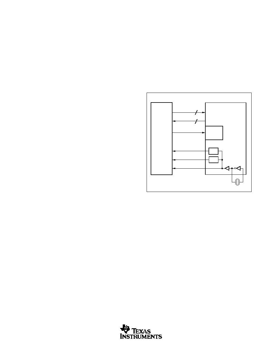
FIGURE 1. AFE1302/DSP Interface.
ADSL DSP
AFE1302
4
TX[0:3]
RX[0:3]
CLWD
CLKNIB
CLKM
CTRLIN
Control
Register
÷
4N
4
÷
N
NOTE: N = 1, 2, 4, 8 set by control register.
To insure that TX distortion and noise do not degrade the
RX downstream performance, external filtering and trans-
hybrid loss of greater than 30dB is required. Refer to
Figure 6 for an external circuit and contract TI for a detailed
reference design document.
DIGITAL DATA TRANSMISSION
Data is transmitted to the AFE1302 from the DSP on the
TX[0:3] lines, as shown in Figure 1. The Data TX[0:3]
changes during the rising edge of CLKM within the DSP,
and the Data are valid on the falling edge of CLKM for the
AFE to read. The minimum setup and hold time are 5ns (see
Figure 2); the start of a new sample is indicated by CLWD
being HIGH.