"20-Bit Universal Bus Driver With 3-State Outputs"
SN74ALVC162836
20-BIT UNIVERSAL BUS DRIVER
WITH 3-STATE OUTPUTS
SCES129B MARCH 1998 REVISED FEBRUARY 1999
1
POST OFFICE BOX 655303
·
DALLAS, TEXAS 75265
D
Member of the Texas Instruments
Widebus
TM
Family
D
EPIC
TM
(Enhanced-Performance Implanted
CMOS) Submicron Process
D
Output Port Has Equivalent 26-
Series
Resistors, So No External Resistors Are
Required
D
Designed to Comply With JEDEC 168-Pin
and 200-Pin SDRAM Buffered DIMM
Specification
D
Package Options Include Plastic Shrink
Small-Outline (DL), Thin Shrink
Small-Outline (DGG), and Thin Very
Small-Outline (DGV) Packages
description
This 20-bit universal bus driver is designed for
1.65-V to 3.6-V V
CC
operation.
Data flow from A to Y is controlled by the
output-enable (OE) input. The device operates in
the transparent mode when the latch-enable (LE)
input is low. When LE is high, the A data is latched
if the clock (CLK) input is held at a high or low logic
level. If LE is high, the A data is stored in the
latch/flip-flop on the low-to-high transition of CLK.
When OE is high, the outputs are in the
high-impedance state.
The output port includes equivalent 26-
series
resistors to reduce overshoot and undershoot.
To ensure the high-impedance state during power
up or power down, OE should be tied to V
CC
through a pullup resistor; the minimum value of
the resistor is determined by the current-sinking
capability of the driver.
The SN74ALVC162836 is characterized for
operation from 40
°
C to 85
°
C.
Copyright
©
1999, Texas Instruments Incorporated
Please be aware that an important notice concerning availability, standard warranty, and use in critical applications of
Texas Instruments semiconductor products and disclaimers thereto appears at the end of this data sheet.
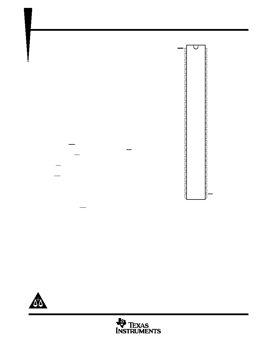
DGG, DGV, OR DL PACKAGE
(TOP VIEW)
1
2
3
4
5
6
7
8
9
10
11
12
13
14
15
16
17
18
19
20
21
22
23
24
25
26
27
28
56
55
54
53
52
51
50
49
48
47
46
45
44
43
42
41
40
39
38
37
36
35
34
33
32
31
30
29
OE
Y1
Y2
GND
Y3
Y4
V
CC
Y5
Y6
Y7
GND
Y8
Y9
Y10
Y11
Y12
Y13
GND
Y14
Y15
Y16
V
CC
Y17
Y18
GND
Y19
Y20
NC
CLK
A1
A2
GND
A3
A4
V
CC
A5
A6
A7
GND
A8
A9
A10
A11
A12
A13
GND
A14
A15
A16
V
CC
A17
A18
GND
A19
A20
LE
NC No internal connection
EPIC and Widebus are trademarks of Texas Instruments Incorporated.
PRODUCTION DATA information is current as of publication date.
Products conform to specifications per the terms of Texas Instruments
standard warranty. Production processing does not necessarily include
testing of all parameters.
SN74ALVC162836
20-BIT UNIVERSAL BUS DRIVER
WITH 3-STATE OUTPUTS
SCES129B MARCH 1998 REVISED FEBRUARY 1999
2
POST OFFICE BOX 655303
·
DALLAS, TEXAS 75265
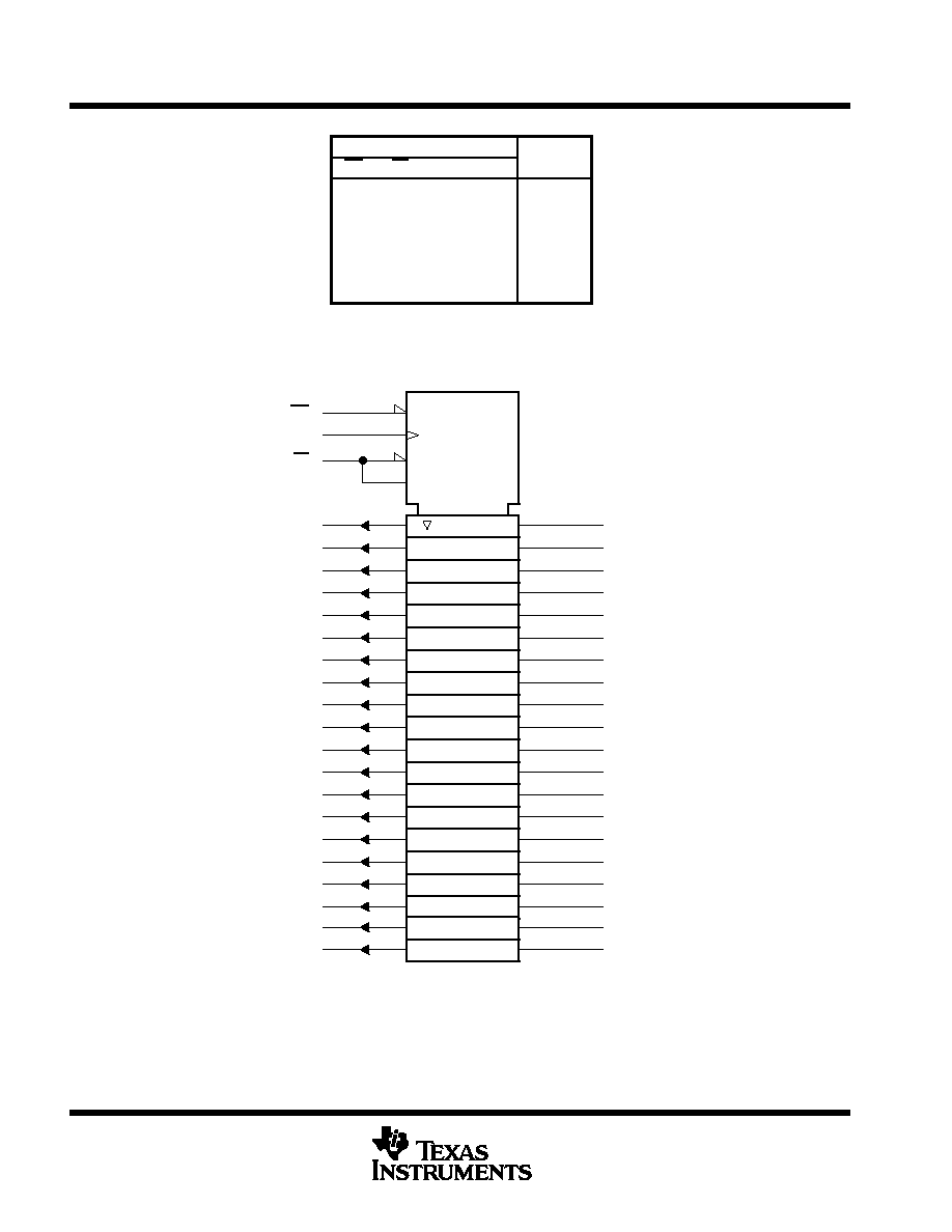
FUNCTION TABLE
INPUTS
OUTPUT
OE
LE
CLK
A
Y
H
X
X
X
Z
L
L
X
L
L
L
L
X
H
H
L
H
L
L
L
H
H
H
L
H
L or H
X
Y0
Output level before the indicated steady-state
input conditions were established
logic symbol
A1
55
A2
54
A3
52
A4
51
A5
49
A6
48
A7
47
A8
45
A9
44
A10
43
A11
42
A12
41
A13
40
A14
38
A15
37
A16
36
A17
34
A18
33
OE
EN1
1
56
CLK
2
Y1
3
Y2
5
Y3
1
6
Y4
8
Y5
9
Y6
10
Y7
12
Y8
13
Y9
14
Y10
15
Y11
16
Y12
17
Y13
19
Y14
20
Y15
21
Y16
23
Y17
24
Y18
C3
29
G2
LE
2C3
1
1
3D
A19
31
A20
30
26
Y19
27
Y20
This symbol is in accordance with ANSI/IEEE Std 91-1984 and IEC Publication 617-12.
SN74ALVC162836
20-BIT UNIVERSAL BUS DRIVER
WITH 3-STATE OUTPUTS
SCES129B MARCH 1998 REVISED FEBRUARY 1999
3
POST OFFICE BOX 655303
·
DALLAS, TEXAS 75265
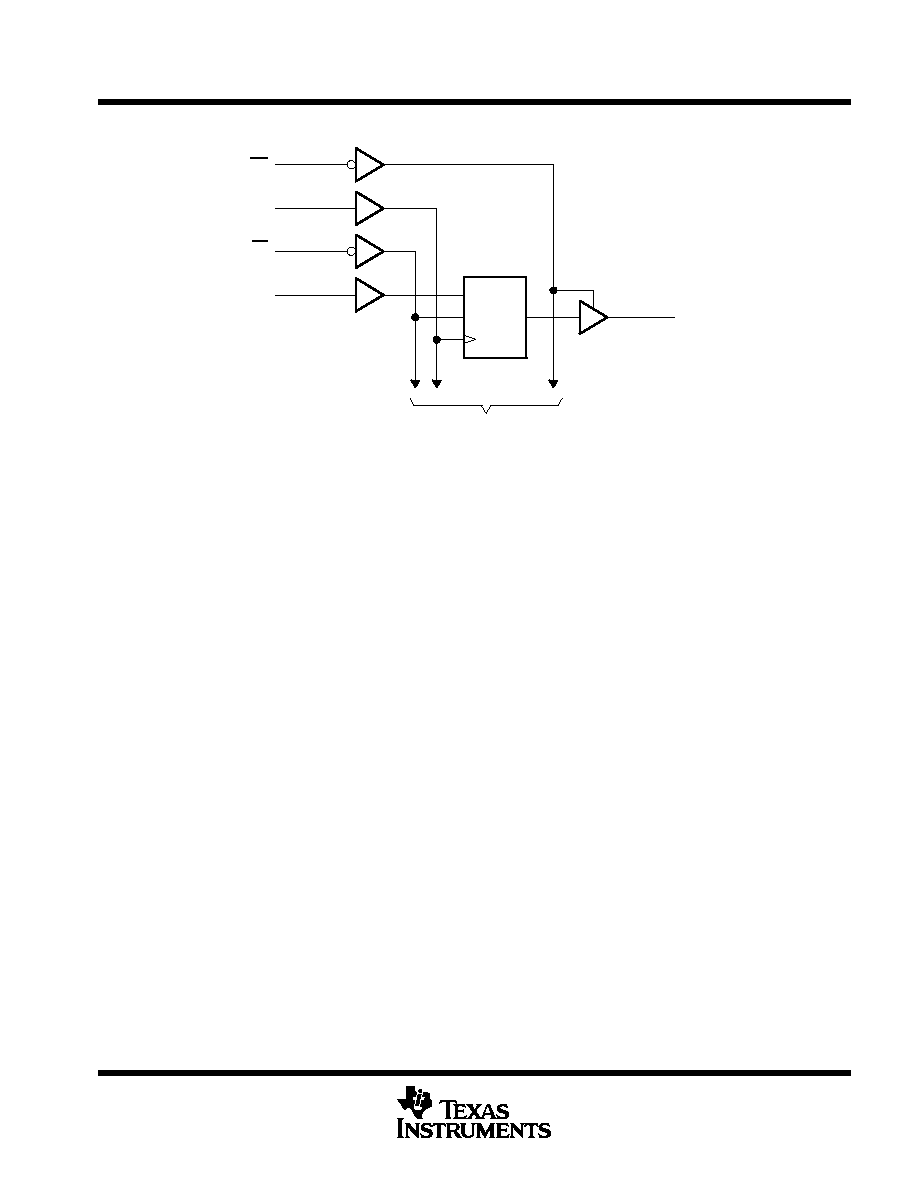
logic diagram (positive logic)
1
56
29
55
1D
C1
CLK
2
To 19 Other Channels
OE
CLK
LE
A1
Y1
absolute maximum ratings over operating free-air temperature range (unless otherwise noted)
Supply voltage range, V
CC
0.5 V to 4.6 V
. . . . . . . . . . . . . . . . . . . . . . . . . . . . . . . . . . . . . . . . . . . . . . . . . . . . . . . . .
Input voltage range, V
I
(see Note 1)
0.5 V to 4.6 V
. . . . . . . . . . . . . . . . . . . . . . . . . . . . . . . . . . . . . . . . . . . . . . . . .
Output voltage range, V
O
(see Notes 1 and 2)
0.5 V to V
CC
+ 0.5 V
. . . . . . . . . . . . . . . . . . . . . . . . . . . . . . . . . .
Input clamp current, I
IK
(V
I
< 0)
50 mA
. . . . . . . . . . . . . . . . . . . . . . . . . . . . . . . . . . . . . . . . . . . . . . . . . . . . . . . . . . .
Output clamp current, I
OK
(V
O
< 0)
50 mA
. . . . . . . . . . . . . . . . . . . . . . . . . . . . . . . . . . . . . . . . . . . . . . . . . . . . . . . .
Continuous output current, I
O
±
50 mA
. . . . . . . . . . . . . . . . . . . . . . . . . . . . . . . . . . . . . . . . . . . . . . . . . . . . . . . . . . . . .
Continuous current through each V
CC
or GND
±
100 mA
. . . . . . . . . . . . . . . . . . . . . . . . . . . . . . . . . . . . . . . . . . . . .
Package thermal impedance,
JA
(see Note 3): DGG package
81
°
C/W
. . . . . . . . . . . . . . . . . . . . . . . . . . . . . . . .
DGV package
86
°
C/W
. . . . . . . . . . . . . . . . . . . . . . . . . . . . . . . .
DL package
74
°
C/W
. . . . . . . . . . . . . . . . . . . . . . . . . . . . . . . . . .
Storage temperature range, T
stg
65
°
C to 150
°
C
. . . . . . . . . . . . . . . . . . . . . . . . . . . . . . . . . . . . . . . . . . . . . . . . . . .
Stresses beyond those listed under "absolute maximum ratings" may cause permanent damage to the device. These are stress ratings only, and
functional operation of the device at these or any other conditions beyond those indicated under "recommended operating conditions" is not
implied. Exposure to absolute-maximum-rated conditions for extended periods may affect device reliability.
NOTES:
1. The input negative-voltage and output voltage ratings may be exceeded if the input and output current ratings are observed.
2. This value is limited to 4.6 V maximum.
3. The package thermal impedance is calculated in accordance with JESD 51.
SN74ALVC162836
20-BIT UNIVERSAL BUS DRIVER
WITH 3-STATE OUTPUTS
SCES129B MARCH 1998 REVISED FEBRUARY 1999
4
POST OFFICE BOX 655303
·
DALLAS, TEXAS 75265
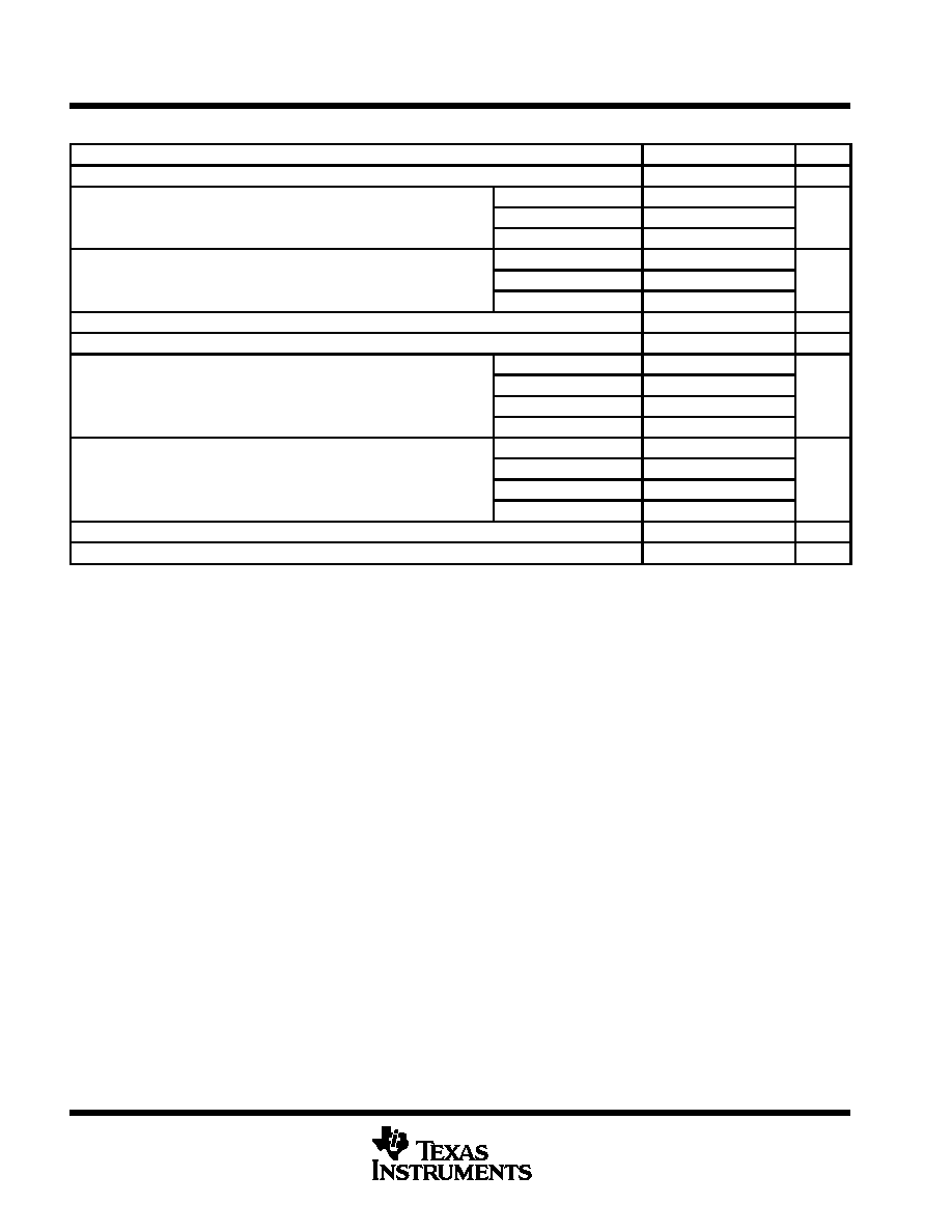
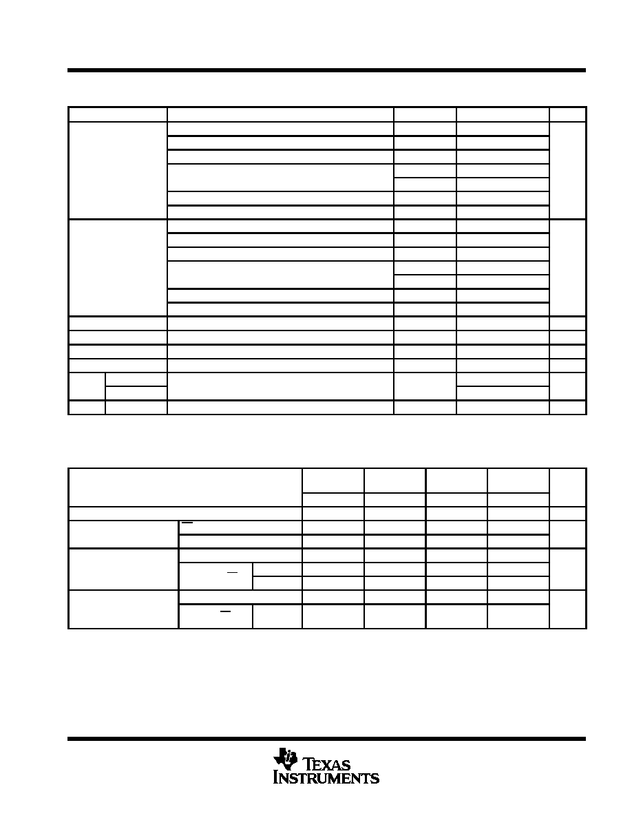
recommended operating conditions (see Note 4)
MIN
MAX
UNIT
VCC
Supply voltage
1.65
3.6
V
VCC = 1.65 V to 1.95 V
0.65
×
VCC
VIH
High-level input voltage
VCC = 2.3 V to 2.7 V
1.7
V
VCC = 2.7 V to 3.6 V
2
VCC = 1.65 V to 1.95 V
0.35
×
VCC
VIL
Low-level input voltage
VCC = 2.3 V to 2.7 V
0.7
V
VCC = 2.7 V to 3.6 V
0.8
VI
Input voltage
0
VCC
V
VO
Output voltage
0
VCC
V
VCC = 1.65 V
2
IOH
High level output current
VCC = 2.3 V
6
mA
IOH
High-level output current
VCC = 2.7 V
8
mA
VCC = 3 V
12
VCC = 1.65 V
2
IOL
Low level output current
VCC = 2.3 V
6
mA
IOL
Low-level output current
VCC = 2.7 V
8
mA
VCC = 3 V
12
t/
v
Input transition rise or fall rate
10
ns/V
TA
Operating free-air temperature
40
85
°
C
NOTE 4: All unused inputs of the device must be held at VCC or GND to ensure proper device operation. Refer to the TI application report,
Implications of Slow or Floating CMOS Inputs, literature number SCBA004.
SN74ALVC162836
20-BIT UNIVERSAL BUS DRIVER
WITH 3-STATE OUTPUTS
SCES129B MARCH 1998 REVISED FEBRUARY 1999
5
POST OFFICE BOX 655303
·
DALLAS, TEXAS 75265
electrical characteristics over recommended operating free-air temperature range (unless
otherwise noted)
PARAMETER
TEST CONDITIONS
VCC
MIN
TYP
MAX
UNIT
IOH = 100
µ
A
1.65 V to 3.6 V
VCC0.2
IOH = 2 mA
1.65 V
1.2
IOH = 4 mA
2.3 V
1.9
VOH
IOH = 6 mA
2.3 V
1.7
V
IOH = 6 mA
3 V
2.4
IOH = 8 mA
2.7 V
2
IOH = 12 mA
3 V
2
IOL = 100
µ
A
1.65 V to 3.6 V
0.2
IOL = 2 mA
1.65 V
0.45
IOL = 4 mA
2.3 V
0.4
VOL
IOL = 6 mA
2.3 V
0.55
V
IOL = 6 mA
3 V
0.55
IOL = 8 mA
2.7 V
0.6
IOL = 12 mA
3 V
0.8
II
VI = VCC or GND
3.6 V
±
5
µ
A
IOZ
VO = VCC or GND
3.6 V
±
10
µ
A
ICC
VI = VCC or GND,
IO = 0
3.6 V
40
µ
A
ICC
One input at VCC 0.6 V,
Other inputs at VCC or GND
3 V to 3.6 V
750
µ
A
Ci
Control inputs
VI = VCC or GND
3 3 V
5
pF
Ci
Data inputs
VI = VCC or GND
3.3 V
5.5
pF
Co
Outputs
VO = VCC or GND
3.3 V
7.5
pF
All typical values are at VCC = 3.3 V, TA = 25
°
C.
timing requirements over recommended operating free-air temperature range (unless otherwise
noted) (see Figures 1 through 3)
VCC = 1.8 V
VCC = 2.5 V
±
0.2 V
VCC = 2.7 V
VCC = 3.3 V
±
0.3 V
UNIT
MIN
MAX
MIN
MAX
MIN
MAX
MIN
MAX
fclock
Clock frequency
150
150
150
MHz
t
Pulse duration
LE low
3.3
3.3
3.3
ns
tw
Pulse duration
CLK high or low
3.3
3.3
3.3
ns
Data before CLK
1.4
1.7
1.5
tsu
Setup time
Data before LE
CLK high
1.2
1.6
1.3
ns
Data before LE
CLK low
1.4
1.5
1.2
Data after CLK
0.9
0.9
0.9
th
Hold time
Data after LE
CLK
high or low
1.1
1.1
1.1
ns
This information was not available at the time of publication.