AM26LS31C, AM26LS31M
QUADRUPLE DIFFERENTIAL LINE DRIVER
SLLS114H ≠ JANUARY 1979 ≠ REVISED JULY 2002
1
POST OFFICE BOX 655303
∑
DALLAS, TEXAS 75265
D
Meets or Exceeds the Requirements of
ANSI TIA/EIA-422-B and ITU
Recommendation V.11
D
Operates From a Single 5-V Supply
D
TTL Compatible
D
Complementary Outputs
D
High Output Impedance in Power-Off
Conditions
D
Complementary Output-Enable Inputs
description/ordering information
The AM26LS31 is a quadruple
complementary-output line driver designed to
meet the requirements of ANSI TIA/EIA-422-B
and ITU (formerly CCITT) Recommendation V.11.
The 3-state outputs have high-current capability
for driving balanced lines such as twisted-pair or
parallel-wire transmission lines, and they are in
the high-impedance state in the power-off
condition. The enable function is common to all
four drivers and offers the choice of an active-high
or active-low enable (G, G) input. Low-power
Schottky circuitry reduces power consumption
without sacrificing speed.
ORDERING INFORMATION
TA
PACKAGE
ORDERABLE
PART NUMBER
TOP-SIDE
MARKING
PDIP ≠ N
Tube
AM26LS31CN
AM26LS31CN
SOIC
D
Tube
AM26LS31CD
AM26LS31C
0
∞
C to 70
∞
C
SOIC ≠ D
Tape and reel
AM26LS31CDR
AM26LS31C
SOP ≠ NS
Tape and reel
AM26LS31CNSR
26LS31
SSOP ≠ DB
Tape and reel
AM26LS31CDBR
SA31C
55
∞
C to 125
∞
C
CDIP ≠ J
Tube
AM26LS31MJ
AM26LS31MJB
≠ 55
∞
C to 125
∞
C
LCCC ≠ FK
Tube
AM26LS31MFK
AM26LS31MFKB
Package drawings, standard packing quantities, thermal data, symbolization, and PCB design guidelines are
available at www.ti.com/sc/package.
Copyright
2002, Texas Instruments Incorporated
PRODUCTION DATA information is current as of publication date.
Products conform to specifications per the terms of Texas Instruments
standard warranty. Production processing does not necessarily include
testing of all parameters.
Please be aware that an important notice concerning availability, standard warranty, and use in critical applications of
Texas Instruments semiconductor products and disclaimers thereto appears at the end of this data sheet.
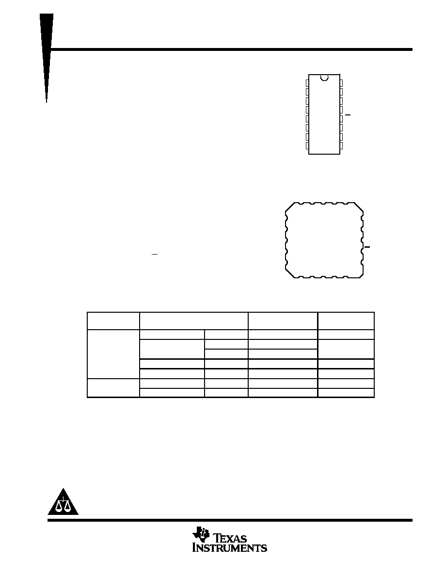
1
2
3
4
5
6
7
8
16
15
14
13
12
11
10
9
1A
1Y
1Z
G
2Z
2Y
2A
GND
V
CC
4A
4Y
4Z
G
3Z
3Y
3A
D, DB, N, NS, OR J PACKAGE
(TOP VIEW)
19
20
1
3
2
17
18
16
15
14
13
12
11
9
10
5
4
6
7
8
4Y
4Z
NC
G
3Z
1Z
G
NC
2Z
2Y
1Y
1A
NC
V
4A
GND
NC
3A
3Y
2A
FK PACKAGE
(TOP VIEW)
CC
On products compliant to MIL-PRF-38535, all parameters are tested
unless otherwise noted. On all other products, production
processing does not necessarily include testing of all parameters.
AM26LS31C, AM26LS31M
QUADRUPLE DIFFERENTIAL LINE DRIVER
SLLS114H ≠ JANUARY 1979 ≠ REVISED JULY 2002
2
POST OFFICE BOX 655303
∑
DALLAS, TEXAS 75265
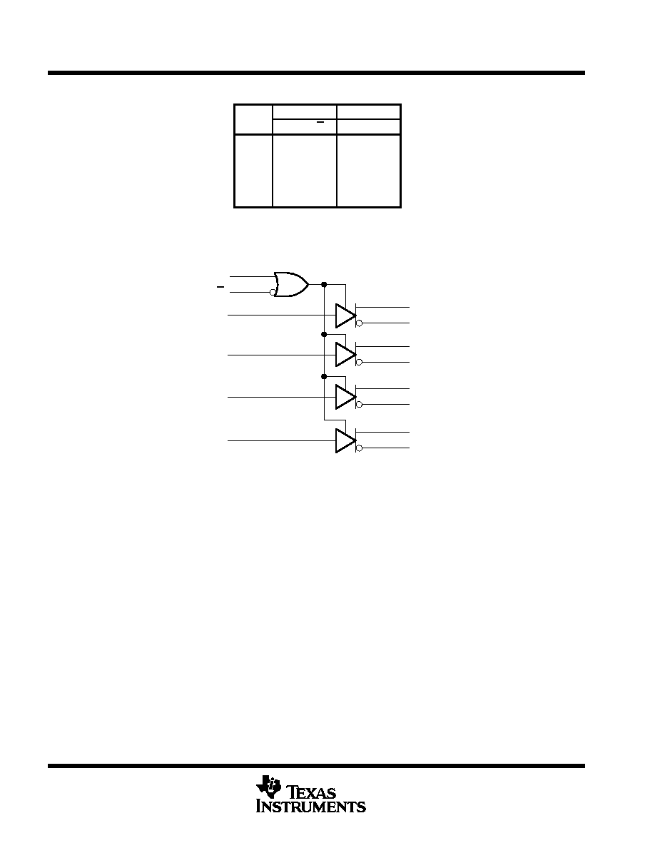
FUNCTION TABLE
(each driver)
INPUT
ENABLES
OUTPUTS
A
G
G
Y
Z
H
H
X
H
L
L
H
X
L
H
H
X
L
H
L
L
X
L
L
H
X
L
H
Z
Z
H = high level, L = low level, X = irrelevant,
Z = high impedance (off)
logic diagram (positive logic)
1Z
1Y
G
G
1A
4
12
1
2
3
2Z
2Y
2A
7
6
5
3Z
3Y
3A
9
10
11
4Z
4Y
4A
15
14
13
AM26LS31C, AM26LS31M
QUADRUPLE DIFFERENTIAL LINE DRIVER
SLLS114H ≠ JANUARY 1979 ≠ REVISED JULY 2002
3
POST OFFICE BOX 655303
∑
DALLAS, TEXAS 75265
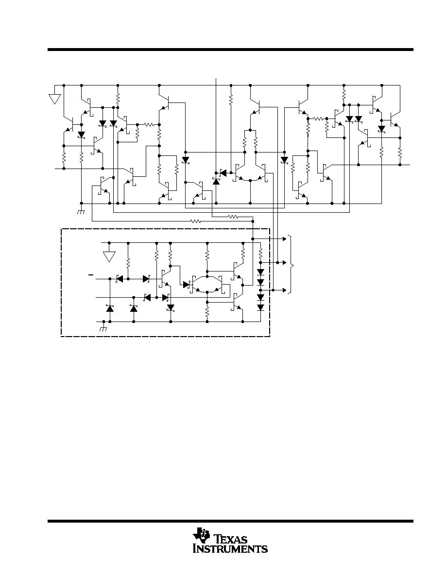
schematic (each driver)
22 k
To Three Other Drivers
Common to All Four Drivers
GND
Enable G
Enable G
VCC
V
V
Output Y
9
Input A
22 k
22 k
All resistor values are nominal.
Output Z
9
AM26LS31C, AM26LS31M
QUADRUPLE DIFFERENTIAL LINE DRIVER
SLLS114H ≠ JANUARY 1979 ≠ REVISED JULY 2002
4
POST OFFICE BOX 655303
∑
DALLAS, TEXAS 75265
absolute maximum ratings over operating free-air temperature range (unless otherwise noted)
Supply voltage, V
CC
(see Note 1)
7 V
. . . . . . . . . . . . . . . . . . . . . . . . . . . . . . . . . . . . . . . . . . . . . . . . . . . . . . . . . . . . .
Input voltage, V
I
7 V
. . . . . . . . . . . . . . . . . . . . . . . . . . . . . . . . . . . . . . . . . . . . . . . . . . . . . . . . . . . . . . . . . . . . . . . . . . . .
Output off-state voltage
5.5 V
. . . . . . . . . . . . . . . . . . . . . . . . . . . . . . . . . . . . . . . . . . . . . . . . . . . . . . . . . . . . . . . . . . . .
Package thermal impedance,
JA
(see Note 2): D package
73
∞
C/W
. . . . . . . . . . . . . . . . . . . . . . . . . . . . . . . . . . .
DB package
82
∞
C/W
. . . . . . . . . . . . . . . . . . . . . . . . . . . . . . . . .
N package
67
∞
C/W
. . . . . . . . . . . . . . . . . . . . . . . . . . . . . . . . . . .
NS package
64
∞
C/W
. . . . . . . . . . . . . . . . . . . . . . . . . . . . . . . . .
Lead temperature 1,6 mm (1/16 inch) from case for 10 seconds
260
∞
C
. . . . . . . . . . . . . . . . . . . . . . . . . . . . . . .
Lead temperature 1,6 mm (1/16 inch) from case for 60 seconds: J package
300
∞
C
. . . . . . . . . . . . . . . . . . . . .
Storage temperature range, T
stg
≠65
∞
C to 150
∞
C
. . . . . . . . . . . . . . . . . . . . . . . . . . . . . . . . . . . . . . . . . . . . . . . . . . .
Stresses beyond those listed under "absolute maximum ratings" may cause permanent damage to the device. These are stress ratings only, and
functional operation of the device at these or any other conditions beyond those indicated under "recommended operating conditions" is not
implied. Exposure to absolute-maximum-rated conditions for extended periods may affect device reliability.
NOTES:
1. All voltage values, except differential output voltage VOD, are with respect to network GND.
2. The package thermal impedance is calculated in accordance with JESD 51-7.
DISSIPATION RATING TABLE
PACKAGE
TA
25
∞
C
DERATING FACTOR
TA = 70
∞
C
TA = 125
∞
C
PACKAGE
A
POWER RATING
ABOVE TA = 25
∞
C
A
POWER RATING
A
POWER RATING
FK
1375 mW
11.0 mW/
∞
C
880 mW
275 mW
J
1375 mW
11.0 mW/
∞
C
880 mW
275 mW
This is the inverse of the traditional junction-to-ambient thermal resistance (R
JA). Thermal resistances are not
production tested and the values given are for informational purposes only.
recommended operating conditions
MIN
NOM
MAX
UNIT
VCC
Supply voltage
AM26LS31C
4.75
5
5.25
V
VCC
Supply voltage
AM26LS31M
4.5
5
5.5
V
VIH
High-level input voltage
2
V
VIL
Low-level input voltage
0.8
V
IOH
High-level output current
≠20
mA
IOL
Low-level output current
20
mA
TA
Operating free air temperature
AM26LS31C
0
70
∞
C
TA
Operating free-air temperature
AM26LS31M
≠55
125
∞
C
AM26LS31C, AM26LS31M
QUADRUPLE DIFFERENTIAL LINE DRIVER
SLLS114H ≠ JANUARY 1979 ≠ REVISED JULY 2002
5
POST OFFICE BOX 655303
∑
DALLAS, TEXAS 75265
electrical characteristics over operating free-air temperature range (unless otherwise noted)
PARAMETER
TEST CONDITIONS
MIN
TYP
MAX
UNIT
VIK
Input clamp voltage
VCC = MIN,
II = ≠18 mA
≠1.5
V
VOH
High level output voltage
VCC = MIN,
TA = ≠55
∞
C
2.4
V
VOH
High-level output voltage
CC
,
IOH = ≠20 mA
All other temperatures
2.5
V
VOL
Low-level output voltage
VCC = MIN,
IOL = 20 mA
0.5
V
IOZ
Off state (high impedance state) output current
VCC = MIN
VO = 0.5 V
≠20
µ
A
IOZ
Off-state (high-impedance-state) output current
VCC = MIN
VO = 2.5 V
20
µ
A
II
Input current at maximum input voltage
VCC = MAX,
VI = 7 V
0.1
mA
IIH
High-level input current
VCC = MAX,
VI = 2.7 V
20
µ
A
IIL
Low-level input current
VCC = MAX,
VI = 0.4 V
≠0.36
mA
IOS
Short-circuit output currentß
VCC = MAX
≠30
≠150
mA
ICC
Supply current
VCC = MAX,
All outputs disabled
32
80
mA
For C suffix devices, VCC MIN = 4.75 V and VCC MAX = 5.25 V. For M suffix devices, VCC MIN = 4.5 V and VCC MAX = 5.5 V.
All typical values are at VCC = 5 V and TA = 25
∞
C.
ß Not more than one output should be shorted at a time, and duration of the short circuit should not exceed one second.
switching characteristics, V
CC
= 5 V, T
A
= 25
∞
C (see Figure 1)
PARAMETER
TEST CONDITIONS
MIN
TYP
MAX
UNIT
tPLH
Propagation delay time, low-to-high-level output
CL = 30 pF
S1 and S2 open
14
20
ns
tPHL
Propagation delay time, high-to-low-level output
CL = 30 pF,
S1 and S2 open
14
20
ns
tPZH
Output enable time to high level
CL = 30 pF
RL = 75
25
40
ns
tPZL
Output enable time to low level
CL = 30 pF
RL = 180
37
45
ns
tPHZ
Output disable time from high level
CL = 10 pF
S1 and S2 closed
21
30
ns
tPLZ
Output disable time from low level
CL = 10 pF,
S1 and S2 closed
23
35
ns
Output-to-output skew
CL = 30 pF,
S1 and S2 open
1
6
ns