 | ÐлекÑÑоннÑй компоненÑ: AM26LV31 | СкаÑаÑÑ:  PDF PDF  ZIP ZIP |
Äîêóìåíòàöèÿ è îïèñàíèÿ www.docs.chipfind.ru
AM26LV31
LOW-VOLTAGE HIGH-SPEED
QUADRUPLE DIFFERENTIAL LINE DRIVER
SLLS201E MAY 1995 REVISED DECEMBER 1999
1
POST OFFICE BOX 655303
·
DALLAS, TEXAS 75265
D
Switching Rates up to 32 MHz
D
Operates From a Single 3.3-V Supply
D
Propagation Delay Time . . . 8 ns Typ
D
Pulse Skew Time . . . 500 ps Typ
D
High Output-Drive Current . . .
±
30 mA
D
Controlled Rise and Fall Times . . . 3 ns Typ
D
Differential Output Voltage With
100-
Load . . . 1.5 V Typ
D
Ultra-Low Power Dissipation
dc, 0.3 mW Max
32 MHz All Channels (No Load),
385 mW Typ
D
Accepts 5-V Logic Inputs With a 3.3-V
Supply
D
Low-Voltage Pin-to-Pin Compatible
Replacement for AM26C31, AM26LS31,
MB571
D
High Output Impedance in Power-Off
Condition
D
Driver Output Short-Protection Circuit
D
Package Options Include Plastic
Small-Outline (D, NS) Packages
description
The AM26LV31 is a BiCMOS quadruple differential line driver with 3-state outputs. It is designed to be similar
to TIA/EIA-422-B and ITU Recommendation V.11 drivers with reduced supply-voltage range.
The device is optimized for balanced-bus transmission at switching rates up to 32 MHz. The outputs have very
high current capability for driving balanced lines such as twisted-pair transmission lines and provide a high
impedance in the power-off condition. The enable function is common to all four drivers and offers the choice
of active-high or active-low enable inputs. The AM26LV31 is designed using Texas Instruments (TI
TM
)
proprietary LinIMPACT-C60
TM
technology, facilitating ultra-low power consumption without sacrificing speed.
This device offers optimum performance when used with the AM26LV32 quadruple line receivers.
The AM26LV31C is characterized for operation from 0
°
C to 70
°
C.
FUNCTION TABLE
INPUT
ENABLES
OUTPUTS
A
G
G
Y
Z
H
H
X
H
L
L
H
X
L
H
H
X
L
H
L
L
X
L
L
H
X
L
H
Z
Z
H = high level, L = low level, X = irrelevant,
Z = high impedance (off)
Copyright
©
1999, Texas Instruments Incorporated
PRODUCTION DATA information is current as of publication date.
Products conform to specifications per the terms of Texas Instruments
standard warranty. Production processing does not necessarily include
testing of all parameters.
LinIMPACT-C60 and TI are trademarks of Texas Instruments Incorporated.
Please be aware that an important notice concerning availability, standard warranty, and use in critical applications of
Texas Instruments semiconductor products and disclaimers thereto appears at the end of this data sheet.
1
2
3
4
5
6
7
8
16
15
14
13
12
11
10
9
1A
1Y
1Z
G
2Z
2Y
2A
GND
V
CC
4A
4Y
4Z
G
3Z
3Y
3A
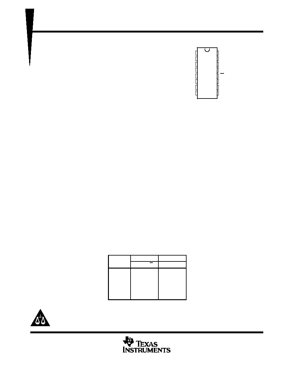
D OR NS PACKAGE
(TOP VIEW)
The D package is available taped
and reeled. The NS package is only
available taped and reeled. Add the
suffix R to device type (e.g.,
AM26LV31CDR).
AM26LV31
LOW-VOLTAGE HIGH-SPEED
QUADRUPLE DIFFERENTIAL LINE DRIVER
SLLS201E MAY 1995 REVISED DECEMBER 1999
2
POST OFFICE BOX 655303
·
DALLAS, TEXAS 75265
logic symbol
1
EN
This symbol is in accordance with ANSI/IEEE Std 91-1984 and
IEC Publication 617-12.
G
4
G
12
G
1
1A
1Y
2
1Z
3
2Y
6
2Z
5
3Y
10
3Z
11
4Y
14
4Z
13
7
2A
9
3A
15
4A
logic diagram (positive logic)
4Z
4Y
3Z
3Y
2Z
2Y
1Z
1Y
13
14
11
10
5
6
3
2
4A
3A
2A
1A
G
G
15
9
7
1
12
4
schematic (each driver)
Input
VCC
TYPICAL OF ALL OUTPUTS (Y AND Z)
Output
VCC
GND
GND
EQUIVALENT OF EACH INPUT (A, G, OR G)
100
40 k
6
All resistor values are nominal.
AM26LV31
LOW-VOLTAGE HIGH-SPEED
QUADRUPLE DIFFERENTIAL LINE DRIVER
SLLS201E MAY 1995 REVISED DECEMBER 1999
3
POST OFFICE BOX 655303
·
DALLAS, TEXAS 75265
absolute maximum ratings over operating free-air temperature range (unless otherwise noted)
Supply voltage range, V
CC
(see Note 1)
0.3 V to 6 V
. . . . . . . . . . . . . . . . . . . . . . . . . . . . . . . . . . . . . . . . . . . . . .
Input voltage range, V
I
0.3 V to 6 V
. . . . . . . . . . . . . . . . . . . . . . . . . . . . . . . . . . . . . . . . . . . . . . . . . . . . . . . . . . . . . .
Output voltage range, V
O
0.3 V to 6 V
. . . . . . . . . . . . . . . . . . . . . . . . . . . . . . . . . . . . . . . . . . . . . . . . . . . . . . . . . . .
Package thermal impedance,
JA
(see Note 2): D package
73
°
C/W
. . . . . . . . . . . . . . . . . . . . . . . . . . . . . . . . . . .
NS package
64
°
C/W
. . . . . . . . . . . . . . . . . . . . . . . . . . . . . . . . .
Storage temperature range, T
stg
65
°
C to 150
°
C
. . . . . . . . . . . . . . . . . . . . . . . . . . . . . . . . . . . . . . . . . . . . . . . . . . .
Lead temperature 1,6 mm (1/16 inch) from case for 10 seconds
260
°
C
. . . . . . . . . . . . . . . . . . . . . . . . . . . . . . .
Stresses beyond those listed under "absolute maximum ratings" may cause permanent damage to the device. These are stress ratings only, and
functional operation of the device at these or any other conditions beyond those indicated under "recommended operating conditions" is not
implied. Exposure to absolute-maximum-rated conditions for extended periods may affect device reliability.
NOTES:
1. All voltage values are with respect to GND.
2. The package thermal impedance is calculated in accordance with JESD 51.
recommended operating conditions
MIN
NOM
MAX
UNIT
Supply voltage, VCC
3
3.3
3.6
V
High-level input voltage, VIH
2
V
Low-level input voltage, VIL
0.8
V
High-level output current, IOH
30
mA
Low-level output current, IOL
30
mA
Operating free-air temperature, TA
0
70
°
C
AM26LV31
LOW-VOLTAGE HIGH-SPEED
QUADRUPLE DIFFERENTIAL LINE DRIVER
SLLS201E MAY 1995 REVISED DECEMBER 1999
4
POST OFFICE BOX 655303
·
DALLAS, TEXAS 75265
electrical characteristics over recommended operating supply-voltage and free-air temperature
ranges (unless otherwise noted)
PARAMETER
TEST CONDITIONS
MIN
TYP
MAX
UNIT
VIK
Input clamp voltage
II = 18 mA
1.5
V
VOH
High-level output voltage
VIH = 2 V,
IOH = 12 mA
1.85
2.3
V
VOL
Low-level output voltage
VIL = 0.8 V,
IOH = 12 mA
0.8
1.05
V
|VOD|
Differential output voltage
0.95
1.5
V
VOC
Common-mode output voltage
RL = 100
1.3
1.55
1.8
V
|VOC|
Change in magnitude of
common-mode output voltage
RL = 100
±
0.2
V
IO
Output current with power off
VO = 0.25 V or 6 V,
VCC = 0
±
100
µ
A
IOZ
Off-state (high-impedance state)
output current
VO = 0.25 V or 6 V,
G = 0.8 V or G = 2 V
±
100
µ
A
IIH
High-level input current
VCC = 0 or 3 V,
VI = 5.5 V
10
µ
A
IIL
Low-level input current
VCC = 3.6 V,
VI = 0
10
µ
A
IOS
Short-circuit output current
VCC = 3.6 V,
VO = 0
200
mA
ICC
Supply current (all drivers)
VI = VCC or GND,
No load
100
µ
A
Cpd
Power dissipation capacitance (all drivers)§
No load
160
pF
All typical values are at VCC = 3.3 V and TA = 25
°
C.
|VOD| and
|VOC| are the changes in magnitude of VOD and VOC, respectively, that occur when the input is changed from a high level to a low
level.
§ Cpd determines the no-load dynamic current consumption. IS = Cpd
×
VCC
×
f + ICC
switching characteristics, V
CC
= 3.3 V, T
A
= 25
°
C
PARAMETER
TEST CONDITIONS
MIN
TYP
MAX
UNIT
tPLH
Propagation delay time, low- to high-level output
4
8
12
ns
tPHL
Propagation delay time, high- to low-level output
See Figure 2
4
8
12
ns
tt
Transition time (tr or tf)
3
ns
SR
Slew rate, single-ended output voltage
See Note 3 and Figure 2
0.3
1
V/ns
tPZH
Output-enable time to high level
See Figure 3
10
20
ns
tPZL
Output-enable time to low level
See Figure 4
10
20
ns
tPHZ
Output-disable time from high level
See Figure 3
10
20
ns
tPLZ
Output-disable time from low level
See Figure 4
10
20
ns
tsk(p)
Pulse skew
f = 32 MHz,
See Note 4
0.5
1.5
ns
tsk(o)
Skew limit
f = 32 MHz,
See Note 5
1.5
ns
tsk(lim)
Skew limit (device to device)
f = 32 MHz,
See Note 6
3
ns
NOTES:
3. Slew rate is defined by:
SR
+
90% V
OH
*
V
OL
*
10% V
OH
*
V
OL
t
r
, the differential slew rate of V
OD
is 2
SR.
4. Pulse skew is defined as the |tPLH tPHL| of each channel of the same device.
5. Skew limit is the difference between any two outputs of the same device switching in the same direction.
6. Skew limit (device to device) is the maximum difference in propagation delay times between any two channels of any two devices.
AM26LV31
LOW-VOLTAGE HIGH-SPEED
QUADRUPLE DIFFERENTIAL LINE DRIVER
SLLS201E MAY 1995 REVISED DECEMBER 1999
5
POST OFFICE BOX 655303
·
DALLAS, TEXAS 75265
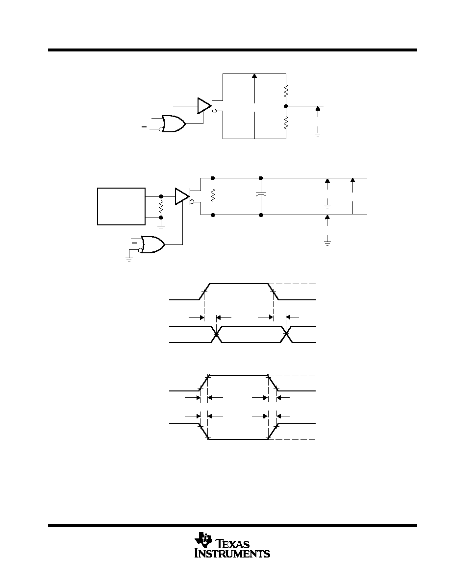
PARAMETER MEASUREMENT INFORMATION
RL/2
VOC
RL/2
VOD2
G
G
A
Y
Z
Figure 1. Differential and Common-Mode Output Voltages
TEST CIRCUIT
Generator
(see Note B)
50
VCC
RL = 100
CL = 15 pF
(see Note A)
VOD
G
G
A
Y
Z
VO
VO
Z
Output, VO
Input
tPLH
tPHL
VCC
0 V
50%
50%
PROPAGATION DELAY TIMES
Y
A
Output, VO
tr
tf
VOH
90%
90%
RISE AND FALL TIMES
10%
10%
VOL
NOTES: A. CL includes probe and jig capacitance.
B. The input pulse is supplied by a generator having the following characteristics: PRR = 32 MHz, ZO
50
, 50% duty cycle,
tr and tf
2 ns.
10%
10%
90%
90%
Y
Z
tf
tr
VOL
VOH
Figure 2. Test Circuit and Voltage Waveforms, t
PHL
and t
PLH