www.ti.com
FEATURES
1
2
3
4
5
6
7
8
16
15
14
13
12
11
10
9
1A
1Y
1Z
G
2Z
2Y
2A
GND
V
CC
4A
4Y
4Z
G
3Z
3Y
3A
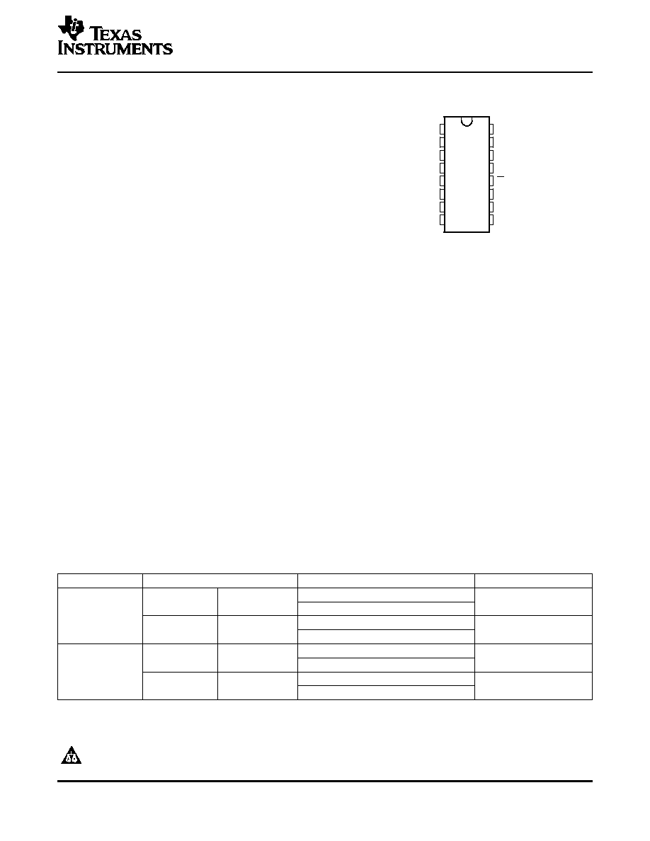
D OR NS PACKAGE
(TOP VIEW)
DESCRIPTION/ORDERING INFORMATION
AM26LV31C, AM26LV31I
LOW-VOLTAGE HIGH-SPEED QUADRUPLE DIFFERENTIAL LINE DRIVERS
SLLS201G ≠ MAY 1995 ≠ REVISED MAY 2005
∑
Switching Rates up to 32 MHz
∑
Operate From a Single 3.3-V Supply
∑
Propagation Delay Time . . . 8 ns Typ
∑
Pulse Skew Time . . . 500 ps Typ
∑
High Output-Drive Current . . .
±
30 mA
∑
Controlled Rise and Fall Times . . . 3 ns Typ
∑
Differential Output Voltage With 100-
Load . . . 1.5 V Typ
∑
Ultra-Low Power Dissipation
≠ dc, 0.3 mW Max
≠ 32 MHz All Channels (No Load), 385 mW Typ
∑
Accept 5-V Logic Inputs With 3.3-V Supply
∑
Low-Voltage Pin-to-Pin Compatible
Replacement for AM26C31, AM26LS31, MB571
∑
High Output Impedance in Power-Off
Condition
∑
Driver Output Short-Protection Circuit
∑
Package Options Include Plastic
Small-Outline (D, NS) Packages
The AM26LV31C and AM26LV31I are BiCMOS quadruple differential line drivers with 3-state outputs. They are
designed to be similar to TIA/EIA-422-B and ITU Recommendation V.11 drivers with reduced supply-voltage
range.
The devices are optimized for balanced-bus transmission at switching rates up to 32 MHz. The outputs have very
high current capability for driving balanced lines such as twisted-pair transmission lines and provide a high
impedance in the power-off condition. The enable function is common to all four drivers and offers the choice of
active-high or active-low enable inputs. The AM26LV31C and AM26LV31I are designed using Texas Instruments
proprietary LinIMPACT-C60TM technology, facilitating ultra-low power consumption without sacrificing speed.
These devices offer optimum performance when used with the AM26LV32 quadruple line receivers.
The AM26LV31C is characterized for operation from 0
∞
C to 70
∞
C. The AM26LV31I is characterized for operation
from ≠45
∞
C to 85
∞
C
ORDERING INFORMATION
T
A
PACKAGE
(1)
ORDERABLE PART NUMBER
TOP-SIDE MARKING
AM26LV31CD
SOIC ≠ D
Tape and reel
AM26LV31C
AM26LV31CDR
0
∞
C to 70
∞
C
AM26LV31CNS
SOIC ≠ NS
Tape and reel
26LV31
AM26LV31CNSR
AM26LV31ID
SOIC ≠ D
Tape and reel
AM26LV31I
AM26LV31IDR
≠45
∞
C to 85
∞
C
AM26LV31INS
SOIC ≠ NS
Tape and reel
26LV31I
AM26LV31INSR
(1)
Package drawings, standard packing quantities, thermal data, symbolization, and PCB design guidelines are available at
www.ti.com/sc/package.
Please be aware that an important notice concerning availability, standard warranty, and use in critical applications of Texas
Instruments semiconductor products and disclaimers thereto appears at the end of this data sheet.
LinIMPACT-C60 is a trademark of Texas Instruments.
PRODUCTION DATA information is current as of publication date.
Copyright © 1995≠2005, Texas Instruments Incorporated
Products conform to specifications per the terms of the Texas
Instruments standard warranty. Production processing does not
necessarily include testing of all parameters.
www.ti.com
4Z
4Y
3Z
3Y
2Z
2Y
1Z
1Y
13
14
11
10
5
6
3
2
4A
3A
2A
1A
G
G
15
9
7
1
12
4
Input
V
CC
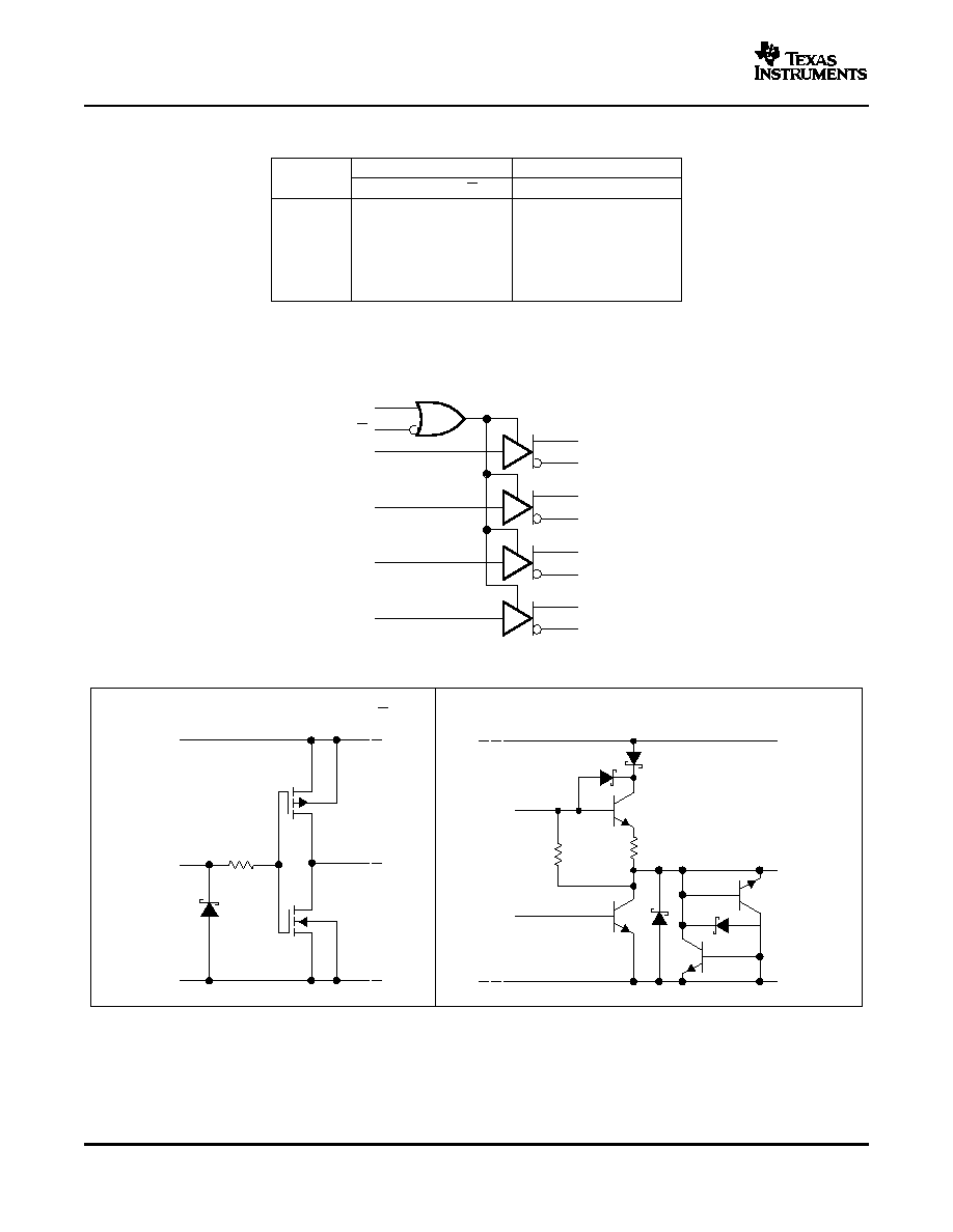
TYPICAL OF ALL OUTPUTS (Y AND Z)
Output
V
CC
GND
GND
EQUIVALENT OF EACH INPUT (A, G, OR G)
100
40 k
6
All resistor values are nominal.
AM26LV31C, AM26LV31I
LOW-VOLTAGE HIGH-SPEED QUADRUPLE DIFFERENTIAL LINE DRIVERS
SLLS201G ≠ MAY 1995 ≠ REVISED MAY 2005
FUNCTION TABLE
(1)
ENABLES
OUTPUTS
INPUT
A
G
G
Y
Z
H
H
X
H
L
L
H
X
L
H
H
X
L
H
L
L
X
L
L
H
X
L
H
Z
Z
(1)
H = high level, L = low level, X = irrelevant,
Z = high impedance (off)
LOGIC DIAGRAM (POSITIVE LOGIC)
SCHEMATIC (EACH DRIVER)
2
www.ti.com
Absolute Maximum Ratings
(1)
Recommended Operating Conditions
Electrical Characteristics
AM26LV31C, AM26LV31I
LOW-VOLTAGE HIGH-SPEED QUADRUPLE DIFFERENTIAL LINE DRIVERS
SLLS201G ≠ MAY 1995 ≠ REVISED MAY 2005
over operating free-air temperature range (unless otherwise noted)
MIN
MAX
UNIT
V
CC
Supply voltage range
(2)
≠0.3
6
V
V
I
Input voltage range
≠0.3
6
V
V
O
Output voltage range
≠0.3
6
V
D package
73
JA
Package thermal impedance
(3)
∞C/W
NS package
64
Lead temperature
1,6 mm (1/16 in) from case for 10 s
260
∞C
T
stg
Storage temperature range
≠65
150
∞C
(1)
Stresses beyond those listed under "absolute maximum ratings" may cause permanent damage to the device. These are stress ratings
only, and functional operation of the device at these or any other conditions beyond those indicated under "recommended operating
conditions" is not implied. Exposure to absolute-maximum-rated conditions for extended periods may affect device reliability.
(2)
All voltage values are with respect to GND.
(3)
The package thermal impedance is calculated in accordance with JESD 51-7.
MIN
NOM
MAX
UNIT
V
CC
Supply voltage
3
3.3
3.6
V
V
IH
High-level input voltage
2
V
V
IL
Low-level input voltage
0.8
V
I
OH
High-level output current
≠30
mA
I
OL
Low-level output current
30
mA
AM26LV31C
0
70
T
A
Operating free-air temperature
∞C
AM26LV31I
≠45
85
over recommended operating supply-voltage and free-air temperature ranges (unless otherwise noted)
PARAMETER
TEST CONDITIONS
MIN
TYP
(1)
MAX
UNIT
V
IK
Input clamp voltage
I
I
= 18 mA
≠1.5
V
V
OH
High-level output voltage
V
IH
= 2 V,
I
OH
= ≠12 mA
1.85
2.3
V
V
OL
Low-level output voltage
V
IL
= 0.8 V,
I
OH
= 12 mA
0.8
1.05
V
|V
OD
|
Differential output voltage
(2)
0.95
1.5
V
V
OC
Common-mode output voltage
1.3
1.55
1.8
V
R
L
= 100
Change in magnitude of
|V
OC
|
±
0.2
V
common-mode output voltage
(2)
I
O
Output current with power off
V
O
= ≠0.25 V or 6 V,
V
CC
= 0
±
100
µ
A
Off-state (high-impedance state)
I
OZ
V
O
= ≠0.25 V or 6 V,
G = 0.8 V or G = 2 V
±
100
µ
A
output current
I
H
High-level input current
V
CC
= 0 or 3 V,
V
I
= 5.5 V
10
µ
A
I
L
Low-level input current
V
CC
= 3.6 V,
V
I
= 0
≠10
µ
A
I
OS
Short-circuit output current
V
CC
= 3.6 V,
V
O
= 0
≠200
mA
I
CC
Supply current (all drivers)
V
I
= V
CC
or GND,
No load
100
µ
A
Power-dissipation capacitance
C
pd
No load
160
pF
(all drivers)
(3)
(1)
All typical values are at V
CC
= 3.3 V, T
A
= 25∞C.
(2)
|V
OD
| and
|V
OC
| are the changes in magnitude of V
OD
and V
OC
, respectively, that occur when the input is changed from a high level to
a low level.
(3)
C
pd
determines the no-load dynamic current consumption. I
S
= C
pd
◊
V
CC
◊
f + I
CC
3
www.ti.com
SR
+
90% V
OH
*
V
OL
*
10% V
OH
*
V
OL
t
r
, the differential slew rate of V
OD
is 2
SR.
Switching Characteristics
AM26LV31C, AM26LV31I
LOW-VOLTAGE HIGH-SPEED QUADRUPLE DIFFERENTIAL LINE DRIVERS
SLLS201G ≠ MAY 1995 ≠ REVISED MAY 2005
V
CC
= 3.3 V, T
A
= 25
∞
C
PARAMETER
TEST CONDITIONS
MIN
TYP
(1)
MAX
UNIT
t
PLH
Propagation delay time, low- to high-level output
See Figure 2
4
8
12
ns
t
PHL
Propagation delay time, high- to low-level output
4
8
12
ns
t
t
Transition time (t
r
or t
f
)
3
ns
SR
Slew rate, single-ended output voltage
See Note
(2)
and Figure 2
0.3
1
V/ns
t
PZH
Output-enable time to high level
See Figure 3
10
20
ns
t
PZL
Output-enable time to low level
See Figure 4
10
20
ns
t
PHZ
Output-disable time from high level
See Figure 3
10
20
ns
t
PLZ
Output-disable time from low level
See Figure 4
10
20
ns
t
sk(p)
Pulse skew
f = 32 MHz,
See Note
(3)
0.5
1.5
ns
t
sk(o)
Skew limit
f = 32 MHz
1.5
ns
t
sk(lim)
Skew limit (device to device)
f = 32 MHz,
See Note
(4)
3
ns
(1)
All typical values are at V
CC
= 3.3 V, T
A
= 25∞C.
(2)
Slew rate is defined by:
(3)
Pulse skew is defined as the |t
PLH
- t
PHL
| of each channel of the same device.
(4)
Skew limit (device to device) is the maximum difference in propagation delay times between any two channels of any two devices.
4
www.ti.com
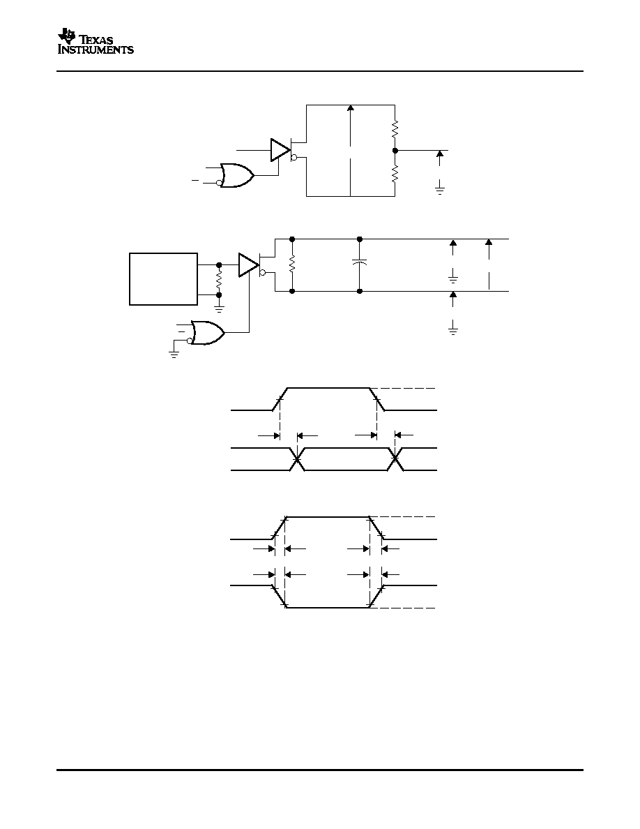
PARAMETER MEASUREMENT INFORMATION
R
L
/2
V
OC
R
L
/2
V
OD2
G
G
A
Y
Z
TEST CIRCUIT
Generator
(see Note B)
50
V
CC
R
L
= 100
C
L
= 15 pF
(see Note A)
V
OD
G
G
A
Y
Z
V
O
V
O
Z
Output, V
O
Input
t
PLH
t
PHL
V
CC
0 V
50%
50%
PROPAGATION DELAY TIMES
Y
A
Output, V
O
t
r
t
f
V
OH
90%
90%
RISE AND FALL TIMES
10%
10%
V
OL
NOTES: A. C
L
includes probe and jig capacitance.
B. The input pulse is supplied by a generator having the following characteristics: PRR = 32 MHz, Z
O
50
, 50% duty cycle,
t
r
and t
f
2 ns.
10%
10%
90%
90%
Y
Z
t
f
t
r
V
OL
V
OH
AM26LV31C, AM26LV31I
LOW-VOLTAGE HIGH-SPEED QUADRUPLE DIFFERENTIAL LINE DRIVERS
SLLS201G ≠ MAY 1995 ≠ REVISED MAY 2005
Figure 1. Differential and Common-Mode Output Voltages
Figure 2. Test Circuit and Voltage Waveforms, t
PHL
and t
PLH
5