 | –≠–ª–µ–∫—Ç—Ä–æ–Ω–Ω—ã–π –∫–æ–º–ø–æ–Ω–µ–Ω—Ç: AM26S10CD | –°–∫–∞—á–∞—Ç—å:  PDF PDF  ZIP ZIP |
AM26S10C
QUADRUPLE BUS TRANSCEIVERS
SLLS116C ≠ JANUARY 1977 ≠ REVISED MARCH 1997
1
POST OFFICE BOX 655303
∑
DALLAS, TEXAS 75265
D
Schottky Circuitry for High Speed, Typical
Propagation Delay Time . . . 12 ns
D
Drivers Feature Open-Collector Outputs for
Party-Line (Data Bus) Operation
D
Driver Outputs Can Sink 100 mA at 0.8 V
Maximum
D
pnp Inputs for Minimal Input Loading
D
Designed to Be Interchangeable With
Advanced Micro Devices AM26S10
description
The AM26S10C is a quadruple bus transceiver utilizing Schottky-diode-clamped transistors for high speed. The
drivers feature open-collector outputs capable of sinking 100 mA at 0.8 V maximum. The driver and strobe
inputs use pnp transistors to reduce the input loading.
The driver of the AM26S10C is inverting and has two ground connections for improved ground current-handling
capability. For proper operation, the ground pins should be tied together.
The AM26S10C is characterized for operation over the temperature range of 0
∞
C to 70
∞
C.
Function Tables
AM26S10C
(transmitting)
INPUTS
OUTPUTS
S
D
B
R
L
H
L
H
L
L
H
L
AM26S10C
(receiving)
INPUTS
OUTPUT
S
B
D
R
H
H
X
L
H
L
X
H
H = high level, L = low level, X = irrelevant
Copyright
©
1997, Texas Instruments Incorporated
PRODUCTION DATA information is current as of publication date.
Products conform to specifications per the terms of Texas Instruments
standard warranty. Production processing does not necessarily include
testing of all parameters.
Please be aware that an important notice concerning availability, standard warranty, and use in critical applications of
Texas Instruments semiconductor products and disclaimers thereto appears at the end of this data sheet.
1
2
3
4
5
6
7
8
16
15
14
13
12
11
10
9
GND
1B
1R
1D
2D
2R
2B
GND
V
CC
4B
4R
4D
S
3D
3R
3B
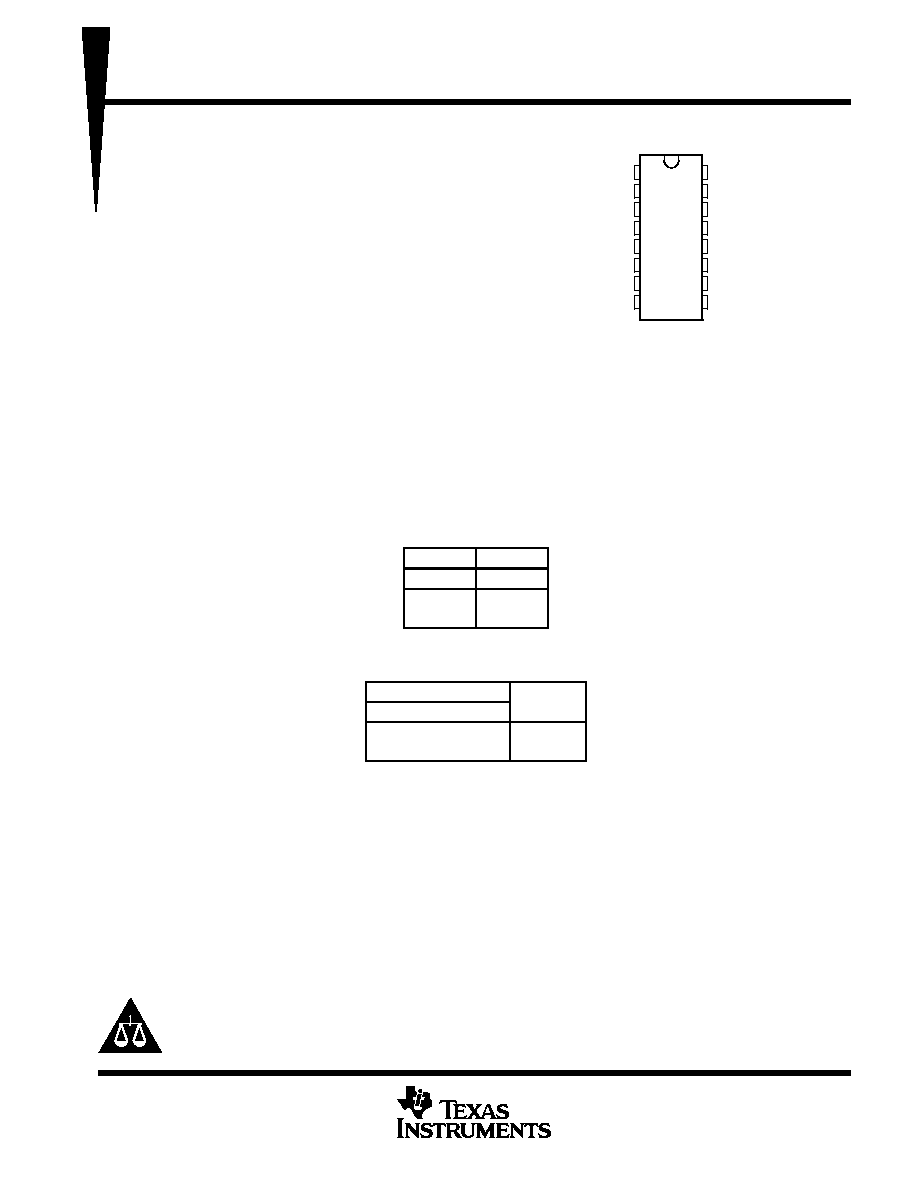
D OR N PACKAGE
(TOP VIEW)
AM26S10C
QUADRUPLE BUS TRANSCEIVERS
SLLS116C ≠ JANUARY 1977 ≠ REVISED MARCH 1997
2
POST OFFICE BOX 655303
∑
DALLAS, TEXAS 75265
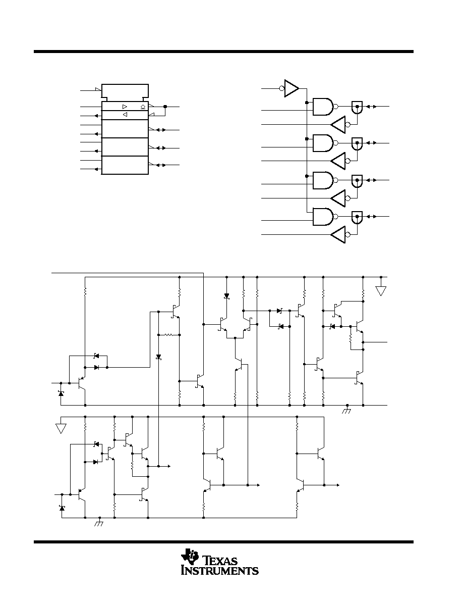
logic symbol
4R
3R
2R
1R
14
10
6
3
1
EN1
4B
15
3B
9
2B
7
1B
2
13
4D
11
3D
5
2D
4
1D
S
12
AM26S10C
These symbols are in accordance with ANSI/IEEE Std 91-1984
and IEC Publication 617-12.
12
S
1D
4
3
1R
2D
5
6
2R
3D
11
10
3R
4D
13
14
4R
15
4B
9
3B
7
2B
2
1B
AM26S10C
logic diagram (positive logic)
schematic (each transceiver)
V
V
B
D
VCC
R
GND
110
NOM
2 k
NOM
S
2.7 k
NOM
To Three
Other
Drivers
To One
Other
Receiver
To Two
Other
Receivers
AM26S10C
QUADRUPLE BUS TRANSCEIVERS
SLLS116C ≠ JANUARY 1977 ≠ REVISED MARCH 1997
3
POST OFFICE BOX 655303
∑
DALLAS, TEXAS 75265
absolute maximum ratings over operating free-air temperature range (unless otherwise noted)
Supply voltage, V
CC
(see Note 1)
≠ 0.5 V to 7 V
. . . . . . . . . . . . . . . . . . . . . . . . . . . . . . . . . . . . . . . . . . . . . . . . . . . .
Driver or strobe input voltage range, V
I
≠ 0.5 V to 5.5 V
. . . . . . . . . . . . . . . . . . . . . . . . . . . . . . . . . . . . . . . . . . . . .
Bus voltage range, driver output off, V
O
≠ 0.5 V to 5.25 V
. . . . . . . . . . . . . . . . . . . . . . . . . . . . . . . . . . . . . . . . . . . .
Driver or strobe input current range, I
I
≠ 30 mA to 5 mA
. . . . . . . . . . . . . . . . . . . . . . . . . . . . . . . . . . . . . . . . . . . . .
Driver output current, I
O
200 mA
. . . . . . . . . . . . . . . . . . . . . . . . . . . . . . . . . . . . . . . . . . . . . . . . . . . . . . . . . . . . . . . . .
Receiver output current, I
O
30 mA
. . . . . . . . . . . . . . . . . . . . . . . . . . . . . . . . . . . . . . . . . . . . . . . . . . . . . . . . . . . . . . . .
Continuous total power dissipation
See Dissipation Rating Table
. . . . . . . . . . . . . . . . . . . . . . . . . . . . . . . . . . . . .
Operating free-air temperature range, T
A
0
∞
C to 70
∞
C
. . . . . . . . . . . . . . . . . . . . . . . . . . . . . . . . . . . . . . . . . . . . . .
Storage temperature range, T
stg
≠ 65
∞
C to 150
∞
C
. . . . . . . . . . . . . . . . . . . . . . . . . . . . . . . . . . . . . . . . . . . . . . . . . . .
Lead temperature 1,6 mm (1/16 inch) from case for 10 seconds
260
∞
C
. . . . . . . . . . . . . . . . . . . . . . . . . . . . . . .
Stresses beyond those listed under "absolute maximum ratings" may cause permanent damage to the device. These are stress ratings only, and
functional operation of the device at these or any other conditions beyond those indicated under "recommended operating conditions" is not
implied. Exposure to absolute-maximum-rated conditions for extended periods may affect device reliability.
NOTE 1: All voltage values are with respect to network ground terminals connected together.
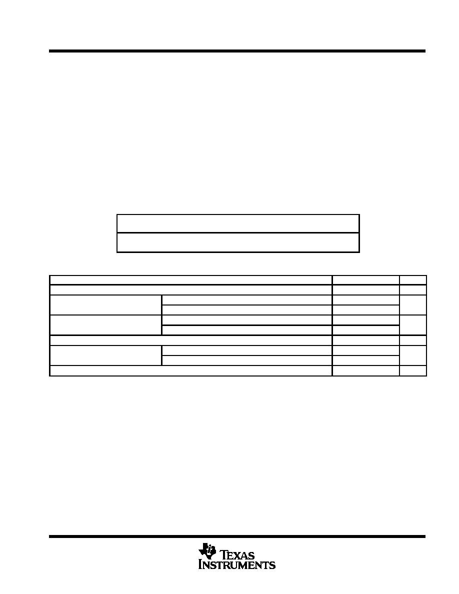
DISSIPATION RATING TABLE
PACKAGE
TA
25
∞
C
POWER RATING
DERATING FACTOR
ABOVE TA = 25
∞
C
TA = 70
∞
C
POWER RATING
D
950 mW
7.6 mW/
∞
C
608 mW
N
1150 mW
9.2 mW/
∞
C
736 mW
recommended operating conditions
MIN
NOM
MAX
UNIT
Supply voltage, VCC
4.75
5
5.25
V
High levael input voltage VIH
D or S
2
V
High-levael input voltage, VIH
B
2.25
V
Low level input voltage VIL
D or S
0.8
V
Low-level input voltage, VIL
B
1.75
V
Receiver high-level output current, IOH
≠ 1
mA
Low level output current IOL
Driver
100
mA
Low-level output current, IOL
Receiver
20
mA
Operating free-air temperature, TA
0
70
∞
C
AM26S10C
QUADRUPLE BUS TRANSCEIVERS
SLLS116C ≠ JANUARY 1977 ≠ REVISED MARCH 1997
4
POST OFFICE BOX 655303
∑
DALLAS, TEXAS 75265
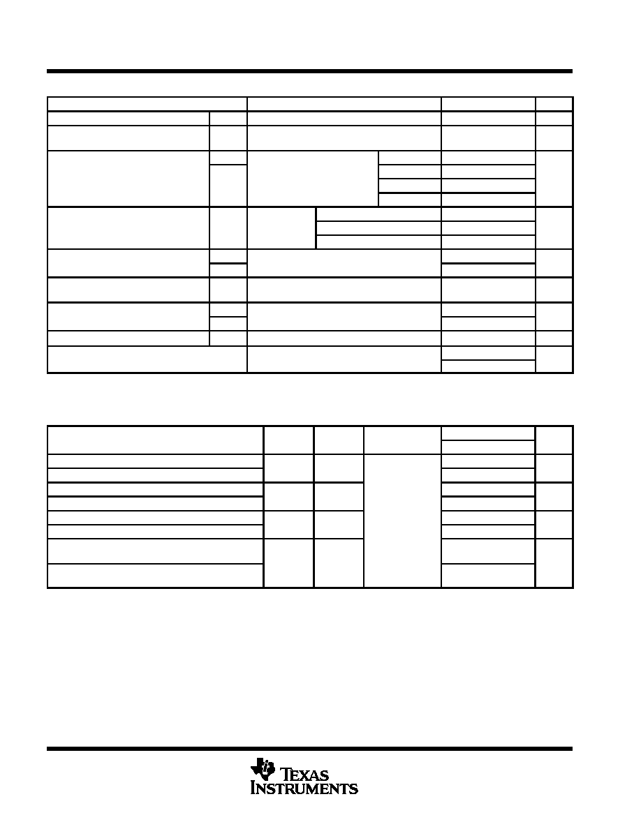
electrical characteristics over recommended operating free-air temperature range
PARAMETER
TEST CONDITIONS
MIN
TYP
MAX
UNIT
VIK
Input clamp voltage
D or S
VCC = 4.75 V,
II = ≠ 18 mA
≠ 1.2
V
VOH
High-level output voltage
R
VCC = 4.75 V,
IOH = ≠ 1 mA
VIH = 2 V,
VIL = 0.8 V,
2.7
3.4
V
R
IOL = 20 mA
0.5
VOH
Low level output voltage
VCC = 4.75 V,
VIH = 2 V,
IOL = 40 mA
0.33
0.5
V
VOH
Low-level output voltage
B
CC
,
VIL = 0.8 V
IH
,
IOL = 70 mA
0.42
0.7
V
IOL = 100 mA
0.51
0.8
V
2 V
VCC = 5.25 V, VO = 0.8 V
≠ 50
IO(off)
Off-stage output current
B
VIH = 2 V,
VIL = 0 8 V
VCC = 5.25 V, VO = 4.5 V
100
µ
A
(
)
VIL = 0.8 V
VCC = 0,
VO = 4.5 V
100
IIH
High level input current
D
VCC = 5 25 V
VI = 2 7 V
30
µ
A
IIH
High-level input current
S
VCC = 5.25 V,
VI = 2.7 V
20
µ
A
II
Input current at maximum
input voltage
D or S
VCC = 5.25 V,
VI = 5.5 V
100
µ
A
IIL
Low level input current
D
VCC = 5 25 V
VI = 0 4 V
≠ 0.54
mA
IIL
Low-level input current
S
VCC = 5.25 V,
VI = 0.4 V
≠ 0.36
mA
IOS
Short-circuit output current
R
VCC = 5.25 V
≠ 18
≠ 60
mA
ICC
Supply current
VCC = 5.25 V,
Strobe at 0 V,
No load,
45
70
mA
ICC
Supply current
CC
,
,
,
All driver outputs low
80
mA
All typical values are at TA = 25
∞
C and VCC = 5 V.
Not more than one output should be shorted to ground at a time, and duration of the short circuit should not exceed one second.
switching characteristics, V
CC
= 5 V, T
A
= 25
∞
C
PARAMETER
FROM
TO
TEST
AM26S10C
UNIT
PARAMETER
(INPUT)
(OUTPUT)
CONDITIONS
MIN
TYP
MAX
UNIT
tPLH Propagation delay time, low-to-high-level output
D
B
10
15
ns
tPHL Propagation delay time, high-to-low-level output
D
B
10
15
ns
tPLH Propagation delay time, low-to-high-level output
S
B
14
18
ns
tPHL Propagation delay time, high-to-low-level output
S
B
13
18
ns
tPLH Propagation delay time, low-to-high-level output
B
R
See Figure 1
10
15
ns
tPHL Propagation delay time, high-to-low-level output
B
R
See Figure 1
10
15
ns
tTLH
Transition time,
low-to-high-level output
B
4
10
ns
tTHL
Transition time,
high-to-low-level output
B
2
4
ns
AM26S10C
QUADRUPLE BUS TRANSCEIVERS
SLLS116C ≠ JANUARY 1977 ≠ REVISED MARCH 1997
5
POST OFFICE BOX 655303
∑
DALLAS, TEXAS 75265
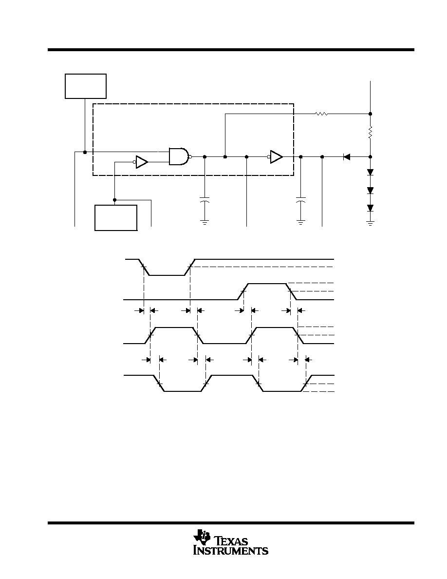
PARAMETER MEASUREMENT INFORMATION
Pulse
Generator
(see Note A)
D
S
Driver
15 pF
(see Note B)
Receiver
See Note C
50
280
VCC
B
R
TEST CIRCUIT
50 pF
(see Note B)
Pulse
Generator
(see Note A)
tPLH
B to R
tPHL
B to R
tPLH
B to R
tPHL
B to R
S to B
tPHL
tPLH
S to B
tPHL
D to B
tPLH
D to B
3 V
1.5 V
3 V
1.5 V
0 V
VOH
1.5 V
VOL
VOH
1.5 V
VOL
Driver Input
Strobe Input
Bus
Receiver Output
VOLTAGE WAVEFORMS
NOTES: A. The pulse generators have the following characteristics: ZO = 50
, tr = 10
±
5 ns.
B. Includes probe and jig capacitance.
C. All diodes are 1N916 or equivalent.
Figure 1. Test Circuit and Voltage Waveforms