 | ÐлекÑÑоннÑй компоненÑ: AMC7823 | СкаÑаÑÑ:  PDF PDF  ZIP ZIP |
Äîêóìåíòàöèÿ è îïèñàíèÿ www.docs.chipfind.ru
Burr Brown Products
from Texas Instruments
FEATURES
APPLICATIONS
DESCRIPTION
Out-of-Range
Alarm
Range
Threshold
ADC
Analog Input Signal Ground
TEMP
CH8
Ext. Ref _ IN
Current_Setting Resistor
Precision_Current
ADC Trigger
(External / Internal)
Channel Select
DAC-7
DAC-0
Sync. Load
(Ext./Internal)
Reference
DAC 7_OUT
DAC 0_OUT
CH0
CH1
CH2
CH3
CH4
CH5
CH6
CH7
On-Chip
Temperature
Sensor
Serial-Parallel Shift Reg
SPI Interface
CONVERT
ELDAC
SCLK
S
S
MOSI
MISO
GPIO
-0 /
ALR
0
GPIO
-3 /
ALR
3
GPIO
-4
GPIO
-5
A
V
DD
AGND
DV
DD
DGND
B
V
DD
(Ext. ADC
T
rigger)
(Ext. DAC
Sync Load)
Registers and
Control Logic
RESET
DA
V
GALR
AMC7823
SLAS453A APRIL 2005 REVISED OCTOBER 2005
ANALOG MONITORING AND CONTROL CIRCUIT
·
Communications Equipment
·
12-Bit ADC (200 kSPS)
·
Optical Networks
Eight Analog Inputs
·
Automatic Test Equipment
Input Range 0 to 2
×
V
REF
·
Industrial Control and Monitor
·
Programmable V
REF
, 1.25 V or 2.5 V
·
Medical Equipment
·
Eight 12-Bit DACs (2-
µ
s Settling Time)
·
Four Analog Input Out-of-Range Alarms
·
Six General-Purpose Digital I/O
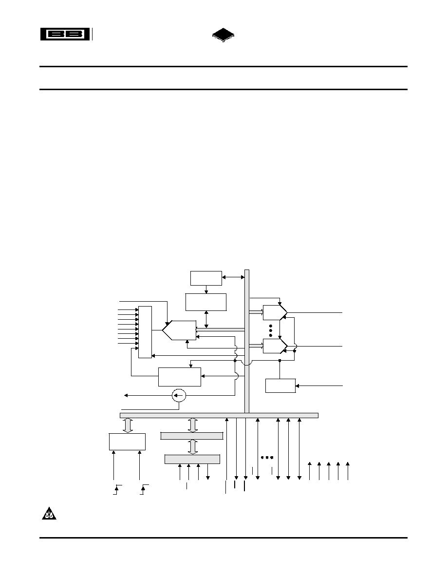
The AMC7823 is a complete analog monitoring and
·
Internal Bandgap Reference
control circuit that includes an 8-channel, 12-bit
·
On-Chip Temperature Sensor
analog-to-digital converter (ADC), eight 12-bit digital-
to-analog
converters
(DACs),
four
analog
input
·
Precision Current Source
out-of-range alarms, and six GPIOs to monitor analog
·
SPITM Interface, 3-V or 5-V Logic Compatible
signals and control external devices. Also, the
·
Single 3-V to 5-V Supply
AMC7823 has an internal sensor to monitor chip
temperature, and a precision current source to drive
·
Power-Down Mode/Low Power
remote thermistors, or RTDs, to monitor remote
·
Small Package (QFN-40, 6 × 6 mm)
temperatures.
Please be aware that an important notice concerning availability, standard warranty, and use in critical applications of Texas
Instruments semiconductor products and disclaimers thereto appears at the end of this data sheet.
SPI is a trademark of Motorola, Inc.
All trademarks are the property of their respective owners.
PRODUCTION DATA information is current as of publication date.
Copyright © 2005, Texas Instruments Incorporated
Products conform to specifications per the terms of the Texas
Instruments standard warranty. Production processing does not
necessarily include testing of all parameters.
www.ti.com
DESCRIPTION (CONTINUED)
ABSOLUTE MAXIMUM RATINGS
AMC7823
SLAS453A APRIL 2005 REVISED OCTOBER 2005
The AMC7823 has an internal programmable reference (+2.5 V or +1.25 V), and an SPI serial interface. An
external reference can be used as well. Typical power dissipation is 100 mW. The analog input range is 0 V to
+5 V, and the analog output range is 0 V to +2.5 V or 0 V to +5 V. The AMC7823 is ideal for multichannel
applications where low power and small size are critical. The AMC7823 is available in a 40-lead QFN package
and is fully specified over the 40°C to +85°C temperature range.
This integrated circuit can be damaged by ESD. Texas Instruments recommends that all integrated
circuits be handled with appropriate precautions. Failure to observe proper handling and installation
procedures can cause damage.
ESD damage can range from subtle performance degradation to complete device failure. Precision
integrated circuits may be more susceptible to damage because very small parametric changes could
cause the device not to meet its published specifications.
PACKAGE/ORDERING INFORMATION
(1)
PACKAGE-
SPECIFIED
LEAD
TEMPERATURE
PACKAGE
ORDERING
TRANSPORT
PRODUCT
(DESIGNATOR)
RANGE
MARKING
NUMBER
MEDIA, QUANTITY
AMC7823
AMC7823IRTAT
Tape and Reel, 250
AMC7823
QFN-40 (RTA)
40°C to 85°C
AMC7823
AMC7823IRTAR
Tape and Reel, 2000
(1)
For the most current package and ordering information, see the Package Option Addendum at the end of this document, or see the TI
web site at
www.ti.com
.
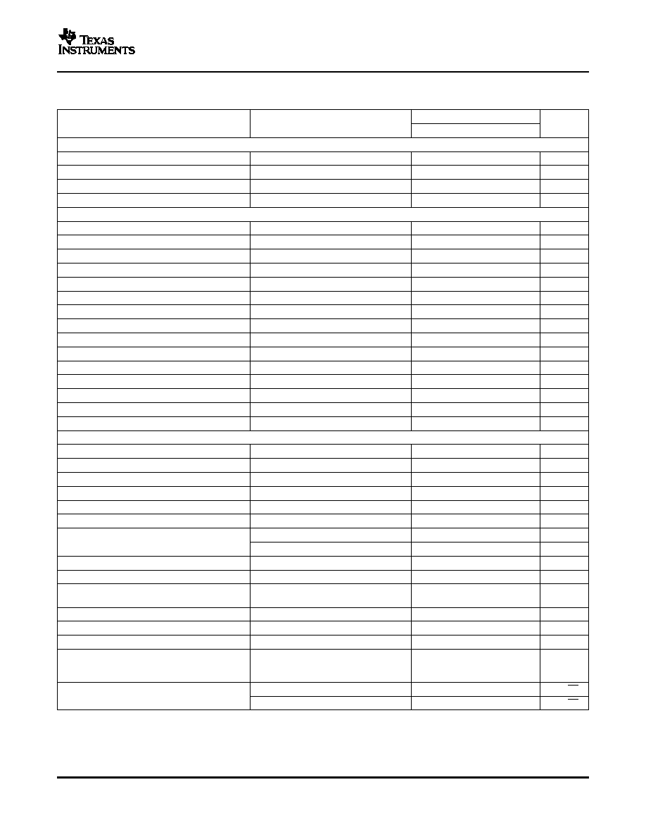
Over operating free-air temperature range unless otherwise noted(
(1)
)
AMC7823
UNIT
AV
DD
, DV
DD
, BV
DD
to GND
0.3 to +6
V
Digital input voltage to GND
0.3 to BV
DD
+ 0.3
V
Analog input voltage to GND
0.3 to AV
DD
+ 0.3
V
Input current, continuous
±20
mA
Input current, momentary
±100
mA
Operating temperature range
40 to +105
°C
Storage temperature range
65 to +150
°C
Junction temperature range (T
J
max)
+150
°C
Power dissipation
(T
J
max T
A
) /
JA
W
Thermal impedance,
JC
15
°C/W
Thermal impedance,
JA
60
°C/W
Lead temperature (soldering)
Vapor phase (60s)
+215
°C
Lead temperature (soldering)
Infrared (15s)
+220
°C
(1)
Stresses above those listed under absolute maximum ratings may cause permanent damage to the device. Exposure to absolute
maximum conditions for extended periods may affect device reliability.
2
www.ti.com
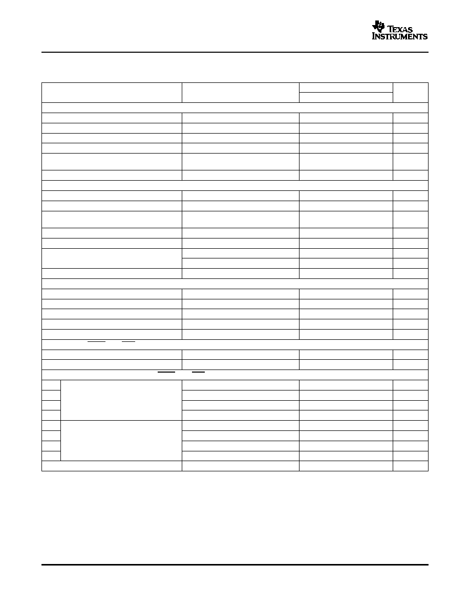
ELECTRICAL CHARACTERISTICS: +5 V
AMC7823
SLAS453A APRIL 2005 REVISED OCTOBER 2005
At 40°C to +85°C, AV
DD
= 5 V, DV
DD
= 5 V, BV
DD
= 3 V to 5 V, using external 2.5-V reference (unless otherwise noted).
AMC7823
PARAMETER
CONDITIONS
MIN
TYP
MAX
UNITS
ADC ANALOG INPUTS
Input voltage range
0
2 × V
REF
V
Input impedance
5
M
Input capacitance
15
pF
Input leakage current
±1
µA
ANALOG-TO-DIGITAL CONVERTER
Resolution
12
Bits
No missing codes
12
Bits
Integral linearity
±1
LSB
(1)
Differential linearity
±1
LSB
Offset error
±2
LSB
Offset error drift
±4
ppmFS/°C
Offset error match
0.5
1
LSB
Gain error
±6
LSB
Gain error match
0.3
1
LSB
Noise
70
µV
RMS
Power-supply rejection
AV
DD
= 5 V ±5%
70
dB
Throughput rate
200
kHz
Total conversion time
Scan Channels 0 through 7
45
µ
s
Total conversion time including temperature
Scan Channels 0 through 8
56
µ
s
Channel-to-channel isolation
V
IN
= 5 V
PP
at 10 kHz
0.5
LSB
DIGITAL-TO-ANALOG CONVERTER
(2)
Output voltage range
Programmable
0
2 × V
REF
V
Output current
Refer to
Typical Characteristics
±1
mA
Resolution
12
Bits
Integral linearity
(3)
±2
±8
LSB
Monotonicity
12
Bits
Differential linearity
±0.2
±1
LSB
Output range = 0 to V
REF
±0.5
±5
mV
Offset error
Output range = 0 to 2 x V
REF
±1
±10
mV
Offset error drift
±4
ppmFS/°C
Gain error
Output range = 0 to 2 x V
REF
±0.3
±1.0
%FS
Step between code 0x400 to 0xC00,
Settling time
2
µ
s
to ±1 LSB
Code change glitch
1 LSB change, in worst case
20
nV-s
Overshoot
Step between code 0x400 to 0xC00
200
mV
Crosstalk
Step between code 0x400 to 0xC00
< 0.5
LSB
Sine wave (1 kHz, 5 V
PP
) generated by
Signal-to-noise ratio
DAC, sampling at 400 kSPS,
74
dB
R
L
= 10 k
, C
L
= 100 pF.
Output buffer gain = 2
60
nV/
Hz
Output noise voltage density
Output buffer gain = 1
30
nV/
Hz
(1)
LSB means least significant bit.
(2)
DAC is tested with load of 25 k
in parallel with 100 pF to ground.
(3)
Measured from code 0x008 to 0xFFF.
3
www.ti.com
AMC7823
SLAS453A APRIL 2005 REVISED OCTOBER 2005
ELECTRICAL CHARACTERISTICS: +5 V (continued)
At 40°C to +85°C, AV
DD
= 5 V, DV
DD
= 5 V, BV
DD
= 3 V to 5 V, using external 2.5-V reference (unless otherwise noted).
AMC7823
PARAMETER
CONDITIONS
MIN
TYP
MAX
UNITS
PRECISION CURRENT SOURCE
Output current range
0.01
10
mA
Output current accuracy
I
out
= 100
µ
A
99.5
100.0
100.5
µ
A
Output current drift
I
out
= 100
µ
A
40
ppm/°C
Output impedance
I
out
= 100
µ
A
100
M
Compliance voltage of pin
3
4.25
V
I
out
= 10 mA
PRECISION_I_OUTPUT
Power-supply rejection ratio
60
dB
VOLTAGE REFERENCE (V
REF
)
Internal reference voltage
(4)
At 25°C
2.495
2.50
2.505
V
Internal reference drift
40°C to 85°C
±15
ppm/°C
Output impedance of pin EXT_REF_IN
10
k
as internal reference output
Short-circuit current
250
µ
A
External reference voltage
1.20
2.55
V
Internal reference selected
10
k
External reference input resistance
Internal reference de-selected
1
M
External reference input capacitance
5
pF
TEMPERATURE SENSOR
Temperature range
40
85
°C
Resolution
V
REF
= 2.5 V
3.2
°C
V
REF
= 1.25 V
1.6
°C
Accuracy
V
REF
= 2.5 V
±4
°C
V
REF
= 1.25 V
±
2.0
°C
LEVEL OF PIN GALR AND DAV
I
OH
= 0.7 mA
4
DV
DD
V
I
OL
= 180
µ
A
0
0.4
V
DIGITAL INPUT/OUTPUT, EXCEPT PIN GALR AND DAV
V
IH
BV
DD
= 5 V, I
IH
= 5
µ
A
3.5
BV
DD
+ 0.3
V
V
IL
BV
DD
= 5 V, I
IL
= 5
µ
A
0
0.8
V
Logic level
V
OH
BV
DD
= 5 V, I
OH
= 3 mA
4
BV
DD
V
V
OL
BV
DD
= 5 V,
OL
= 3 mA
0
0.4
V
V
IH
BV
DD
= 3 V, I
IH
= 5
µ
A
2.1
BV
DD
+ 0.3
V
V
IL
BV
DD
= 3 V, I
IL
= 5
µ
A
0
0.6
V
Logic level
V
OH
BV
DD
= 3 V, I
OH
= 3 mA
2.4
BV
DD
V
V
IL
BV
DD
= 3 V, I
OL
= 3 mA
0
0.4
V
Input capacitance
5
pF
(4)
Bit GREF in AMC Status/Configuration Register determines the internal reference voltage. The internal V
REF
= 2.5 V when GREF = 1,
and the internal V
REF
= 1.25 V when GREF = 0 (see
AMC Status/Configuration Register
for details).
4
www.ti.com
AMC7823
SLAS453A APRIL 2005 REVISED OCTOBER 2005
ELECTRICAL CHARACTERISTICS: +5 V (continued)
At 40°C to +85°C, AV
DD
= 5 V, DV
DD
= 5 V, BV
DD
= 3 V to 5 V, using external 2.5-V reference (unless otherwise noted).
AMC7823
PARAMETER
CONDITIONS
MIN
TYP
MAX
UNITS
POWER SUPPLY REQUIREMENTS
Power-supply voltage
AV
DD
Specified performance
2.7
5
5.5
V
DV
DD
(5)
Specified performance
2.7
5.5
V
BV
DD
(6)
Specified performance
2.7
5.5
V
In normal operation,
precision current source = 0, no DAC
15
20
Quiescent current of AV
DD
mA
load.
All power-down
1
Quiescent current of DV
DD
0.3
mA
Quiescent current of BV
DD
0.1
mA
Power dissipation
100
mW
TEMPERATURE RANGE
Specified performance
40
+85
°C
Storage
65
+150
°C
(5)
DV
DD
must equal AV
DD
.
(6)
BV
DD
must not be greater than AV
DD
or DV
DD
.
5
Document Outline