Lithium_Ion_Pack_Supervisor_for_3-_and_4-Cell_Packs
1
Features
Protects and individually moni-
tors three or four Li-Ion series
cells for overvoltage, undervolt-
age
Monitors pack for overcurrent
Designed for battery pack inte-
gration
Minimal external components
Drives external FET switches
Selectable overvoltage (V
OV
)
thresholds
-
Mask-programmable by
Unitrode
-
Standard version4.25V
Supply current: 25µA typical
Sleep current: 0.7µA typical
16-pin 150-mil narrow SOIC
General Description
The bq2058 Lithium Ion Pack Super-
visor is designed to control the charge
and discharge cell voltages for three or
four lithium ion (Li-Ion) series cells,
accommodating battery packs contain-
ing series/parallel configurations. The
low operating current does not over-
discharge the cells during periods of
storage and does not significantly in-
crease the system discharge load. The
bq2058 can be part of a low-cost Li-Ion
charge control system within the bat-
tery pack.
The bq2058 controls two external FETs
to limit the charge and discharge poten-
tials. The bq2058 allows charging when
each individual cell voltage is below V
OV
(overvoltage limit). If the voltage on any
cell exceeds V
OV
for a user-configurable
delay period (t
OVD
), the
CHG pin is
driven high, shutting off charge to the
battery pack. This safety feature pre-
vents overcharge of any cell within
the battery pack. After an overvolt-
age condition occurs, each cell must
fall below V
CE
(charge enable voltage)
for the bq2058 to re-enable charging.
The bq2058 protects batteries from
overdischarge. If the voltage on any
cell falls below V
UV
(undervoltage
limit) for a user-configurable delay pe-
riod (t
UVD
), the DSG output is driven
high, shutting off the battery dis-
charge. This safety feature prevents
overdischarge of any cell within the
battery pack.
The bq2058 also stops discharge on
detection of an overcurrent condition,
such as a short circuit. If an overcur-
rent condition occurs for a user-
configurable delay period (t
OCD
), the
DSG output is driven high, disconnect-
ing the load from the pack. DSG re-
mains high until removal of the short
circuit or overcurrent condition.
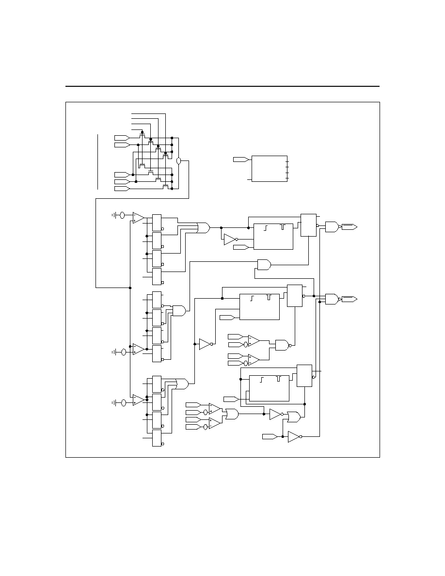
bq2058
Lithium Ion Pack Supervisor
for 3- and 4-Cell Packs
1
PN205801.eps
16-Pin Narrow SOIC
2
3
4
5
6
7
8
16
15
14
13
12
11
10
9
DSG
NSEL
UVD
OVD
OCD
VCC
CSH
BAT1P
CHG
CTL
VSS
CSL
BAT4N
BAT3N
BAT2N
BAT1N
Pin Connections
CHG
Charge control output
CTL
Pack disable input
V
SS
Low potential input
CSL
Current sense low-side
input
BAT
4N
Battery 4 negative input
BAT
3N
Battery 3 negative input
BAT
2N
Battery 2 negative input
BAT
1N
Battery 1 negative input
DSG
Discharge control output
NSEL
3- or 4-cell selection
UVD
Undervoltage delay input
OVD
Overvoltage delay input
OCD
Overcurrent delay input
V
CC
High potential input
CSH
Current sense high-side
input
BAT
1P
Battery 1 positive input
Pin Names
1/99 I
Pin Descriptions
CHG
Charge control output
This push-pull output controls the charge
path to the battery pack.
Charging is al-
lowed when low.
CTL
Pack disable input
When high, this input allows an external
source to disable the pack by making both
DSG and CHG inactive. For normal opera-
tion, the CTL pin is low.
V
SS
Low potential input
CSL
Overcurrent sense low-side input
This input is connected between the low-side
discharge FET (or sense resistor) and BAT
4N
to enable overcurrent sensing in the battery
pack's ground path.
BAT
4N
Battery 4 negative input
This input is connected to the negative termi-
nal of the cell designated BAT4 in Figure 2.
BAT
3N
Battery 3 negative input
This input is connected to the negative terminal
of the cell designated BAT3 in Figure 2.
BAT
2N
Battery 2 negative input
This input is connected to the negative termi-
nal of the cell designated BAT2 in Figure 2.
BAT
1N
Battery 1 negative input
This input is connected to the negative termi-
nal of the cell designated BAT1 in Figure 2.
This input is connected to BAT
1P
in a three-
cell configuration.
DSG
Discharge control output
This push-pull output controls the discharge
path to the battery pack. Discharge is al-
lowed when low.
NSEL
Number of cells input
This input selects the number of series cells
in the pack. NSEL should connect to V
CC
for
four cells and to V
SS
for three cells.
UVD
Undervoltage delay input
This input uses an external capacitor to V
CC
to set the undervoltage delay timing.
OVD
Overvoltage delay input
This input uses an external capacitor to V
CC
to set the overvoltage delay timing.
OCD
Overcurrent delay input
This input uses an external capacitor to V
CC
to set the overcurrent delay timing.
V
CC
High potential input
CSH
Overcurrent sense high-side input
T h i s i n p u t i s c o n n e c t e d b e t w e e n t h e
high-side discharge FET (or sense resistor)
and BAT
1P
to enable overcurrent sense in
the battery pack's positive supply path.
BAT
1P
Battery 1 positive input
This input is connected to the positive terminal
of the cell designated BAT1 in Figure 2.
2
bq2058
Number of Cells
Configuration Pins
Battery Pins
3 cells
BAT
1N
tied to BAT
1P
NSEL = V
SS
BAT
1N
Positive terminal of first cell
BAT
2N
Negative terminal of first cell
BAT
3N
Negative terminal of second cell
BAT
4N
Negative terminal of third cell
4 cells
NSEL = V
CC
BAT
1P
Positive terminal of first cell
BAT
1N
Negative terminal of first cell
BAT
2N
Negative terminal of second cell
BAT
3N
Negative terminal of third cell
BAT
4N
Negative terminal of fourth cell
Table 1. Pin Configuration for 3- and 4-Series Cells
3
bq2058
+
-
B1P
Sel1
Sel2
B1N
Sel3
Sel4
B4N
B2N
B3N
Pin 9
Pin 8
Pin 7
Pin 6
Pin 5
Sleep
Cell Inputs
NSEL
Clock
Sel4
Sel3
Sel2
Sel1
Sel3
Sel2
Sel1
Sel4
NSEL
Sleep
Pin 15
Number of Cells Select
Edge
Out
Non-Retrigger
Oneshot
Reset
Capacitor
D
CK
Reset
QB
Overcharge
OVD
Edge
Out
Non-Retrigger
Oneshot
Reset
Capacitor
D
CK
Reset
QB
Sleep
UVD
Edge
Out
Non-Retrigger
Oneshot
Reset
Capacitor
D
CK
Reset
QB
OCD
Any_Above_VOV
All_Below_VCE
Q
CTL
Pin 2
External Output Control
Pin 14
Charge Off Delay Capacitor Input
Sense High-side Input
Sense Low-side Input
70mV
+
+
+
+
70mV
Overcurrent Delay
Capacitor Input
Pin 12
Pin 5
Pin 4
Pin 9
Pin 10
Any_Below_VUV
Pin 13
Discharge Off Delay Capacitor Input
D
CK
QB
Q
D
CK
QB
Q
D
CK
QB
Q
D
CK
QB
Q
D
CK
QB
Q
D
CK
QB
Q
D
CK
QB
Q
D
CK
QB
Q
D
CK
QB
Q
D
CK
QB
Q
D
CK
QB
Q
D
CK
QB
Q
Sel4
Sel3
Sel2
Sel1
Sel4
Sel3
Sel2
Sel1
Sel4
Sel3
Sel2
Sel1
VUV
+
VCE
+
VOV
+
Charge Control
Output
Discharge Control
Output
Chip Negative
Supply
CHG
Overcurrent
Pin 3
Pin 1
Pin 16
CSH
B1P
B4N
CSL
Pin 5
Pin 4
Pin 9
Pin 10
CSH
B1P
B4N
CSL
DSG
160mV
160mV
Figure 1. Block Diagram
Functional Description
Figure 1 is a block diagram outlining the major compo-
nents of the bq2058. Figure 2 shows a 3- or 4-cell pack
supervisor circuit. The following sections detail the vari-
ous functional aspects of the bq2058.
Thresholds
The bq2058 monitors the lithium ion pack for the condi-
tions listed below. Shown with these conditions are the
respective thresholds used to determine if that condition
exists:
I
Overvoltage (V
OV
)
I
Undervoltage (V
UV
)
I
Overcurrent (V
OCH
, V
OCL
)
I
Charge Enable (V
CE
)
I
Charge Detect (V
CD
)
The bq2058 samples a cell every 40ms (typical). Every
sample is a fully differential measurement of each cell.
During this sample period, the bq2058 compares the
measurements with these thresholds to determine if any
of the these conditions exist: V
OV
, V
UV
, and V
CE
.
Overcurrent and charge detect are conditions that are
not sampled, but are continuously monitored.
Initialization
On initial power-up, such as connecting the battery pack
for the first time to the bq2058, the bq2058 enters the
low-power sleep mode, disabling the DSG output. It is
recommended that a top to bottom cell connection
be made at pack assembly for proper initializa-
tion. A charging supply must be applied to the bq2058
circuit to enable the pack. See Low-Power Sleep Mode
and Charge Detect sections.
4
bq2058
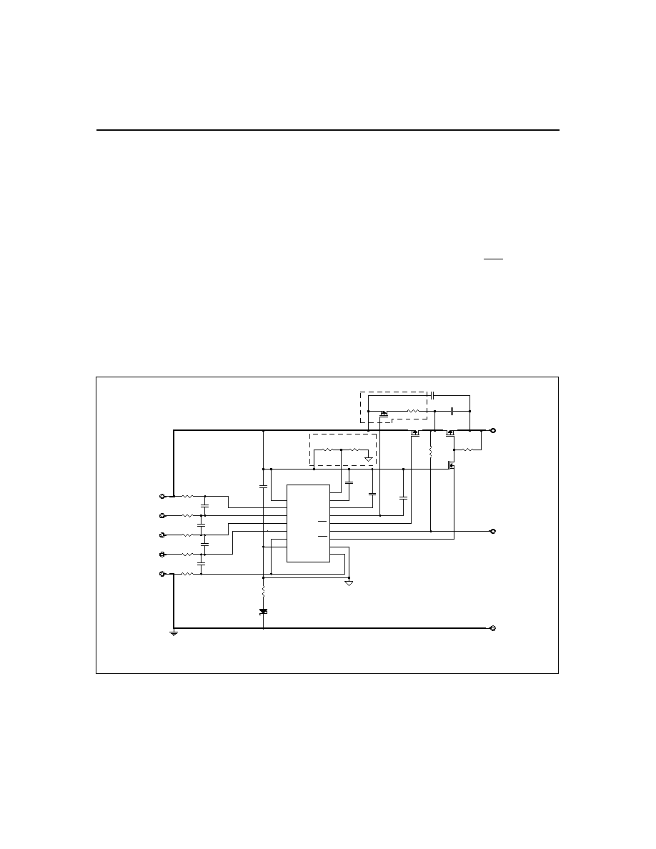
POS
Q1
Si4435DY
C6
0.1uF
C8
0.1uF
Q2
Si4435DY
Q4
ZVP3306F
R2
6.98K
* See note 1.
D1
BAT54
* See note 2.
Notes:
1. For automatic short circuit recovery.
B1P to B1N for 3-cells.
2. Remove R11 for 4-cell. Remove R10 and connect
B1P
R3
10K
C1
0.001uF
CSH
10
VCC
11
BAT1P
9
BAT1N
8
BAT2N
7
BAT3N
6
BAT4N
5
VSS
3
CSL
4
OVD
13
OCD
12
UVD
14
DSG
16
CHG
1
CTL
2
NSEL
15
U1
bq2058
R10
0 Ohm
4-Cell
C9
0.1uF
R11
0 Ohm
3-Cell
C7
0.01uF
C5
0.1uF
C10
0.1uF
R6
100K
R9
1M
Q3
2N7002
TP1
B1N
B2N
B3N
B4N
R4
10K
R5
10K
R7
10K
R8
10K
C2
0.001uF
C3
0.001uF
C4
0.001uF
R1
2.7K
NEG
Figure 2. 3- or 4-Cell Li-Ion Battery Pack Supervisor
Low-Power Sleep Mode
The bq2058 enters the low-power sleep mode in two dif-
ferent ways:
1.
On initial power-up.
2.
After the detection of an undervoltage condi-
tionV
UV
.
When the bq2058 enters the low-power sleep mode, DSG
is driven high and the device consumes 0.7
µA (typical).
The bq2058 only comes out of low-power sleep mode
when a valid charge-detect condition exists.
Charge Detect
The bq2058 continuously monitors for a charge-detect con-
dition. A valid charge-detect condition exists when either
of the conditions are true:
CSL < BAT
4N
- 70mV (V
CD
)
CSH > BAT
1P
+ 70mV (V
CD
)
A valid charge-detect enables the DSG output, allowing
charging of the lithium ion cells. This is accomplished
by applying the charging supply to the pack.
Undervoltage
Undervoltage (or overdischarge) protection is asserted
when any cell voltage drops below the V
UV
threshold
and remains below the V
UV
threshold for a time
exceeding a user-configurable delay (t
UVD
).
The DSG
output
is driven high disabling the discharge of the
pack.
The bq2058 then enters the low-power sleep
mode.
Overvoltage
Overvoltage (or overcharge) protection is asserted when
any cell voltage exceeds the V
OV
threshold and remains
above the V
OV
threshold for a time exceeding a user-
configurable delay (t
OVD
). The CHG pin is driven high,
disabling charge into the battery pack. Charging is dis-
abled until a valid charge enable exists. See Charge En-
able section.
Important note: If any battery pin floats (BAT
1P
,
BAT
1N
4N
), the bq2058 assumes an overvoltage has
occurred.
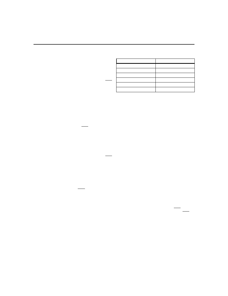
Because of different manufacturers specifications for
overvoltage thresholds, the bq2058 can be available with
different V
OV
options. Table 2 summarizes these differ-
ent voltage thresholds.
The overvoltage threshold limits are programmed
at Unitrode.
The bq2058 is the standard option
that is more readily available for sampling and
prototyping purposes.
Please contact Unitrode
for other voltage threshold and tolerance options.
Charge Enable
A valid charge enable indicates that an overvoltage
(overcharge) condition no longer exists and that the
pack is ready to accept further charge. Once overvoltage
protection is asserted, charging will not be enabled un-
til all cell voltages fall below V
CE
. The V
CE
threshold is
a function of V
OV,
and changes with different V
OV
lim-
its.
V
CE
= V
OV
- 150mV
Overcurrent
The bq2058 detects an overcurrent (or short circuit) con-
dition only in the discharge direction. Overcurrent pro-
tection is asserted when either of the conditions occurs
and remain for a time exceeding a user-configurable de-
lay (t
OCD
):
CSL > BAT
4N
+ V
OCL
CSH < BAT
1P
- V
OCH
where:
V
OCL
= 160mV (low-side detect)
V
OCH
= 160mV (high-side detect)
When either of these conditions occurs, DSG is driven
high, disconnecting the load from the pack.
DSG re-
mains high until both of the voltage conditions are false,
indicating removal of the short-circuit condition.
The
user can facilitate clearing these conditions by inserting
the battery pack into a charger.
The low-side overcurrent sense can be disabled by con-
necting CSL to BAT
4N
. This ensures that CSL is never
greater than BAT
4N
. If low-side detection is disabled,
high-side detection must be used with CSH.
5
bq2058
Part No.
V
OV
Limit
bq2058
4.25V
bq2058C
4.325
bq2058D
4.30V
bq2058G*
4.375V
bq2058R
4.35V
bq2058W
3.4V
Table 2. Overvoltage Threshold Options