 | –≠–ª–µ–∫—Ç—Ä–æ–Ω–Ω—ã–π –∫–æ–º–ø–æ–Ω–µ–Ω—Ç: BQ2004 | –°–∫–∞—á–∞—Ç—å:  PDF PDF  ZIP ZIP |
Features
Fast charge and conditioning of
nickel cadmium or nickel-metal
hydride batteries
Hysteretic PWM switch-mode
current regulation or gated con-
trol of an external regulator
Easily integrated into systems or
used as a stand-alone charger
Pre-charge qualification of tem-
perature and voltage
Configurable, direct LED outputs
display battery and charge status
Fast-charge termination by tem-
perature/
time, peak volume de-
tection, -
V, maximum voltage,
maximum temperature, and maxi-
mum time
Optional top-off charge and
pu ls e d cu rre nt mai nten anc e
charging
Logic-level controlled low-power
mode (< 5
µA standby current)
General Description
The bq2004 Fast Charge IC provides
comprehensive fast charge control
functions together with high-speed
switching power control circuitry on a
monolithic CMOS device.
Integration of closed-loop current
control circuitry allows the bq2004
to be the basis of a cost-effective so-
lution for stand-alone and system-
integrated chargers for batteries of
one or more cells.
Switch-activated discharge-before-
charge allows bq2004-based chargers
to support battery conditioning and
capacity determination.
High-efficiency power conversion is
accomplished using the bq2004 as a
hysteretic PWM controller for
switch-mode regulation of the charg-
ing current. The bq2004 may alterna-
tively be used to gate an externally
regulated charging current.
Fast charge may begin on application
of the charging supply, replacement
of the battery, or switch depression.
For safety, fast charge is inhibited
unless/until the battery tempera-
ture and voltage are within config-
ured limits.
Temperature, voltage, and time are
monitored throughout fast charge.
Fast charge is terminated by any of
the following:
n
Rate of temperature time
(
T/t)
n
Peak voltage detection (PVD)
n
Negative delta voltage (-
V)
n
Maximum voltage
n
Maximum temperature
n
Maximum time
After fast charge, optional top-off
and pulsed current maintenance
phases are available.
1
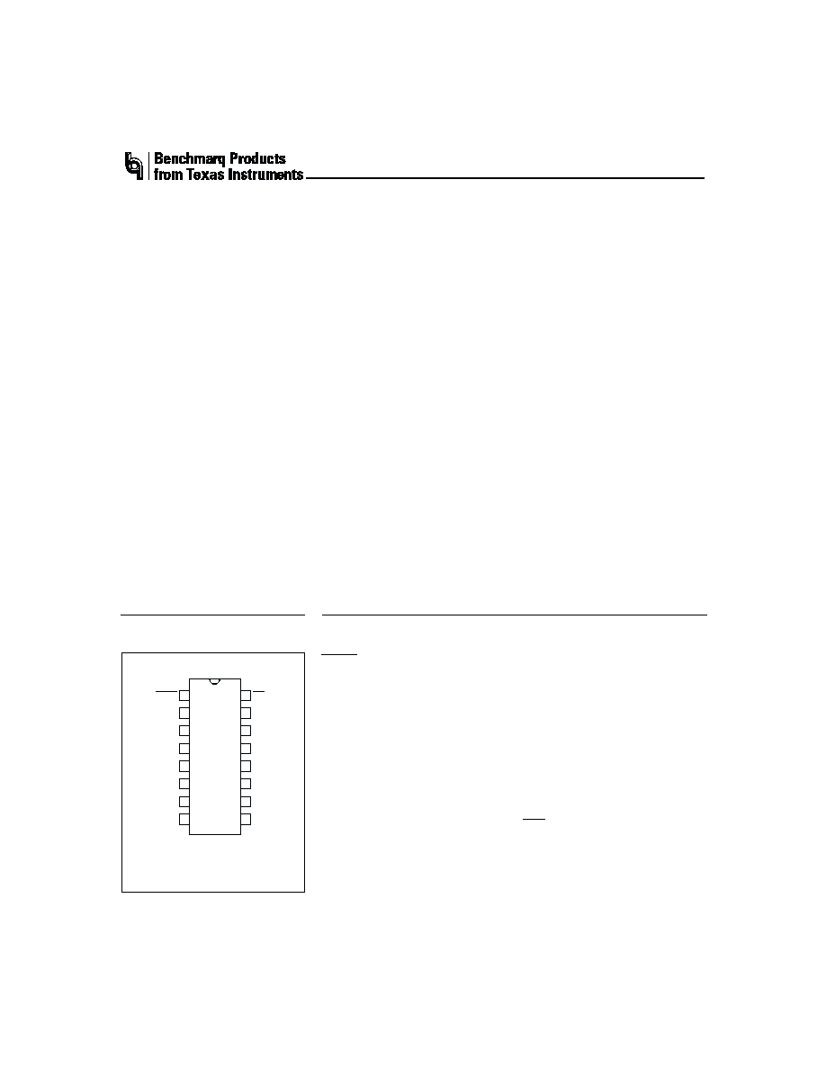
Fast-Charge IC
bq2004
DCMD
Discharge command
DSEL
Display select
VSEL
Voltage termination
select
TM
1
Timer mode select 1
TM
2
Timer mode select 2
TCO
Temperature cutoff
TS
Temperature sense
BAT
Battery voltage
1
PN2004E01.eps
16-Pin Narrow DIP
or Narrow SOIC
2
3
4
5
6
7
8
16
15
14
13
12
11
10
9
INH
DIS
MOD
VCC
VSS
LED2
LED1
SNS
DCMD
DSEL
VSEL
TM1
TM2
TCO
TS
BAT
SNS
Sense resistor input
LED
1
Charge status output 1
LED
2
Charge status output 2
V
SS
System ground
V
CC
5.0V
±10% power
MOD
Charge current control
DIS
Discharge control
output
INH
Charge inhibit input
Pin Connections
SLUS063≠JUNE 1999 F
Pin Names

Pin Descriptions
DCMD
Discharge-before-charge control input
The DCMD input controls the conditions
that enable discharge-before-charge. DCMD
is pulled up internally.
A negative-going
pulse on DCMD initiates a discharge to end-
of-discharge voltage (EDV) on the BAT pin,
followed by a new charge cycle start. Tying
D C M D t o g r o u n d e n a b l e s a u t o m a t i c
discharge-before-charge on every new charge
cycle start.
DSEL
Display select input
This three-state input configures the charge
status display mode of the LED
1
and LED
2
outputs. See Table 2.
VSEL
Voltage termination select input
This three-state input controls the voltage-
termination technique used by the bq2004.
When high, PVD is active.
When floating,
-
V is used. When pulled low, both PVD and
-
V are disabled.
TM
1
≠
TM
2
Timer mode inputs
TM
1
and TM
2
are three-state inputs that
configure the fast charge safety timer, voltage
termination hold-off time, "top-off ", and
trickle charge control. See Table 1.
TCO
Temperature cut-off threshold input
Input to set maximum allowable battery
temperature.
If the potential between TS
and SNS is less than the voltage at the TCO
input, then fast charge or top-off charge is ter-
minated.
TS
Temperature sense input
Input, referenced to SNS,
for an external
thermister monitoring battery temperature.
BAT
Battery voltage input
BAT is the battery voltage sense input, refer-
enced to SNS.
This is created by a high-
impedance resistor-divider network con-
nected between the positive and the negative
terminals of the battery.
SNS
Charging current sense input
SNS controls the switching of MOD based on
an external sense resistor in the current
path of the battery. SNS is the reference po-
tential for both the TS and BAT pins.
If
SNS is connected to V
SS
, then MOD switches
high at the beginning of charge and low at
the end of charge.
LED
1
≠
LED
2
Charge status outputs
Push-pull outputs indicating charging
status. See Table 2.
V
SS
Ground
V
CC
V
CC
supply input
5.0V,
±10% power input.
MOD
Charge current control output
MOD is a push-pull output that is used to
control the charging current to the battery.
MOD switches high to enable charging cur-
rent to flow and low to inhibit charging
current flow.
DIS
Discharge control output
Push-pull output used to control an external
transistor to discharge the battery before
charging.
INH
Charge inhibit input
When low, the bq2004 suspends all charge
actions, drives all outputs to high imped-
ance, and assumes a low-power operational
state. When transitioning from low to high, a
new charge cycle is started.
2
bq2004
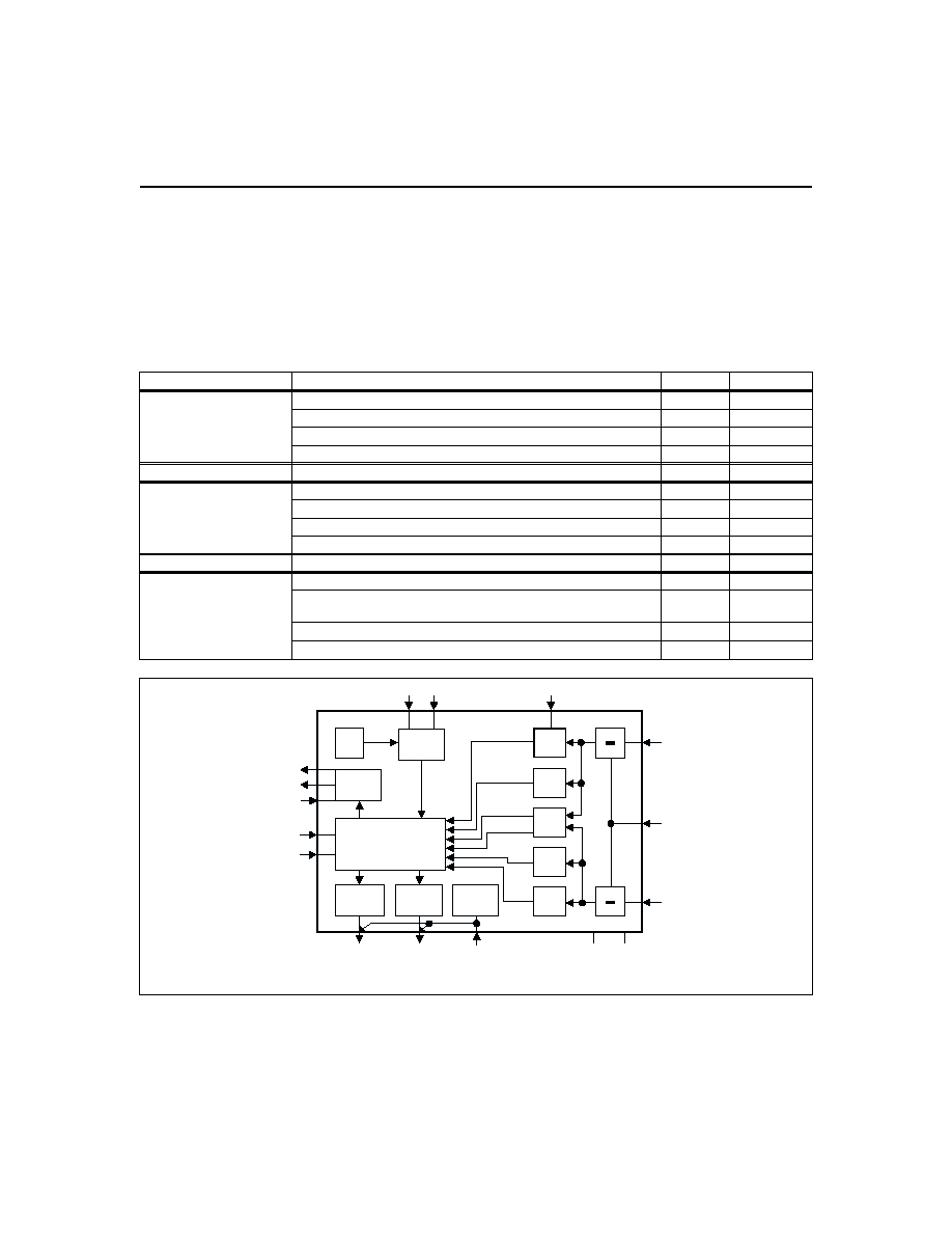
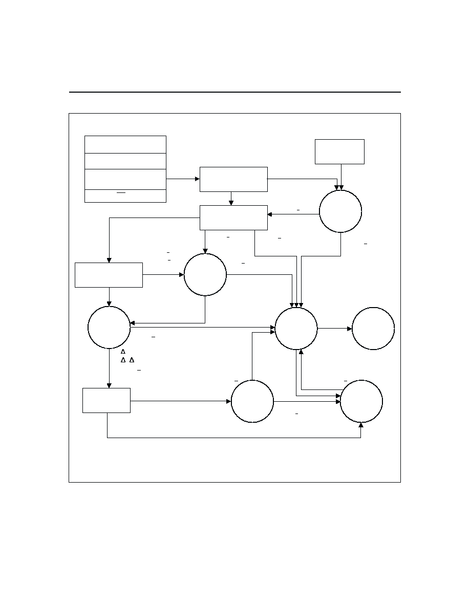
Functional Description
Figure 3 shows a block diagram and Figure 4 shows a
state diagram of the bq2004.
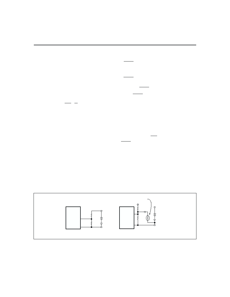
Battery Voltage and Temperature
Measurements
Battery voltage and temperature are monitored for
maximum allowable values. The voltage presented on
the battery sense input, BAT, should represent a
two-cell potential for the battery under charge.
A
resistor-divider ratio of:
RB1
RB2
=
N
2
- 1
is recommended to maintain the battery voltage within
the valid range, where N is the number of cells, RB1 is
the resistor connected to the positive battery terminal,
and RB2 is the resistor connected to the negative bat-
tery terminal. See Figure 1.
Note: This resistor-divider network input impedance to
end-to-end should be at least 200k
and less than 1M.
A ground-referenced negative temperature coefficient ther-
mistor placed in proximity to the battery may be used as a
low-cost temperature-to-voltage transducer. The tempera-
ture sense voltage input at TS is developed using a
resistor-thermistor network between V
CC
and V
SS
.
See
Figure 1. Both the BAT and TS inputs are referenced to
SNS, so the signals used inside the IC are:
V
BAT
- V
SNS
= V
CELL
and
V
TS
- V
SNS
= V
TEMP
Discharge-Before-Charge
The DCMD input is used to command discharge-before-
charge via the DIS output. Once activated, DIS becomes
active (high) until V
CELL
falls below V
EDV,
at which time
DIS goes low and a new fast charge cycle begins.
The DCMD input is internally pulled up to V
CC
(its inac-
tive state). Leaving the input unconnected, therefore,
results in disabling discharge-before-charge. A negative
going pulse on DCMD initiates discharge-before-charge
at any time regardless of the current state of the
bq2004. If DCMD is tied to V
SS
, discharge-before-charge
will be the first step in all newly started charge cycles.
Starting a Charge Cycle
A new charge cycle (see Figure 2) is started by:
1.
V
CC
rising above 4.5V
2.
V
CELL
falling through the maximum cell voltage,
V
MCV
where:
V
MCV
= 0.8
V
CC
± 30mV
3.
A transition on the INH input from low to high.
If DCMD is tied low, a discharge-before-charge is exe-
cuted as the first step of the new charge cycle. Other-
wise, pre-charge qualification testing is the first step.
The battery must be within the configured temperature
and voltage limits before fast charging begins.
The valid battery voltage range is V
EDV
< V
BAT
< V
MCV
where:
V
EDV
= 0.4
V
CC
± 30mV
The valid temperature range is V
HTF
< V
TEMP
< V
LTF
,
where:
3
bq2004
Fg2004a.eps
N
T
C
bq2004
VCC
PACK +
PACK -
TS
SNS
RT1
RT2
RB2
RB1
bq2004
Negative Temperature
Coefficient Thermister
PACK+
PACK-
BAT
SNS
Figure 1. Voltage and Temperature Monitoring
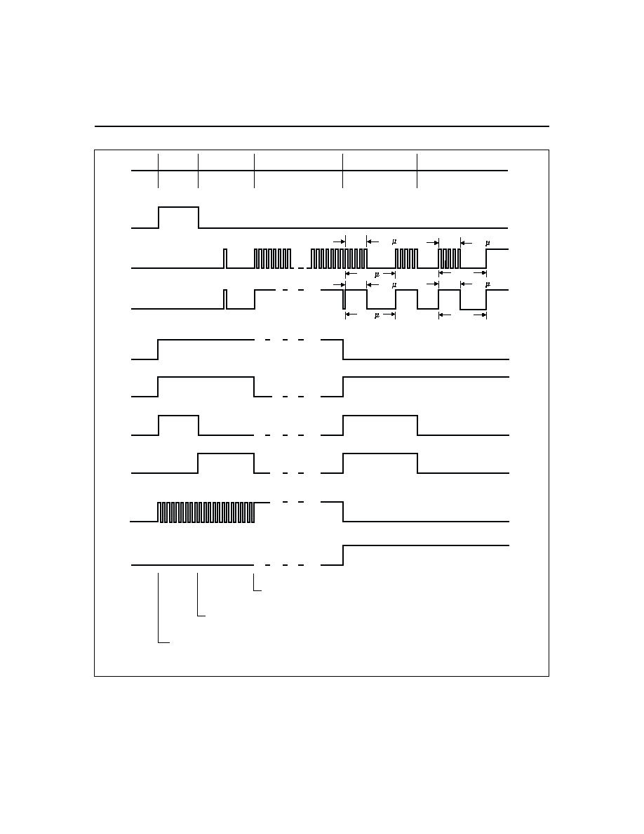
4
Fast Charging
Top-Off
(Optional)
TD200401a.eps
Dis-
charge
(Optional)
Charge
Pending*
(Pulse-Trickle)
DIS
MOD
MOD
Mode 1, LED2 Status Output
Discharge-Before-Charge started
or
Battery discharged to 0.4
*
VCC. Battery outside
temperature/voltage limits.
Battery within temperature/voltage limits.
Pulse-Trickle
Switch-mode
Configuration
External
Regulation
(
SNS Grounded)
Mode 1, LED1 Status Output
Mode 2, LED2 Status Output
Mode 2, LED1 Status Output
Mode 3, LED2 Status Output
Mode 3, LED1 Status Output
260 s
2080 s
260 s
2080 s
260 s
Note*
260 s
Note*
*See Table 3 for pulse-trickle period.
Figure 2. Charge Cycle Phases
bq2004
V
LTF
= 0.4
V
CC
± 30mV
V
HTF
= [(1/4
V
LTF
) + (3/4
V
TCO
)]
± 30mV
Note: The low temperature fault (LTF) threshold is not
enforced if
the IC is configured for PVD termination
(VSEL = high).
V
TCO
is the voltage presented at the TCO input pin, and is
configured by the user with a resistor divider between V
CC
and ground. The allowed range is 0.2 to 0.4
V
CC
.
If the temperature of the battery is out of range, or the
voltage is too low, the chip enters the charge pending
state and waits for both conditions to fall within their al-
lowed limits. The MOD output is modulated to provide
the configured trickle charge rate in the charge pending
state.
There is no time limit on the charge pending
state; the charger remains in this state as long as the
voltage or temperature conditons are outside of the al-
lowed limits. If the voltage is too high, the chip goes to
the battery absent state and waits until a new charge
cycle is started.
Fast charge continues until termination by one or more
of the six possible termination conditions:
n
Delta temperature/delta time (
T/t)
n
Peak voltage detection (PVD)
n
Negative delta voltage (-
V)
n
Maximum voltage
n
Maximum temperature
n
Maximum time
PVD and -
V Termination
The bq2004 samples the voltage at the BAT pin once
every 34s. When -
V termination is selected, if V
CELL
is
lower than any previously measured value by 12mV
±4mV (6mV/cell), fast charge is terminated. When PVD
termination is selected, if V
CELL
is lower than any previ-
ously measured value by 6mV
±2mV (3mV/cell), fast
charge is terminated. The PVD and -
V tests are valid
in the range 0.4
V
CC
< V
CELL
< 0.8
V
CC
.
Voltage Sampling
Each sample is an average of voltage measurements
taken 57
µs apart. The IC takes 32 measurements in
PVD mode and 16 measurements in -
V mode. The re-
sulting sample periods (9.17ms and 18.18ms, respec-
tively) filter out harmonics centered around 55Hz and
109Hz. This technique minimizes the effect of any AC
line ripple that may feed through the power supply from
either 50Hz or 60Hz AC sources. Tolerance on all tim-
ing is
±16%.
Voltage Termination Hold-off
A hold-off period occurs at the start of fast charging.
During the hold-off period, -
V termination is disabled.
This avoids premature termination on the voltage
spikes sometimes produced by older batteries when
fast-charge current is first applied.
T/t, maximum
voltage and maximum temperature terminations are
not affected by the hold-off period.
T/t Termination
The bq2004 samples at the voltage at the TS pin every
34s, and compares it to the value measured two samples
earlier. If V
TEMP
has fallen 16mV
±4mV or more, fast
charge is terminated. If VSEL = high, the
T/t termi-
nation test is valid only when V
TCO
< V
TEMP
< V
TCO
+
0.2
V
CC
. Otherwise the
T/t termination test is valid
only when V
TCO
< V
TEMP
< V
LTF
.
Temperature Sampling
Each sample is an average of 16 voltage measurements
taken 57
µs apart. The resulting sample period
(18.18ms) filters out harmonics around 55Hz. This tech-
nique minimizes the effect of any AC line ripple that
may feed through the power supply from either 50Hz or
60Hz AC sources. Tolerance on all timing is
±16%.
Maximum Voltage, Temperature, and Time
Anytime V
CELL
rises above V
MCV,
the LEDs go off and
charging ceases immediately. If V
CELL
then falls back be-
low V
MCV
before t
MCV
= 1.5s
±0.5s, the chip transitions to
the Charge Complete state (maximum voltage termina-
tion). If V
CELL
remains above V
MCV
at the expiration of
t
MCV,
the bq2004 transitions to the Battery Absent state
(battery removal). See Figure 4.
Maximum temperature termination occurs anytime
V
TEMP
falls below the temperature cutoff threshold
V
TCO
.
Unless PVD termination is enabled (VSEL =
high), charge will also be terminated if V
TEMP
rises
above the low temperature fault threshold, V
LTF
, after
fast charge begins. The V
LTF
threshold is not enforced
when the IC is configured for PVD termination.
Maximum charge time is configured using the TM pin.
Time settings are available for corresponding charge
rates of C/4, C/2, 1C, and 2C. Maximum time-out termi-
nation is enforced on the fast-charge phase, then reset,
and enforced again on the top-off phase, if selected.
There is no time limit on the trickle-charge phase.
5
bq2004
VSEL Input
Voltage Termination
Low
Disabled
Float
-
V
High
PVD
Top-off Charge
An optional top-off charge phase may be selected to
follow fast charge termination for the C/2 through 4C
rates. This phase may be necessary on NiMH or other
battery chemistries that have a tendency to terminate
charge prior to reaching full capacity. With top-off en-
abled, charging continues at a reduced rate after
fast-charge termination for a period of time equal to
the fast-charge safety time (See Table 1.) During top-
off, the MOD pin is enabled at a duty cycle of 260
µs ac-
tive for every 1820
µs inactive. This modulation results
in an average rate 1/8th that of the fast charge rate.
Maximum voltage, time, and temperature are the only
termination methods enabled during top-off.
Pulse-Trickle Charge
Pulse-trickle charging follows the fast charge and op-
tional top-off charge phases to compensate for self-
discharge of the battery while it is idle in the charger.
The configured pulse-trickle rate is also applied in the
charge pending state to raise the voltage of an over-
discharged battery up to the minimum required before
fast charge can begin.
In the pulse-trickle mode, MOD is active for 260
µs of a
period specified by the settings of TM1 and TM2. See
Table 1. The resulting trickle-charge rate is C/64 when
top-off is enabled and C/32 when top-off is disabled.
Both pulse trickle and top-off may be disabled by tying
TM1 and TM2 to V
SS
.
Charge Status Indication
Charge status is indicated by the LED
1
and LED
2
out-
puts. The state of these outputs in the various charge cy-
cle phases is given in Table 2 and illustrated in Figure 2.
In all cases, if V
CELL
exceeds the voltage at the MCV
pin, both LED
1
and LED
2
outputs are held low regard-
less of other conditions. Both can be used to directly
drive an LED.
Charge Current Control
The bq2004 controls charge current through the MOD
output pin. The current control circuitry is designed to
support implementation of a constant-current switching
regulator or to gate an externally regulated current
source.
When used in switch mode configuration, the nominal
regulated current is:
I
REG
= 0.225V/R
SNS
Charge current is monitored at the SNS input by the
voltage drop across a sense resistor, R
SNS
, between the
low side of the battery pack and ground. R
SNS
is sized to
provide the desired fast charge current.
If the voltage at the SNS pin is less than V
SNSLO
, the
MOD output is switched high to pass charge current to
the battery.
6
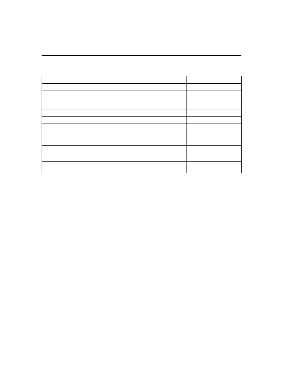
Corresponding
Fast-Charge
Rate
TM1
TM2
Typical
Fast-Charge Safety
Time (minutes)
Typical
PVD, -
V Hold-Off
Time (seconds)
Top-Off
Rate
Pulse-
Trickle
Rate
Pulse-
Trickle
Period (Hz)
C/4
Low
Low
360
137
Disabled
Disabled
Disabled
C/2
Float
Low
180
820
Disabled
C/32
240
1C
High
Low
90
410
Disabled
C/32
120
2C
Low
Float
45
200
Disabled
C/32
60
4C
Float
Float
23
100
Disabled
C/32
30
C/2
High
Float
180
820
C/16
C/64
120
1C
Low
High
90
410
C/8
C/64
60
2C
Float
High
45
200
C/4
C/64
30
4C
High
High
23
100
C/2
C/64
15
Note:
Typical conditions = 25∞C, V
CC
= 5.0V.
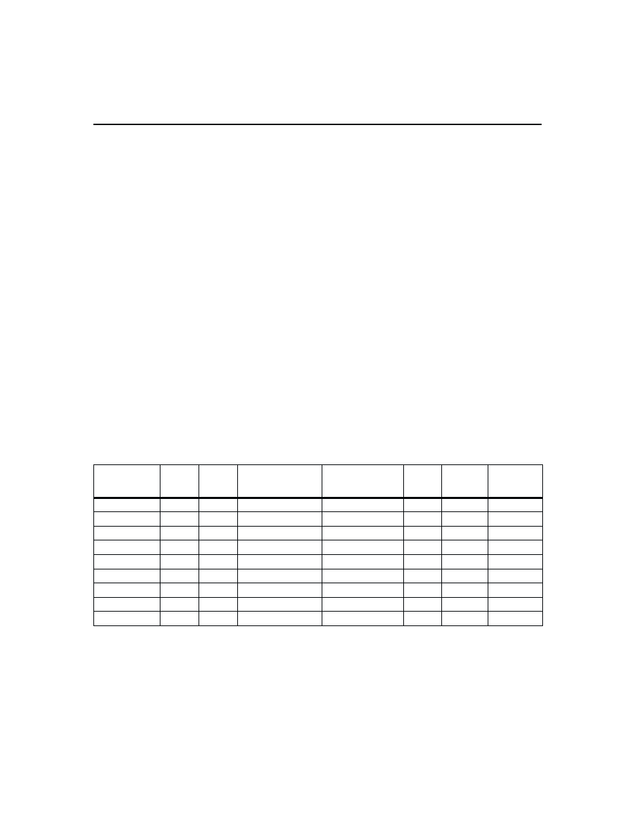
Table 1. Fast-Charge Safety Time/Hold-Off/Top-Off Table
bq2004
When the SNS voltage is greater than V
SNSHI
, the MOD
output is switched low--shutting off charging current to
the battery.
V
SNSLO
= 0.04
V
CC
± 25mV
V
SNSHI
= 0.05
V
CC
± 25mV
When used to gate an externally regulated current
source, the SNS pin is connected to V
SS
, and no sense re-
sisitor is required.
7
BD200401.eps
Timing
Control
OSC
Display
Control
Charge Control
State Machine
Discharge
Control
MOD
Control
TCO
Check
LTF
Check
A/D
EDV
Check
MCV
Check
DIS
MOD
INH
VCC VSS
BAT
SNS
TS
TCO
TM2
TM1
LED1
DCMD
DVEN
VTS - VSNS
VBAT - VSNS
LED2
DSEL
PWR
Control
Figure 3. Block Diagram
Mode 1
Charge Status
LED
1
LED
2
DSEL = V
SS
Battery absent
Low
Low
Fast charge pending or discharge-before-charge in progress
High
High
Fast charge in progress
Low
High
Charge complete, top-off, and/or trickle
High
Low
Mode 2
Charge Status
LED
1
LED
2
DSEL = Floating
Battery absent, fast charge in progress or complete
Low
Low
Fast charge pending
High
Low
Discharge in progress
Low
High
Top-off in progress
High
High
Mode 3
Charge Status
LED
1
LED
2
DSEL = V
CC
Battery absent
Low
Low
Fast charge pending or discharge-before-charge in progress
Low
1/8s high
1/8s low
Fast charge in progress
Low
High
Fast charge complete, top-off, and/or trickle
High
Low
Table 2. bq2004 LED Status Display Options
bq2004
8
Charge
Pending
DCMD Tied to Ground?
Rising Edge
on DCMD
Discharge-
Before-Charge
Pulse
Trickle
Charge
Pulse
Trickle
Charge
Pulse
Trickle
Charge
Pulse
Trickle
Charge
Top-Off
Charge
Fast
Charge
Battery Voltage?
Battery Temperature?
Top-Off
Selected?
New Charge Cycle Started by
Any One of:
VCC Rising to Valid Level
Battery Replacement
(VCELL Falling through VMCV)
Inhibit (INH) Released
VEDV < VCELL < VMCV
and
VHTF < VTEMP < VLTF*
VHTF < VTEMP < VLTF*
VEDV < VCELL < VMCV
VTEMP > VLTF or
VTEMP < VHTF
VCELL < VEDV
VCELL < VEDV
Yes
Yes
No
*VSEL = High disables LTF threshold enforcement
No
t > t
MCV
> VMCV
VCELL
> VMCV
VCELL
>
VCELL
VMCV
>
VCELL
VMCV
>
VCELL
VMCV
VCELL
<
VMCV
Charge
Complete
Battery
Absent
or Maximum
Time Out
VTEMP < VTCO
SD2004.eps
>
VCELL
VMCV
- V or
T/ t or
VTEMP
<
VTCO
or
Maximum Time Out
Figure 4. State Diagram
bq2004
9
Absolute Maximum Ratings
Symbol
Parameter
Minimum
Maximum
Unit
Notes
V
CC
V
CC
relative to V
SS
-0.3
+7.0
V
V
T
DC voltage applied on any pin ex-
cluding V
CC
relative to V
SS
-0.3
+7.0
V
T
OPR
Operating ambient temperature
-20
+70
∞C
Commercial
T
STG
Storage temperature
-55
+125
∞C
T
SOLDER
Soldering temperature
-
+260
∞C
10 sec max.
T
BIAS
Temperature under bias
-40
+85
∞C
Note:
Permanent device damage may occur if Absolute Maximum Ratings are exceeded. Functional opera-
tion should be limited to the Recommended DC Operating Conditions detailed in this data sheet. Expo-
sure to conditions beyond the operational limits for extended periods of time may affect device reliability.
DC Thresholds
(TA = TOPR; VCC
±10%)
Symbol
Parameter
Rating
Tolerance
Unit
Notes
V
SNSHI
High threshold at SNS result-
ing in MOD = Low
0.05 * V
CC
±0.025
V
V
SNSLO
Low threshold at SNS result-
ing in MOD = High
0.04 * V
CC
±0.010
V
V
LTF
Low-temperature fault
0.4 * V
CC
±0.030
V
V
TEMP
V
LTF
inhib-
its/terminates charge
V
HTF
High-temperature fault
(1/4 * V
LTF
) + (2/3 * V
TCO
)
±0.030
V
V
TEMP
V
HTF
inhibits
charge
V
EDV
End-of-discharge voltage
0.4 * V
CC
±0.030
V
V
CELL
< V
EDV
inhibits
fast charge
V
MCV
Maximum cell voltage
0.8 * V
CC
±0.030
V
V
CELL
> V
MCV
inhibits/
terminates charge
V
THERM
TS input change for
T/t
detection
-16
±4
mV
V
CC
= 5V, T
A
= 25
∞C
-
V
BAT input change for -
V
detection
-12
±4
mV
V
CC
= 5V, T
A
= 25
∞C
PVD
BAT input change for PVD
detection
-6
±2
mV
V
CC
= 5V, T
A
= 25
∞C
bq2004
10
Recommended DC Operating Conditions
(TA = TOPR)
Symbol
Condition
Minimum
Typical
Maximum
Unit
Notes
V
CC
Supply voltage
4.5
5.0
5.5
V
V
BAT
Battery input
0
-
V
CC
V
V
CELL
BAT voltage potential
0
-
V
CC
V
V
BAT
- V
SNS
V
TS
Thermistor input
0
-
V
CC
V
V
TEMP
TS voltage potential
0
-
V
CC
V
V
TS
- V
SNS
V
TCO
Temperature cutoff
0.2 * V
CC
-
0.4 * V
CC
V
Valid
T/t range
V
IH
Logic input high
2.0
-
-
V
DCMD, INH
Logic input high
V
CC
- 0.3
-
-
V
TM
1
, TM
2
, DSEL, VSEL
V
IL
Logic input low
-
-
0.8
V
DCMD, INH
Logic input low
-
-
0.3
V
TM
1
, TM
2
, DSEL, VSEL
V
OH
Logic output high
V
CC
- 0.8
-
-
V
DIS, MOD, LED
1
, LED
2
,
I
OH
-10mA
V
OL
Logic output low
-
-
0.8
V
DIS, MOD, LED
1
, LED
2
,
I
OL
10mA
I
CC
Supply current
-
1
3
mA
Outputs unloaded
I
SB
Standby current
-
-
1
µA
INH = V
IL
I
OH
DIS, LED
1
, LED
2
, MOD source
-10
-
-
mA
@V
OH
= V
CC
- 0.8V
I
OL
DIS, LED
1
, LED
2
, MOD sink
10
-
-
mA
@V
OL
= V
SS
+ 0.8V
I
L
Input leakage
-
-
±1
µA
INH, BAT, V = V
SS
to V
CC
Input leakage
50
-
400
µA
DCMD, V = V
SS
to V
CC
I
IL
Logic input low source
-
-
70
µA
TM
1
, TM
2
, DSEL, VSEL,
V = V
SS
to V
SS
+ 0.3V
I
IH
Logic input high source
-70
-
-
µA
TM
1
, TM
2
, DSEL, VSEL,
V = V
CC
- 0.3V to V
CC
I
IZ
Tri-state
-2
-
2
µA
TM
1
, TM
2
, DSEL, and VSEL
should be left disconnected
(floating) for Z logic input state
Note:
All voltages relative to V
SS
except as noted.
bq2004
11
Impedance
Symbol
Parameter
Minimum
Typical
Maximum
Unit
R
BAT
Battery input impedance
50
-
-
M
R
TS
TS input impedance
50
-
-
M
R
TCO
TCO input impedance
50
-
-
M
R
SNS
SNS input impedance
50
-
-
M
Timing
(TA = 0 to +70∞C; VCC
±10%)
Symbol
Parameter
Minimum
Typical
Maximum
Unit
Notes
t
PW
Pulse width for DCMD
and INH pulse command
1
-
-
µs
Pulse start for charge or discharge
before charge
d
FCV
Time base variation
-16
-
16
%
V
CC
= 4.75V to 5.25V
f
REG
MOD output regulation
frequency
-
-
300
kHz
t
MCV
Maximum voltage termi-
nation time limit
1
-
2
s
Time limit to distinguish battery re-
moved from charge complete.
Note:
Typical is at T
A
= 25∞C, V
CC
= 5.0V.
bq2004
12
bq2004
16-Pin DIP Narrow (PN)
16-Pin PN (0.300" DIP)
Dimension
Inches
Millimeters
Min.
Max.
Min.
Max.
A
0.160
0.180
4.06
4.57
A1
0.015
0.040
0.38
1.02
B
0.015
0.022
0.38
0.56
B1
0.055
0.065
1.40
1.65
C
0.008
0.013
0.20
0.33
D
0.740
0.770
18.80
19.56
E
0.300
0.325
7.62
8.26
E1
0.230
0.280
5.84
7.11
e
0.300
0.370
7.62
9.40
G
0.090
0.110
2.29
2.79
L
0.115
0.150
2.92
3.81
S
0.020
0.040
0.51
1.02
13
bq2004
16-Pin SOIC Narrow (SN)
A
A1
.004
C
B
e
D
E
H
L
16-Pin SN (0.150" SOIC)
Dimension
Inches
Millimeters
Min.
Max.
Min.
Max.
A
0.060
0.070
1.52
1.78
A1
0.004
0.010
0.10
0.25
B
0.013
0.020
0.33
0.51
C
0.007
0.010
0.18
0.25
D
0.385
0.400
9.78
10.16
E
0.150
0.160
3.81
4.06
e
0.045
0.055
1.14
1.40
H
0.225
0.245
5.72
6.22
L
0.015
0.035
0.38
0.89
14
bq2004
Data Sheet Revision History
Change No.
Page No.
Description
Nature of Change
1
10
Standby current ISB
Was 5
µA max; is 1 µA max
2
9
V
BSNSLO
Rating
Was: V
SNSHI
- (0.01 * V
CC
)
Is: 0.04 * V
CC
2
7
Correction in Peak Voltage Detect Termination section Was VCELL; is VBAT
2
3
Added block diagram
Diagram insertion
2
7
Added VSEL/termination table
Table insertion
2
8
Added values to Table 3
Top-off rate values
3
7
VSEL/Termination
Low, High changed
4
All
Revised and expanded format of this data sheet
Clarification
5
9
Corrected V
HTF
rating
Was: (1/3
V
LTF
) + (2/3
V
TCO
)
Is: (1/4
V
LTF
) + (3/4
V
TCO
)
6
9
T
OPR
Deleted industrial tempera-
ture range
Notes:
Change 1 = Apr. 1994 B "Final" changes from Dec. 1993 A "Preliminary."
Change 2 = Sept. 1996 C changes from Apr. 1994 B.
Change 3 = April 1997 C changes from Sept. 1996 C.
Change 4 = Oct. 1997 D changes from April 1997 C.
Change 5 = Jan. 1998 E changes from Oct. 1997 D.
Change 6 = June 1999 F changes from Jan. 1998 E.

15
bq2004
Ordering Information
bq2004
Package Option:
PN = 16-pin narrow plastic DIP
SN = 16-pin narrow SOIC
Device:
bq2004 Fast-Charge IC

16
IMPORTANT NOTICE
Texas Instruments and its subsidiaries (TI) reserve the right to make changes to their products or to discontinue any
product or service without notice, and advise customers to obtain the latest version of relevant information to verify,
before placing orders, that information being relied on is current and complete. All products are sold subject to the
terms and conditions of sale supplied at the time of order acknowledgement, including those pertaining to warranty,
patent infringement, and limitation of liability.
TI warrants performance of its semiconductor products to the specifications applicable at the time of sale in accor-
dance with TI's standard warranty. Testing and other quality control techniques are utilized to the extent TI deems
necessary to support this warranty. Specific testing of all parameters of each device is not necessarily performed, ex-
cept those mandated by government requirements.
CERTAIN APPLICATIONS USING SEMICONDUCTOR PRODUCTS MAY INVOLVE POTENTIAL RISKS OF DEATH,
PERSONAL INJURY, OR SEVERE PROPERTY OR ENVIRONMENTAL DAMAGE ("CRITICAL APPLICATIONS"). TI
SEMICONDUCTOR PRODUCTS ARE NOT DESIGNED, AUTHORIZED, OR WARRANTED TO BE SUITABLE FOR
USE IN LIFE-SUPPORT DEVICES OR SYSTEMS OR OTHER CRITICAL APPLICATIONS. INCLUSION OF TI
PRODUCTS IN SUCH APPLICATIONS IS UNDERSTOOD TO BE FULLY AT THE CUSTOMER'S RISK.
In order to minimize risks associated with the customer's applications, adequate design and operating safeguards
must be provided by the customer to minimize inherent or procedural hazards.
TI assumes no liability for applications assistance or customer product design. TI does not warrant or represent that
any license, either express or implied, is granted under any patent right, copyright, mask work right, or other intellec-
tual property right of TI covering or relating to any combination, machine, or process in which such semiconductor
products or services might be or are used. TI's publication of information regarding any third party's products or ser-
vices does not constitute TI's approval, warranty or endorsement thereof.
Copyright © 1999, Texas Instruments Incorporated