Features
Fast charge and conditioning of
nickel cadmium or nickel-metal
hydride batteries
Hysteretic PWM switch-mode
current regulation or gated con-
trol of an external regulator
Easily integrated into systems or
used as a stand-alone charger
Pre-charge qualification of tem-
perature and voltage
Configurable, direct LED outputs
display battery and charge status
Fast-charge termination by tem-
perature/
time, peak volume de-
tection, -
V, maximum voltage,
maximum temperature, and maxi-
mum time
Optional top-off charge and
pu ls ed cu rre nt mai nten anc e
charging
Logic-level controlled low-power
mode (< 5
µA standby current)
General Description
The bq2004 Fast Charge IC pro-
vides comprehensive fast charge con-
trol functions together with high-speed
switching power control circuitry on a
monolithic CMOS device.
Integration of closed-loop current
control circuitry allows the bq2004
to be the basis of a cost-effective so-
lution for stand-alone and system-
integrated chargers for batteries of
one or more cells.
Switch-activated discharge-before-
charge allows bq2004-based chargers
to support battery conditioning and
capacity determination.
High-efficiency power conversion is
accomplished using the bq2004 as a
hysteretic PWM controller for
switch-mode regulation of the charg-
ing current. The bq2004 may alterna-
tively be used to gate an externally
regulated charging current.
Fast charge may begin on applica-
tion of the charging supply, replace-
ment of the battery, or switch de-
pression. For safety, fast charge is
inhibited unless/until the battery
temperature and voltage are within
configured limits.
Temperature, voltage, and time are
monitored throughout fast charge.
Fast charge is terminated by any of
the following:
n
Rate of temperature time
(
T/ t)
n
Peak voltage detection (PVD)
n
Negative delta voltage (-
V)
n
Maximum voltage
n
Maximum temperature
n
Maximum time
After fast charge, optional top-off
and pulsed current maintenance
phases are available.
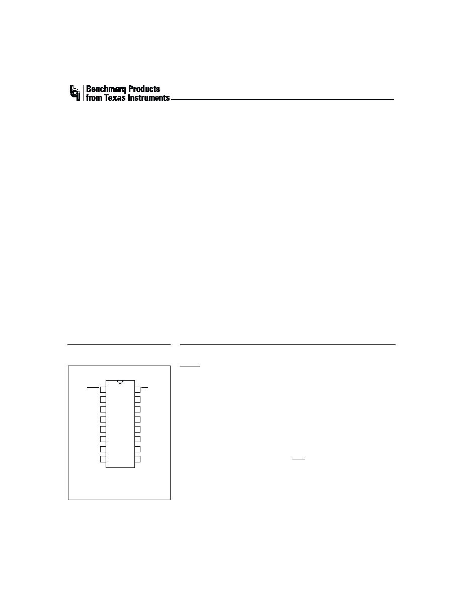
1
Fast-Charge IC
bq2004
DCMD
Discharge command
DSEL
Display select
VSEL
Voltage termination
select
TM
1
Timer mode select 1
TM
2
Timer mode select 2
TCO
Temperature cutoff
TS
Temperature sense
BAT
Battery voltage
1
PN2004E01.eps
16-Pin Narrow DIP
or Narrow SOIC
2
3
4
5
6
7
8
16
15
14
13
12
11
10
9
INH
DIS
MOD
VCC
VSS
LED2
LED1
SNS
DCMD
DSEL
VSEL
TM1
TM2
TCO
TS
BAT
SNS
Sense resistor input
LED
1
Charge status output 1
LED
2
Charge status output 2
V
SS
System ground
V
CC
5.0V
±10% power
MOD
Charge current control
DIS
Discharge control
output
INH
Charge inhibit input
Pin Connections
SLUS063A≠FEBRUARY 2001 G
Pin Names

Pin Descriptions
DCMD
Discharge-before-charge control input
The DCMD input controls the conditions
that enable discharge-before-charge. DCMD
is pulled up internally.
A negative-going
pulse on DCMD initiates a discharge to end-
of-discharge voltage (EDV) on the BAT pin,
followed by a new charge cycle start. Tying
D C M D t o g r o u n d e n a b l e s a u t o m a t i c
discharge-before-charge on every new charge
cycle start.
DSEL
Display select input
This three-state input configures the charge
status display mode of the LED
1
and LED
2
outputs. See Table 2.
VSEL
Voltage termination select input
This three-state input controls the voltage-
termination technique used by the bq2004.
When high, PVD is active.
When floating,
-
V is used. When pulled low, both PVD and
-
V are disabled.
TM
1
≠
TM
2
Timer mode inputs
TM
1
and TM
2
are three-state inputs that
configure the fast charge safety timer, voltage
termination hold-off time, "top-off", and
trickle charge control. See Table 1.
TCO
Temperature cut-off threshold input
Input to set maximum allowable battery
temperature.
If the potential between TS
and SNS is less than the voltage at the TCO
input, then fast charge or top-off charge is ter-
minated.
TS
Temperature sense input
Input, referenced to SNS,
for an external
thermister monitoring battery temperature.
BAT
Battery voltage input
BAT is the battery voltage sense input, refer-
enced to SNS.
This is created by a high-
impedance resistor-divider network con-
nected between the positive and the negative
terminals of the battery.
SNS
Charging current sense input
SNS controls the switching of MOD based on
an external sense resistor in the current
path of the battery. SNS is the reference po-
tential for both the TS and BAT pins.
If
SNS is connected to V
SS
, then MOD switches
high at the beginning of charge and low at
the end of charge.
LED
1
≠
LED
2
Charge status outputs
Push-pull outputs indicating charging
status. See Table 2.
V
SS
Ground
V
CC
V
CC
supply input
5.0V,
±10% power input.
MOD
Charge current control output
MOD is a push-pull output that is used to
control the charging current to the battery.
MOD switches high to enable charging cur-
rent to flow and low to inhibit charging
current flow.
DIS
Discharge control output
Push-pull output used to control an external
transistor to discharge the battery before
charging.
INH
Charge inhibit input
When low, the bq2004 suspends all charge
actions, drives all outputs to high imped-
ance, and assumes a low-power operational
state. When transitioning from low to high,
a new charge cycle is started.
2
bq2004
Functional Description
Figure 3 shows a block diagram and Figure 4 shows a
state diagram of the bq2004.
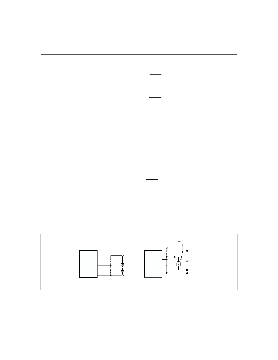
Battery Voltage and Temperature
Measurements
Battery voltage and temperature are monitored for
maximum allowable values. The voltage presented on
the battery sense input, BAT, should represent a
two-cell potential for the battery under charge.
A
resistor-divider ratio of:
RB1
RB2
=
N
2
- 1
is recommended to maintain the battery voltage within
the valid range, where N is the number of cells, RB1 is
the resistor connected to the positive battery terminal,
and RB2 is the resistor connected to the negative bat-
tery terminal. See Figure 1.
Note: This resistor-divider network input impedance to
end-to-end should be at least 200k
and less than 1M.
A ground-referenced negative temperature coefficient ther-
mistor placed in proximity to the battery may be used as a
low-cost temperature-to-voltage transducer. The tempera-
ture sense voltage input at TS is developed using a
resistor-thermistor network between V
CC
and V
SS
.
See
Figure 1. Both the BAT and TS inputs are referenced to
SNS, so the signals used inside the IC are:
V
BAT
- V
SNS
= V
CELL
and
V
TS
- V
SNS
= V
TEMP
Discharge-Before-Charge
The DCMD input is used to command discharge-before-
charge via the DIS output.
Once activated, DIS be-
comes active (high) until V
CELL
falls below V
EDV,
at
which time DIS goes low and a new fast charge cycle be-
gins.
The DCMD input is internally pulled up to V
CC
(its inac-
tive state). Leaving the input unconnected, therefore,
results in disabling discharge-before-charge. A negative
going pulse on DCMD initiates discharge-before-charge
at any time regardless of the current state of the
bq2004.
If DCMD is tied to V
SS
, discharge-before-
charge will be the first step in all newly started charge
cycles.
Starting a Charge Cycle
A new charge cycle (see Figure 2) is started by:
1.
V
CC
rising above 4.5V
2.
V
CELL
falling through the maximum cell voltage,
V
MCV
where:
V
MCV
= 0.8
V
CC
± 30mV
3.
A transition on the INH input from low to high.
If DCMD is tied low, a discharge-before-charge is exe-
cuted as the first step of the new charge cycle. Other-
wise, pre-charge qualification testing is the first step.
The battery must be within the configured temperature
and voltage limits before fast charging begins.
The valid battery voltage range is V
EDV
< V
BAT
< V
MCV
where:
V
EDV
= 0.4
V
CC
± 30mV
3
bq2004
Fg2004a.eps
N
T
C
bq2004
VCC
PACK +
PACK -
TS
SNS
RT1
RT2
RB2
RB1
bq2004
Negative Temperature
Coefficient Thermister
PACK+
PACK-
BAT
SNS
Figure 1. Voltage and Temperature Monitoring
4
Fast Charging
Top-Off
(Optional)
TD200401a.eps
Dis-
charge
(Optional)
Charge
Pending*
(Pulse-Trickle)
DIS
MOD
MOD
Mode 1, LED2 Status Output
Discharge-Before-Charge started
or
Battery discharged to 0.4
*
VCC. Battery outside
temperature/voltage limits.
Battery within temperature/voltage limits.
Pulse-Trickle
Switch-mode
Configuration
External
Regulation
(
SNS Grounded)
Mode 1, LED1 Status Output
Mode 2, LED2 Status Output
Mode 2, LED1 Status Output
Mode 3, LED2 Status Output
Mode 3, LED1 Status Output
260 s
2080 s
260 s
2080 s
260 s
Note*
260 s
Note*
*See Table 3 for pulse-trickle period.
Figure 2. Charge Cycle Phases
bq2004
The valid temperature range is V
HTF
< V
TEMP
< V
LTF
,
where:
V
LTF
= 0.4
V
CC
± 30mV
V
HTF
= [(1/4
V
LTF
) + (3/4
V
TCO
)]
± 30mV
Note: The low temperature fault (LTF) threshold is not
enforced if
the IC is configured for PVD termination
(VSEL = high).
V
TCO
is the voltage presented at the TCO input pin, and is
configured by the user with a resistor divider between V
CC
and ground. The allowed range is 0.2 to 0.4
V
CC
.
If the temperature of the battery is out of range, or the
voltage is too low, the chip enters the charge pending
state and waits for both conditions to fall within their al-
lowed limits. The MOD output is modulated to provide
the configured trickle charge rate in the charge pending
state.
There is no time limit on the charge pending
state; the charger remains in this state as long as the
voltage or temperature conditons are outside of the al-
lowed limits. If the voltage is too high, the chip goes to
the battery absent state and waits until a new charge
cycle is started.
Fast charge continues until termination by one or more
of the six possible termination conditions:
n
Delta temperature/delta time (
T/t)
n
Peak voltage detection (PVD)
n
Negative delta voltage (-
V)
n
Maximum voltage
n
Maximum temperature
n
Maximum time
PVD and - V Termination
The bq2004 samples the voltage at the BAT pin once
every 34s. When -
V termination is selected, if V
CELL
is
lower than any previously measured value by 12mV
±4mV (6mV/cell), fast charge is terminated. When PVD
termination is selected, if V
CELL
is lower than any previ-
ously measured value by 6mV
±2mV (3mV/cell), fast
charge is terminated. The PVD and -
V tests are valid
in the range 0.4
V
CC
< V
CELL
< 0.8
V
CC
.
Voltage Sampling
Each sample is an average of voltage measurements
taken 57
µs apart. The IC takes 32 measurements in
PVD mode and 16 measurements in -
V mode. The re-
sulting sample periods (9.17ms and 18.18ms, respec-
tively) filter out harmonics centered around 55Hz and
109Hz. This technique minimizes the effect of any AC
line ripple that may feed through the power supply from
either 50Hz or 60Hz AC sources. Tolerance on all tim-
ing is
±16%.
Voltage Termination Hold-off
A hold-off period occurs at the start of fast charging.
During the hold-off period, -
V termination is disabled.
This avoids premature termination on the voltage
spikes sometimes produced by older batteries when
fast-charge current is first applied.
T/t, maximum
voltage and maximum temperature terminations are
not affected by the hold-off period.
T/ t Termination
The bq2004 samples at the voltage at the TS pin every
34s, and compares it to the value measured two samples
earlier. If V
TEMP
has fallen 16mV
±4mV or more, fast
charge is terminated. If VSEL = high, the
T/t termi-
nation test is valid only when V
TCO
< V
TEMP
< V
TCO
+
0.2
V
CC
. Otherwise the
T/t termination test is valid
only when V
TCO
< V
TEMP
< V
LTF
.
Temperature Sampling
Each sample is an average of 16 voltage measurements
taken 57
µs apart. The resulting sample period
(18.18ms) filters out harmonics around 55Hz. This tech-
nique minimizes the effect of any AC line ripple that
may feed through the power supply from either 50Hz or
60Hz AC sources. Tolerance on all timing is
±16%.
Maximum Voltage, Temperature, and Time
Anytime V
CELL
rises above V
MCV,
the LEDs go off and
charging ceases immediately. If V
CELL
then falls back be-
low V
MCV
before t
MCV
= 1.5s
±0.5s, the chip transitions to
the Charge Complete state (maximum voltage termina-
tion). If V
CELL
remains above V
MCV
at the expiration of
t
MCV,
the bq2004 transitions to the Battery Absent state
(battery removal). See Figure 4.
Maximum temperature termination occurs anytime
V
TEMP
falls below the temperature cutoff threshold
V
TCO
.
Unless PVD termination is enabled (VSEL =
high), charge will also be terminated if V
TEMP
rises
above the low temperature fault threshold, V
LTF
, after
fast charge begins. The V
LTF
threshold is not enforced
when the IC is configured for PVD termination.
Maximum charge time is configured using the TM pin.
Time settings are available for corresponding charge
rates of C/4, C/2, 1C, and 2C. Maximum time-out termi-
nation is enforced on the fast-charge phase, then reset,
5
bq2004
VSEL Input
Voltage Termination
Low
Disabled
Float
-
V
High
PVD