Gas Gauge IC for High Discharge Rates (Rev. A)
bq2016
GAS GAUGE IC FOR
HIGH DISCHARGE RATES
SLUS475A JANUARY 2001 REVISED NOVEMBER 2002
1
POST OFFICE BOX 655303
·
DALLAS, TEXAS 75265
D
Provides Accurate Measurement of
Available Capacity in Nicd or NiMH
Batteries
D
Measures a Wide Dynamic-Current Range
D
Requires
1 Square Inch of PCB Space for
Easy Pack Integration
D
Measures Charge Flow Using a Low-Offset
V-to-F Converter
D
Automatically Compensates Measurements
for Rate and Temperature
D
Supports 5 LEDs for Remaining Capacity
Indication
D
Provides a 1-Wire HDQ Communication
Interface
D
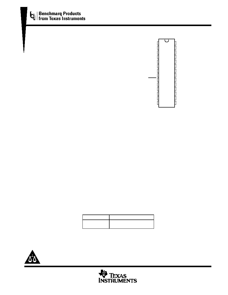
Packaging: 28-Pin SSOP
description
The bq2016 gas gauge IC for battery pack or in-system installation maintains an accurate record of available
battery capacity. To integrate charge and discharge activity of the battery, the IC monitors a voltage drop across
a sense resistor connected in series with the cells of the battery. The bq2016 compensates for battery
temperature, charge/discharge rate, and battery self-discharge to the charge counter to provide available-
capacity information across a wide range of operating conditions. The bq2016 works with NiCd or NiMH battery
packs that have a capacity of 1 to 4.5 Ah and that are designed for high discharge rate applications such as
power tools.
The VPFC input sets the initial full charge reference of the battery pack. The bq2016 learns the true discharge
capacity of the battery pack and automatically updates the full-charge reference during the course of a
discharge cycle from full to empty. The remaining capacity is reported as the ratio between the actual discharge
capacity and the full-charge capacity. The bq2016 communicates available capacity using 5 LEDs or the 1-wire
communications port.
The 1-wire serial communication port (5Kb/s) allows an external processor to read and write the internal
registers of the bq2016. Communication with the bq2016 is useful for pack testing or host processing of the
available battery information. The internal registers include available battery capacity, voltage, temperature,
current, and battery status. The RBI input maintains the register set in the event of pack voltage collapse due
to a high discharge pulse.
The bq2016 circuit can operate from the cells in the pack. The REG output and an external FET provide a simple,
inexpensive voltage regulator to supply power to the circuit from the cells
OPTIONS
TJ
28-PIN SSOP PACKAGE
20
°
C to 70
°
C
bq2016DBQ
bq2016DBQR
Copyright
2002, Texas Instruments Incorporated
PRODUCTION DATA information is current as of publication date.
Products conform to specifications per the terms of Texas Instruments
standard warranty. Production processing does not necessarily include
testing of all parameters.
Please be aware that an important notice concerning availability, standard warranty, and use in critical applications of
Texas Instruments semiconductor products and disclaimers thereto appears at the end of this data sheet.
1
2
3
4
5
6
7
8
9
10
11
12
13
14
28
27
26
25
24
23
22
21
20
19
18
17
16
15
HDQ
NC
NC
RBI
REG
NC
V
CC
V
SS
DISP
LED1
LED2
LED3
LED4
LED5
NC
NC
SB
PROG
VPFC
NC
SR1
SR2
SRC
TS
THON
CVON
NC
NC
TSSOP PACKAGE
(TOP VIEW)
NC -- Do not connect
bq2016
GAS GAUGE IC FOR
HIGH DISCHARGE RATES
SLUS475A JANUARY 2001 REVISED NOVEMBER 2002
2
POST OFFICE BOX 655303
·
DALLAS, TEXAS 75265
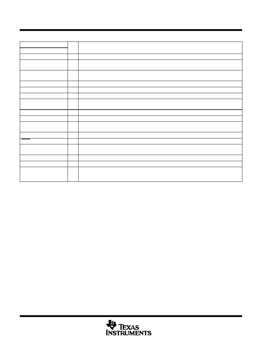
Terminal Functions
TERMINAL
I/O
DESCRIPTION
NAME
NO.
I/O
DESCRIPTION
HDQ
1
I/O
Serial communication input/output. Open-drain bidirectional communications port.
RBI
4
I
Register backup input provides backup potential to the bq2016 registers during periods of low operating
voltage. RBI accepts a storage capacitor or a battery input.
REG
5
O
Regulator output provides a reference to control an n-JFET for VCC regulation to the bq2016 from the
battery potential.
VCC
7
I
Supply voltage input
VSS
8
Ground
LED1LED5
1014
O
LED display segment outputs that each may drive an external LED.
CVON
17
O
Cell voltage divider control. Output to connect the voltage divider on the voltage input during
measurement.
VPFC
24
I
Program capacity input. 16-level input to program the initial battery full-charge reference.
SB
26
I
Battery voltage input. Input connection to monitor batterypack voltage.
SR2SR1
21,22
I
Sense resistor inputs. Input connections for a small value sense resistor to monitor the battery charge and
discharge current flow.
SRC
20
I
Current sense voltage input to monitor instantaneous current.
DISP
9
I
Display activation input that activates the LED drivers LED1LED5.
TS
19
I
Temperature sense input connects to an external thermistor or should be grounded when using the internal
thermistor. The function depends on the state of the PROG input.
PROG
25
I
Program input defines the temperature measurement thermistor (internal or external).
THON
18
O
Thermistor bias control output to control a switch in series with an optional external thermistor.
NC
2, 3, 6, 15,
16, 23, 27,
28
Do not connect. For proper device operation, these pins should not be connected.
bq2016
GAS GAUGE IC FOR
HIGH DISCHARGE RATES
SLUS475A JANUARY 2001 REVISED NOVEMBER 2002
3
POST OFFICE BOX 655303
·
DALLAS, TEXAS 75265
absolute maximum ratings over operating free-air temperature range (unless otherwise noted)
Relative to V
SS
: V
CC
0.3 V to 6 V
. . . . . . . . . . . . . . . . . . . . . . . . . . . . . . . . . . . . . . . . . . . . . . . . . . . . . . . . . . . . . .
V
IN
(All other pins)
0.3 V to 6 V
. . . . . . . . . . . . . . . . . . . . . . . . . . . . . . . . . . . . . . . . . . . . . . . . .
Operating temperature, T
OPR
20
°
C to 70
°
C
. . . . . . . . . . . . . . . . . . . . . . . . . . . . . . . . . . . . . . . . . . . . . . . . . . . . . .
Stresses beyond those listed under "absolute maximum ratings" may cause permanent damage to the device. These are stress ratings only, and
functional operation of the device at these or any other conditions beyond those indicated under "recommended operating conditions" is not
implied. Exposure to absolute-maximum-rated conditions for extended periods may affect device reliability.
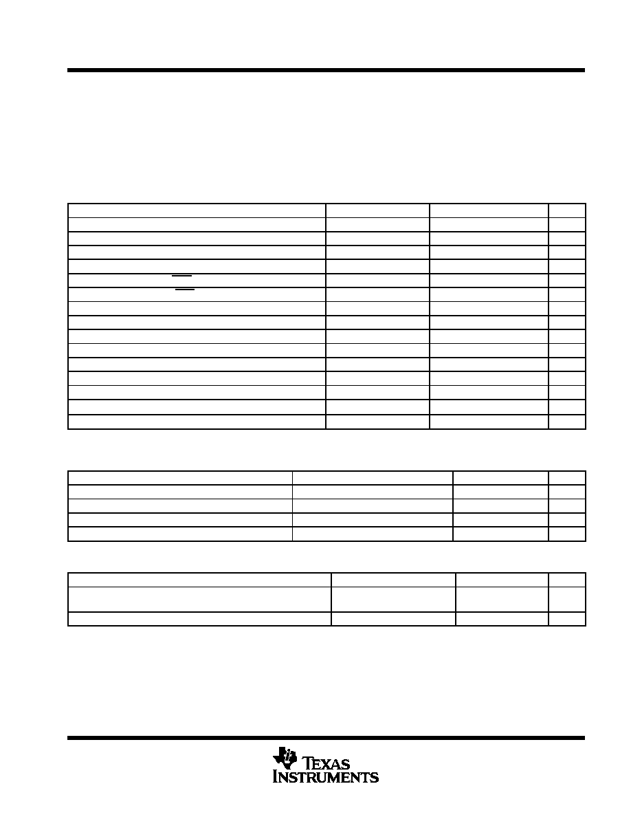
dc electrical characteristics
PARAMETER
TEST CONDITIONS
MIN
TYP
MAX
UNIT
VCC
Supply voltage
2.7
3.3
3.7
V
ICC
Operating current
180
235
µ
A
VOLS
Sink voltage: LED1LED5
IOLS = 5 mA
0.4
V
VOLS
Sink voltage: TI ION, CVON
IOLS = 1 mA
0.36
V
VIL
Input voltage low DISP
0.3
0.8
V
VIH
Input voltage high DISP
2.0
V
CC
+ 0.3
V
VOL
Output voltage low HDQ
IOL = 1 mA
0.4
V
VILS
Input voltage low HDQ
0.3
0.8
V
VIHS
Input voltage high HDQ
1.7
6.0
V
VAI
Input voltage range SB, PROG, VPFC, TS
VSS0.3
VCC + 0.3
V
IRB
RBI data-retention input current
VRBI
>
3 V, VCC
<
2 V
10
50
nA
VRBI
RBI data-retention voltage
1.3
V
ZAI1
Input impedance: SR1, SR2
01.25V
10
M
ZAI2
Input impedance: SB, SRC
01.25V
5
M
ZAI3
Input impedance: PROG, VPFC
0VCC
5
M
NOTE: ZAI specifications are reference numbers based on process data.
VFC characteristics, V
CC
= 3.13.5 V, T
OPR
= 0
°
C to 70
°
C (unless otherwise noted)
PARAMETER
TEST CONDITIONS
MIN
TYP
MAX
UNIT
VSR
Input voltage range, VSR2 and VSR1
VSR = VSR2 VSR1
0.25
0.25
V
VSROS
VSR input offset
VSR2 = VSR1, autocorrection disabled
300
50
300
µ
V
VSRCOS
Calibrated offset
After autocorrection
16
16
V
INL
Integral nonlinearity error
TOPR = 0
°
C to 50
°
C
0.21%
REG characteristics
PARAMETER
TEST CONDITIONS
MIN
TYP
MAX
UNIT
VRO
REG controlled output voltage
JFET: Rds(on)
<
150
Vgs (off)
<
3 V at 10
µ
A
3.1
3.3
3.5
V
IREG
REG output current
1
µ
A
bq2016
GAS GAUGE IC FOR
HIGH DISCHARGE RATES
SLUS475A JANUARY 2001 REVISED NOVEMBER 2002
4
POST OFFICE BOX 655303
·
DALLAS, TEXAS 75265
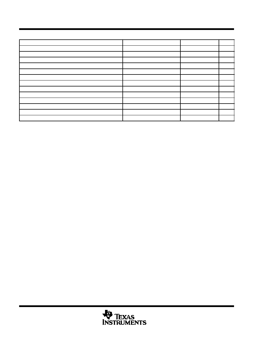
serial communication timing parameters
PARAMETER
TEST CONDITIONS
MIN
TYP
MAX
UNIT
t(CYCH)
Cycle time, host to bq2016 (write)
190
µ
s
t(CYCB)
Cycle time, bq2016 to host (read)
190
205
250
µ
s
t(STRH)
Start hold, host to bq2016 (write)
5
ns
t(STRB)
Start hold, bq2016 to host (read)
32
µ
s
t(DSU)
Data setup time
50
µ
s
t(DSUB)
Data setup time
50
µ
s
t(DH)
Data hold time
90
µ
s
t(DV)
Data valid time
80
µ
s
t(SSU)
Stop setup time
145
µ
s
t(SSUB)
Stop setup time
145
µ
s
t(RSPS)
Response time, bq2016 to host
320
µ
s
t(B)
Break
190
µ
s
t(BR)
Break recovery
40
µ
s
bq2016
GAS GAUGE IC FOR
HIGH DISCHARGE RATES
SLUS475A JANUARY 2001 REVISED NOVEMBER 2002
5
POST OFFICE BOX 655303
·
DALLAS, TEXAS 75265
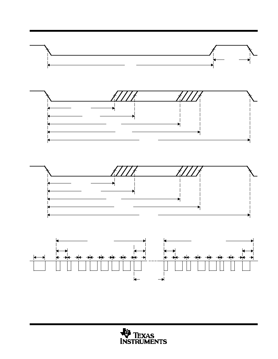
timing requirements
t(B)
t(BR)
Figure 1. Break Timing
t(CYCH)
t(STRH)
t(DSU)
t(DH)
t(SSU)
Write 0
Write 1
Figure 2. Host to bq2016
t(CYCB)
t(STRB)
t(DSUB)
t(DV)
t(SSUB)
Read 0
Read 1
Figure 3. bq2016 to Host
Break
Written by Host to bq2016
LSB
MSB
1
1
0
0
0
0
0
0
03h = 00000011
MSB
LSB
Received by Host from bq2016
1
0
1
0
0
1
1
0
65h = 0 1 1 0 0 1 0 1
MSB
LSB
0
1
2
3
4
5
6
7
CMDR = 03h
LSB
MSB
0
1
2
3
4
5
6
7
Data (NAC) = 65h
t(RSPS)
Figure 4. Typical Communication With the bq2016
Document Outline
- features
- description
- Terminal Functions
- absolute maximum ratings over operating free-air temperature range (unl\
ess otherwise noted)
- dc electrical characteristics
- VFC characteristics, V CC = 3.1
3.5 V, T OPR = 0C to 70C (unless otherw\
ise noted)
- REG characteristics
- serial communication timing parameters
- timing requirements
- functional description
- general operation
- measurements
- charge and discharge counting
- digital filter and VFC calibration
- voltage monitoring and thresholds
- current
- temperature
- gas gauge operation
- main gas gauge registers
- programmed full count (PFC)
- nominal available capacity (NAC)
- NAC calibration
- last measured discharge (LMD)
- discharge count register (DCR)
- programming the bq2016
- programmable configuration settings
- design capacity
- internal or external thermistor
- programming example
- charge and discharge count counting
- charge counting
- discharge counting
- self-discharge estimation
- count compensations
- charge compensations
- discharge compensation
- error summary
- capacity inaccurate
- display
- RBI input
- initialization
- communicating with the bq2016
- command code and registers
- command code
- registers
- FLAGS1 (0x01)
Primary Status Flags
- CHGS
- BRP
- MCV
- CI
- VDQ
- EDV
- TEMP (0x02)
Temperature
- NAC (0x03)
Nominal Available Capacity
- LMD (0x05)
Last Measured Discharge
- FLAGS2 (0x06)
Second Status Flags
- DR2
0
- OVLD
- VPFC (0x07)
VPFC Pin Input Level
- VPROG (0x08)
VPROG Pin Input Level
- CPI (0x09)
Capacity Input Level
- OCTL (0x0a)
Output Control
- FULCNT (0x0b)
Full Count Register
- CMDWD (0x0c)
Command Word
- PFC (0x0f)
Programmed Full Count
- VSB (0x10 and 0x11)
Battery Voltage
- VSR (0x12 and 0x13)
Current Scale
- TEMPV (0x14 and 0x15)
Thermistor Voltage
- DCR (0x18)
Discharge Count Register
- FLAGS3 (0x4c)
Third Status Flags
- CR1
CR0
- VQ
- APPLICATION INFORMATION
- bq2016 applications schematic
- IMPORTANT NOTICE