
Features
Conforms to battery manufactur-
ers' charge recommendations for
cyclic and float charge
Pin-selectable charge algorithms
-
Two-Step Voltage with
temperature-compensated
constant-voltage maintenance
-
Two-Step Current with
constant-rate pulsed current
maintenance
-
Pulsed Current: hysteretic,
on-demand pulsed current
Pin-selectable charge termination
by maximum voltage,
2
V, mini-
mum current, and maximum
time
Pre-charge qualification detects
shorted, opened, or damaged cells
and conditions battery
Charging continuously qualified by
temperature and voltage limits
Internal temperature-compen-
sated voltage reference
Pulse-width modulation control
-
Ideal for high-efficiency
switch-mode power conversion
-
Configurable for linear or
gated current use
Direct LED control outputs dis-
play charge status and fault con-
ditions
General Description
The bq2031 Lead-Acid Fast Charge
IC is designed to optimize charging
of lead-acid chemistry batteries. A
flexible pulse-width modulation
regulator allows the bq2031 to con-
trol constant-voltage, constant-
current, or pulsed-current charging.
The regulator frequency is set by an
external capacitor for design flexi-
bility. The switch-mode design keeps
power dissipation to a minimum for
high charge current applications.
A charge cycle begins when power is
applied or the battery is replaced.
For safety, charging is inhibited un-
til the battery voltage is within con-
figured limits. If the battery voltage is
less than the low-voltage threshold,
the bq2031 provides trickle-current
charging until the voltage rises into
the allowed range or an internal
t i m e r r u n s o u t a n d p l a c e s t h e
bq2031 in a Fault condition. This
procedure prevents high-current
charging of cells that are possibly
damaged or reversed. Charging is
inhibited anytime the temperature
of the battery is outside the config-
urable, allowed range. All voltage
t h r e s h o l d s
a r e
t e m p e r a t u r e -
compensated.
The bq2031 terminates fast (bulk)
charging based on the following:
I
Maximum voltage
I
Second difference of cell voltage
(
2
V)
I
Minimum current (in constant-
voltage charging)
I
Maximum time-out (MTO)
After bulk charging, the bq2031 pro-
vides temperature-compensated
maintenance (float) charging to
maintain battery capacity.
1
Lead-Acid Fast-Charge IC
TMTO
Time-out timebase input
FLOAT
State control output
BAT
Battery voltage input
VCOMP
Voltage loop comp input
ICOMP
Current loop comp input
IGSEL
Current gain select input
SNS
Sense resistor input
TS
Temperature sense input
TPWM
Regulator timebase input
1
PN203101.eps
16-Pin Narrow
DIP or SOIC
2
3
4
5
6
7
8
16
15
14
13
12
11
10
9
LED2/DSEL
LED1/TSEL
MOD
VCC
VSS
COM
LED3/QSEL
TPWM
TMTO
FLOAT
BAT
VCOMP
ICOMP
IGSEL
SNS
TS
LED
3
/
Charge status output 3/
QSEL
Charge algorithm select
input 1
COM
Common LED output
V
SS
System ground
V
CC
5.0V
±10% power
MOD
Modulation control
output
LED
1
/
Charge status output 1/
TSEL
Charge algorithm select
input 2
LED
2
/
Charge status output 2/
DSEL
Display select input
Pin Connections
Pin Names
SLUS156≠JUNE 1999 E
bq2031

Pin Descriptions
TMTO
Time-out timebase input
This input sets the maximum charge time.
The resistor and capacitor values are deter-
mined using equation 6. Figure 9 shows the
resistor/capacitor connection.
FLOAT
Float state control output
This open-drain output uses an external re-
sistor divider network to control the BAT in-
put voltage threshold (V
FLT
) for the float
charge regulation. See Figure 1.
BAT
Battery voltage input
BAT is the battery voltage sense input. This po-
tential is generally developed using a high-
impedance resistor divider network connected
between the positive and the negative terminals
of the battery. See Figure 6 and equation 2.
VCOMP
Voltage loop compensation input
This input uses an external C or R-C net-
work for voltage loop stability.
IGSEL
Current gain select input
This three-state input is used to set I
MIN
for
fast charge termination in the Two-Step
Voltage algorithm and for maintenance cur-
rent regulation in the Two-Step Current al-
gorithm. See Tables 3 and 4.
ICOMP
Current loop compensation input
This input uses an external C or R-C net-
work for current loop stability.
SNS
Charging current sense input
Battery current is sensed via the voltage de-
veloped on this pin by an external sense re-
sistor, R
SNS
, connected in series with the low
side of the battery. See equation 8.
TS
Temperature sense input
This input is for an external battery tem-
perature monitoring thermistor or probe. An
external resistor divider network sets the
lower and upper temperature thresholds.
See Figures 7 and 8 and equations 4 and 5.
TPWM
Regulation timebase input
This input uses an external timing capacitor
to ground the pulse-width modulation
(PWM) frequency. See equation 9.
COM
Common LED output
Common output for LED
1≠3
. This output is
in a high-impedance state during initiali-
zation to read program inputs on TSEL,
QSEL, and DSEL.
QSEL
Charge regulation select input
With TSEL, selects the charge algorithm.
See Table 1.
MOD
Current-switching control output
MOD is a pulse-width modulated push/pull
output that is used to control the charging
current to the battery. MOD switches high
to enable current flow and low to inhibit cur-
rent flow.
LED
1≠3
Charger display status 1≠3 outputs
These charger status output drivers are for
the direct drive of the LED display. Display
modes are shown in Table 2. These outputs are
tri-stated during initialization so that QSEL,
TSEL, and DSEL can be read.
DSEL
Display select input
This three-level input controls the LED
1≠3
charge display modes. See Table 2.
TSEL
Termination select input
With QSEL, selects the charge algorithm.
See Table 1.
V
CC
V
CC
supply
5.0V,
± 10% power
V
SS
Ground
Functional Description
The bq2031 functional operation is described in terms of:
n
Charge algorithms
n
Charge qualification
n
Charge status display
n
Voltage and current monitoring
n
Temperature monitoring
2
bq2031

n
Fast charge termination
n
Maintenance charging
n
Charge regulation
Charge Algorithms
Three charge algorithms are available in the bq2031:
n
Two-Step Voltage
n
Two-Step Current
n
Pulsed Current
The state transitions for these algorithms are described
in Table 1 and are shown graphically in Figures 2
through 4. The user selects a charge algorithm by con-
figuring pins QSEL and TSEL.
Charge Qualification
The bq2031 starts a charge cycle when power is applied
while a battery is present or when a battery is inserted.
Figure 1 shows the state diagram for pre-charge qualifi-
cation and temperature monitoring. The bq2031 first
checks that the battery temperature is within the al-
lowed, user-configurable range. If the temperature is
out-of-range (or the thermistor is missing), the bq2031
enters the Charge Pending state and waits until the bat-
tery temperature is within the allowed range. Charge
Pending is annunciated by LED
3
flashing.
3
bq2031
Algorithm/State
QSEL
TSEL
Conditions
MOD Output
Two-Step Voltage
L
H/L
Note 1
-
-
Fast charge, phase 1
while V
BAT
< V
BLK
, I
SNS
= I
MAX
Current regulation
Fast charge, phase 2
while I
SNS
> I
MIN
, V
BAT
= V
BLK
Voltage regulation
Primary termination
I
SNS
= I
MIN
Maintenance
V
BAT
= V
FLT
Voltage regulation
Two-Step Current
H
L
-
-
Fast charge
while V
BAT
< V
BLK
, I
SNS
= I
MAX
Current regulation
Primary termination
V
BAT
= V
BLK
or
2
V < -8mV
Note 2
Maintenance
I
SNS
pulsed to average I
FLT
Fixed pulse current
Pulsed Current
H
H
-
-
Fast charge
while V
BAT
< V
BLK
, I
SNS
= I
MAX
Current regulation
Primary termination
V
BAT
= V
BLK
Maintenance
I
SNS
= I
MAX
after V
BAT
= V
FLT
;
I
SNS
= 0 after V
BAT
= V
BLK
Hysteretic pulsed
current
Notes:
1.
May be high or low, but do not float.
2.
A Unitrode proprietary algorithm for accumulating successive differences between samples of V
BAT
.
Table 1. bq2031 Charging Algorithms
Chip On
VCC 4.5V
Temperature
Checks On
Battery
Status?
Temperature
in Range
Temperature Out
of Range or
Thermistor Absent
Voltage
Regulation
@ VFLT +
0.25V
Bulk
Charge
Fault
LED3 = 1
MOD = 0
Charge
Pending
LED3 Flash
MOD = 0
Current
Regulation
@ICOND
Temperature Out
of Range or
Thermistor Absent
Temperature In
Range, Return
to Original State
VCELL < VLCO or
VCELL > VHCO
VCELL VLCO or
Fail:
t = tQT1 or
VCELL > VHCO
Present
VLCO < VCELL < VHCO
ISNS < ICOND
VCELL < VMIN
FG203101.eps
Test 1
VCELL VHCO
PASS: ISNS ICOND
>
Test 2
PASS: VCELL VMIN
>
Fast
Charge
VCELL < VMIN
Termination
Fail:
t = tQT2 or
VCELL < VLCO or
VCELL > VHCO
Absent
VCELL < VLCO or
VCELL > VHCO
Figure 1. Cycle Start/Battery
Qualification State Diagram

Thermal monitoring continues throughout the charge
cycle, and the bq2031 enters the Charge Pending state
anytime the temperature is out of range. (There is one
exception; if the bq2031 is in the Fault state--see be-
low--the out-of-range temperature is not recognized un-
til the bq2031 leaves the Fault state.)
All timers are
suspended (but not reset) while the bq2031 is in Charge
Pending. When the temperature comes back into range,
the bq2031 returns to the point in the charge cycle
where the out-of-range temperature was detected.
When the temperature is valid, the bq2031 performs two
tests on the battery. In test 1, the bq2031 regulates a voltage
of V
FLT
+ 0.25V across the battery and observes I
SNS
. If I
SNS
does not rise to at least I
COND
within a time-out period (e.g.,
the cell has failed open), the bq2031 enters the Fault state. If
test 1 passes, the bq2031 then regulates current to I
COND
(=
I
MAX
/5) and watches V
CELL
(= V
BAT
- V
SNS
). If V
CELL
does
not rise to at least V
FLT
within a time-out period (e.g., the cell
has failed short), again the bq2031 enters the Fault state. A
hold-off period is enforced at the beginning of qualification
test 2 before the bq2031 recognizes its "pass" criterion. If this
second test passes, the bq2031 begins fast (bulk) charging.
Once in the Fault state, the bq2031 waits until V
CC
is cy-
cled or a battery insertion is detected. It then starts a new
charge cycle and begins the qualification process again.
Charge Status Display
Charge status is annunciated by the LED driver outputs
LED
1
≠LED
3
. Three display modes are available in the bq2031;
the user selects a display mode by configuring pin DSEL. Table
2 shows the three modes and their programming pins.
The bq2031 does not distinguish between an over-voltage
fault and a "battery absent" condition. The bq2031 enters
the Fault state, annunciated by turning on LED
3
, when-
ever the battery is absent. The bq2031, therefore, gives an
indication that the charger is on even when no battery is
in place to be charged.
4
bq2031
Mode
Charge Action State
LED
1
LED
2
LED
3
DSEL = 0
(Mode 1)
Battery absent or over-voltage fault
Low
Low
High
Pre-charge qualification
Flash
Low
Low
Fast charging
High
Low
Low
Maintenance charging
Low
High
Low
Charge pending (temperature out of range)
X
X
Flash
Charging fault
X
X
High
DSEL = 1
(Mode 2)
Battery absent or over-voltage fault
Low
Low
High
Pre-charge qualification
High
High
Low
Fast charge
Low
High
Low
Maintenance charging
High
Low
Low
Charge pending (temperature out of range)
X
X
Flash
Charging fault
X
X
High
DSEL = Float
(Mode 3)
Battery absent or over-voltage fault
Low
Low
High
Pre-charge qualification
Flash
Flash
Low
Fast charge: current regulation
Low
High
Low
Fast charge: voltage regulation
High
High
Low
Maintenance charging
High
Low
Low
Charge pending (temperature out of range)
X
X
Flash
Charging fault
X
X
High
Notes:
1 = V
CC
; 0 = V
SS
; X = LED state when fault occurred; Flash =
1
6
s low,
1
6
s high.
In the Pulsed Current algorithm, the bq2031 annunciates maintenance when charging current is off and
fast charge whenever charging current is on.
Table 2. bq2031 Display Output Summary
5
bq2031
IFLT
IMIN
ICOND
IMAX
Current
Voltage
VMIN
VFLT
VBLK
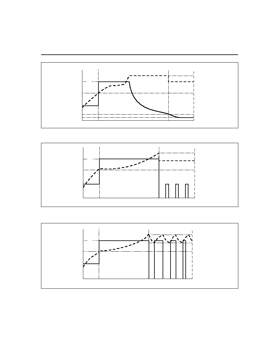
Time
Phase 1
Fast Charge
Phase 2
Current
Voltage
Maintenance
Qualification
Figure 2. Two-Step Voltage Algorithm
ICOND
IMAX
Current
Voltage
VMIN
VFLT
VBLK
Time
Fast Charge
Maintenance
Qualification
Current
Voltage
Figure 3. Two-Step Current Algorithm
ICOND
IMAX
Current
Voltage
VMIN
VFLT
VBLK
Time
Fast Charge
Maintenance
Qualification
Current
Voltage
Figure 4. Pulsed Current Algorithm
Configuring Algorithm and Display
Modes
QSEL/LED
3
, DSEL/LED
2
, and TSEL/LED
1
are bi-
directional pins with two functions; they are LED driver
pins as outputs and programming pins for the bq2031 as
inputs. The selection of pull-up, pull-down, or no pull re-
sistor programs the charging algorithm on QSEL and
TSEL per Table 1 and the display mode on DSEL per
Table 2. The bq2031 latches the program states when
any of the following events occurs:
1.
V
CC
rises to a valid level.
2.
The bq2031 leaves the Fault state.
3.
The bq2031 detects battery insertion.
The LEDs go blank for approximately 750ms (typical)
while new programming data is latched.
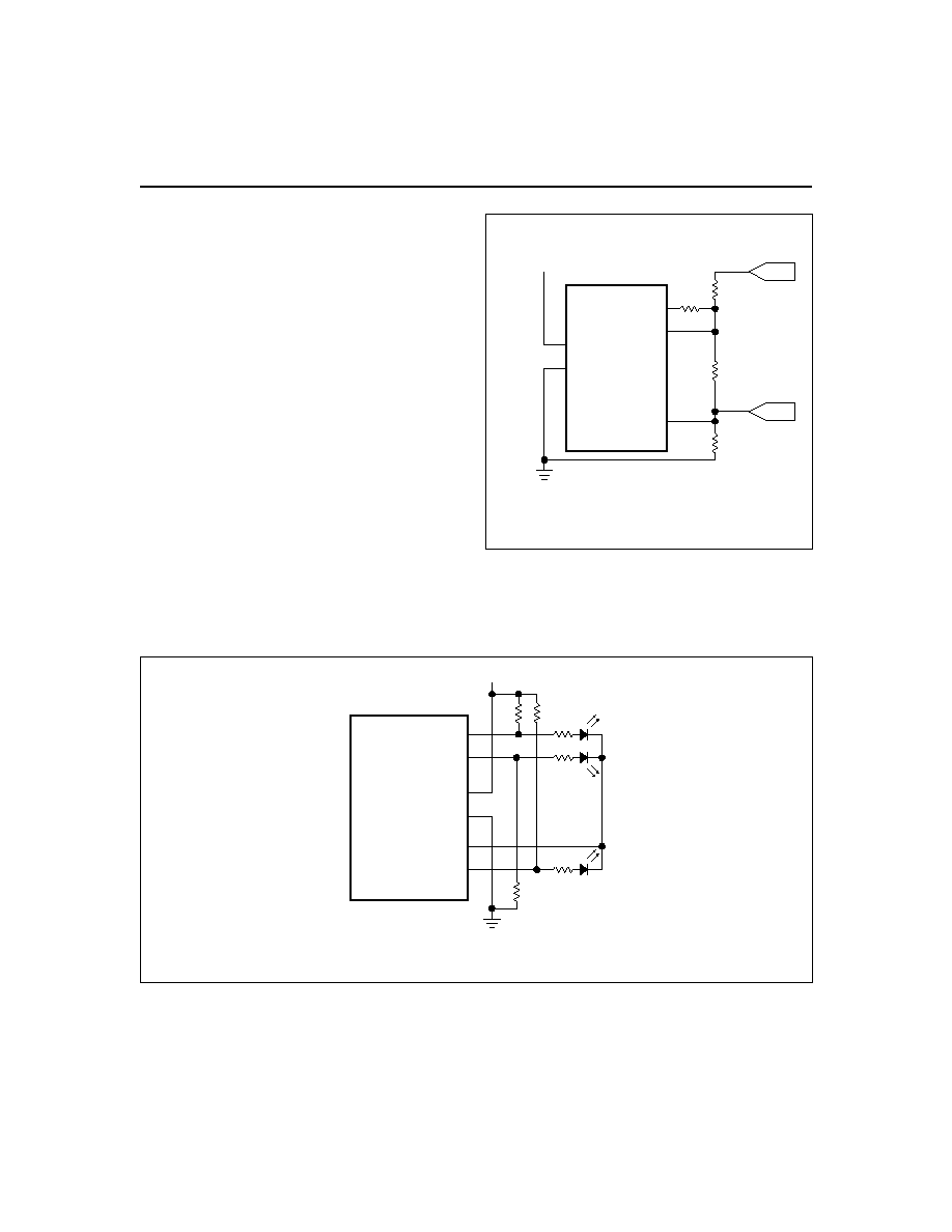
For example, Figure 5 shows the bq2031 configured for
the Pulsed Current algorithm and display mode 2.
Voltage and Current Monitoring
The bq2031 monitors battery pack voltage at the BAT
pin. A voltage divider between the positive and negative
terminals of the battery pack is used to present a scaled
battery pack voltage to the BAT pin and an appropriate
value for regulation of float (maintenance) voltage to the
FLOAT pin. The bq2031 also uses the voltage across a
sense resistor (R
SNS
) between the negative terminal
of the battery pack and ground to monitor current.
See Figure 6 for the configuration of this network.
6
bq2031
FG203103.eps
bq2031
LED1/TSEL
VCC
COM
LED3/QSEL
VCC
VSS
LED2/DSEL
16
15
13
12
11
10
10K
10K
1K
1K
1K
10K
VSS
Figure 5. Configuring Charging Algorithm and Display Mode
FG203102.eps
bq2031
BAT
VCC
SNS
VCC
VSS
FLOAT
2
3
13
12
7
RB3
BAT -
RSNS
VSS
BAT +
RB1
RB2
Figure 6. Configuring the Battery Divider

The resistor values are calculated from the following:
Equation 1
RB1
RB2
N
V
V
FLT
=
-
(
)
.
2 2
1
Equation 2
RB1
RB2
RB1
RB3
(
N
)
BLK
+
=
-
V
2 2
1
.
Equation 3
I
V
R
MAX
SNS
=
0 250
.
where:
n
N = Number of cells
n
V
FLT
= Desired float voltage
n
V
BLK
= Desired bulk charging voltage
n
I
MAX
= Desired maximum charge current
These parameters are typically specified by the battery
manufacturer. The total resistance presented across the
battery pack by RB1 + RB2 should be between 150k
and 1M
. The minimum value ensures that the divider
network does not drain the battery excessively when the
power source is disconnected. Exceeding the maximum
value increases the noise susceptibility of the BAT pin.
An empirical procedure for setting the values in the re-
sistor network is as follows:
1.
Set RB2 to 49.9 k
. (for 3 to 18 series cells)
2.
Determine RB1 from equation 1 given V
FLT
3.
Determine RB3 from equation 2 given V
BLK
4.
Calculate R
SNS
from equation 3 given I
MAX
Battery Insertion and Removal
The bq2031 uses V
BAT
to detect the presence or absence
of a battery. The bq2031 determines that a battery is
present when V
BAT
is between the High-Voltage Cutoff
(V
HCO
= 0.6 * V
CC
) and the Low-Voltage Cutoff (V
LCO
=
0.8V). When V
BAT
is outside this range, the bq2031 de-
termines that no battery is present and transitions to
the Fault state. Transitions into and out of the range
between V
LCO
and V
HCO
are treated as battery inser-
tions and removals, respectively. Besides being used to
detect battery insertion, the V
HCO
limit implicitly serves
as an over-voltage charge termination, because exceed-
ing this limit causes the bq2031 to believe that the bat-
tery has been removed.
The user must include a pull-up resistor from the posi-
tive terminal of the battery stack to VDC (and a diode to
prevent battery discharge through the power supply
when the supply is turned off) in order to detect battery
removal during periods of voltage regulation. Voltage
regulation occurs in pre-charge qualification test 1 prior
to all of the fast charge algorithms, and in phase 2 of the
Two-Step Voltage fast charge algorithm.
Temperature Monitoring
The bq2031 monitors temperature by examining the
voltage presented between the TS and SNS pins (V
TEMP
)
by a resistor network that includes a Negative Tempera-
ture Coefficient (NTC) thermistor. Resistance variations
around that value are interpreted as being proportional
to the battery temperature (see Figure 7).
The temperature thresholds used by the bq2031 and
their corresponding TS pin voltage are:
n
TCO--Temperature cutoff--Higher limit of the tem-
perature range in which charging is allowed. V
TCO
=
0.4 * V
CC
n
H T F -- H i g h - t e m p e r a t u r e f a u l t -- T h r e s h o l d t o
which temperature must drop after temperature
cutoff is exceeded before charging can begin again.
V
HTF
= 0.44 * V
CC
7
bq2031
FG203104.eps
VCC
VLTF = 0.6V
VHTF = 0.44V
VTCO = 0.4V
Hotter
VSS
TCO
HTF
LTF
Colder
Voltage
Temperature
Figure 7. Voltage Equivalent
of Temperature Thresholds

n
LTF--Low-temperature fault--Lower limit of the
temperature range in which charging is allowed. V
LTF
= 0.6 * V
CC
A resistor-divider network must be implemented that
presents the defined voltage levels to the TS pin at the
desired temperatures (see Figure 8).
The equations for determining RT1 and RT2 are:
Equation 4
0 6
0 250
1
.
(
.
)
(
)
(
)
=
-
+
+
V
V
V
RT1
RT2
R
RT2
R
CC
CC
LTF
LTF
Equation 5
0 44
1
1
.
(
)
(
)
=
+
+
RT1
RT2
R
RT2
R
HTF
HTF
where:
n
R
LTF
= thermistor resistance at LTF
n
R
HTF
= thermistor resistance at HTF
TCO is determined by the values of RT1 and RT2. 1%
resistors are recommended.
Disabling Temperature Sensing
Temperature sensing can be disabled by removing RT
and using a 100k
resistor for RT1 and RT2.
Temperature Compensation
The internal voltage reference used by the bq2031 for all
voltage threshold determinations is compensated for
temperature. The temperature coefficient is -3.9mV/∞C,
normalized to 25∞C. Voltage thresholds in the bq2031
vary by this proportion as ambient conditions change.
Fast-Charge Termination
Fast-charge termination criteria are programmed with
the fast charge algorithm per Table 1. Note that not all
criteria are applied in all algorithms.
Minimum Current
Fast charge terminates when the charging current drops
below a minimum current threshold programmed by the
value of IGSEL (see Table 3). This is used by the Two-
Step Voltage algorithm.
8
bq2031
FG203105.eps
bq2031
VCC
SNS
VCC
VSS
13
12
7
BAT -
RSNS
VSS
RT1
RT2
TS
8
RT
NTC
Thermistor
t
Figure 8. Configuring
Temperature Sensing
IGSEL
I
MIN
0
I
MAX
/10
1
I
MAX
/20
Z
I
MAX
/30
Table 3. I
MIN
Termination Thresholds

Second Difference (
2
V)
Second difference is a Unitrode proprietary algorithm
that accumulates the difference between successive sam-
ples of V
BAT
. The bq2031 takes a sample and makes a
termination decision at a frequency equal to 0.008 *
t
MTO
. Fast charge terminates when the accumulated dif-
ference is
-8mV. Second difference is used only in the
Two-Step Current algorithm, and is subject to a hold-off
period (see below).
Maximum Voltage
Fast charge terminates when V
CELL
V
BLK
. V
BLK
is set
per equation 2. Maximum voltage is used for fast charge
termination in the Two-Step Current and Pulsed Cur-
rent algorithms, and for transition from phase 1 to
phase 2 in the Two-Step Voltage algorithm. This crite-
rion is subject to a hold-off period.
Hold-off Periods
Maximum V and
2
V termination criteria are subject
to a hold-off period at the start of fast charge equal to
0.15 * t
MTO
. During this time, these termination criteria
are ignored.
Maximum Time-Out
Fast charge terminates if the programmed MTO time is
reached without some other termination shutting off
fast charge. MTO is programmed from 1 to 24 hours by
an R-C network on TMTO (see Figure 9) per the equa-
tion:
Equation 6
t
MTO
= 0.5 * R * C
where R is in k
, C is in µF, and t
MTO
is in hours. Typi-
cally, the maximum value for C of 0.1
µF is used.
Fast-charge termination by MTO is a Fault only in the
Pulsed Current algorithm; the bq2031 enters the Fault
state and waits for a new battery insertion, at which
time it begins a new charge cycle. In the Two-Step Volt-
age and Two-Step Current algorithms, the bq2031 tran-
sitions to the maintenance phase on MTO time-out.
The MTO timer starts at the beginning of fast charge. In
the Two-Step Voltage algorithm, it is cleared and re-
started when the bq2031 transitions from phase 1 (cur-
rent regulation) to phase 2 (voltage regulation). The
MTO timer is suspended (but not reset) during the out-
of-range temperature (Charge Pending) state.
Maintenance Charging
Three algorithms are used in maintenance charging:
n
Two-Step Voltage algorithm
n
Two-Step Current algorithm
n
Pulsed Current algorithm
Two-Step Voltage Algorithm
In the Two-Step Voltage algorithm, the bq2031 provides
charge maintenance by regulating charging voltage to
V
FLT
. Charge current during maintenance is limited to
I
COND
.
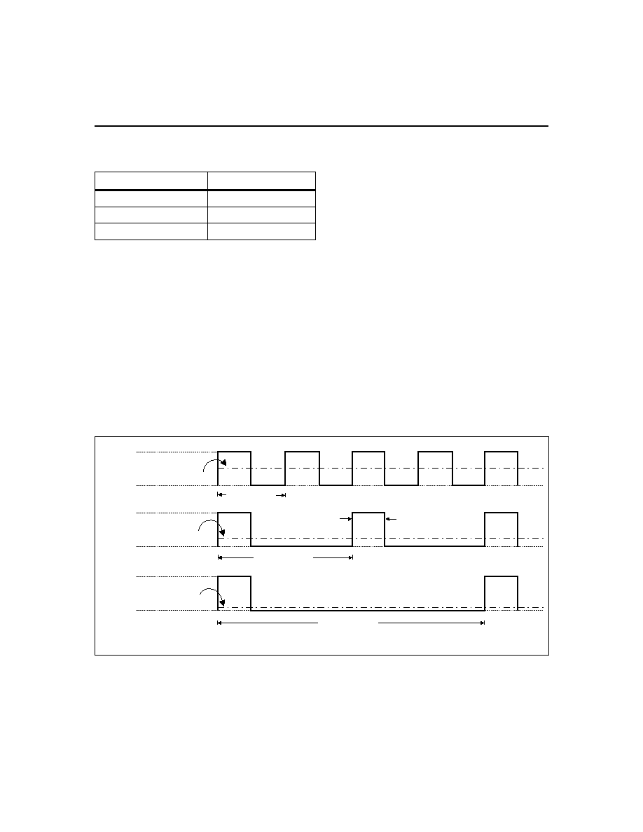
Two-Step Current Algorithm
Maintenance charging in the Two-Step Current Algo-
rithm is implemented by varying the period (T
P
) of a
fixed current (I
COND
= I
MAX
/5) and duration (0.2 sec-
onds) pulse to achieve the configured average mainte-
nance current value. See Figure 10.
Maintenance current can be calculated by:
Equation 7
Maintenance current
I
T
I
T
COND
P
MAX
P
=
=
(( . )
)
(( .
)
)
0 2
0 04
where T
P
is the period of the waveform in seconds.
Table 4 gives the values of P programmed by IGSEL.
9
bq2031
TM
FG203112.eps
VCC
VSS
bq2031
12
13
1
VSS
VCC
C
R
Figure 9. R-C Network for Setting MTO
Pulsed Current Algorithm
In the Pulsed Current algorithm, charging current is
turned off after the initial fast charge termination until
V
CELL
falls to V
FLT
. Full fast charge current (I
MAX
) is
then re-enabled to the battery until V
CELL
rises to V
BLK
.
This cycle repeats indefinitely.
Charge Regulation
The bq2031 controls charging through pulse-width modu-
lation of the MOD output pin, supporting both constant-
current and constant-voltage regulation. Charge current
is monitored by the voltage at the SNS pin, and charge
voltage by voltage at the BAT pin. These voltages are
compared to an internal temperature-compensated refer-
ence, and the MOD output modulated to maintain the de-
sired value.
Voltage at the SNS pin is determined by the value of re-
sistor R
SNS
, so nominal regulated current is set by:
Equation 8
I
MAX
= 0.250V/R
SNS
The switching frequency of the MOD output is deter-
mined by an external capacitor (CPWM) between the
pin TPWM and ground, per the following:
Equation 9
F
PWM
= 0.1/C
PWM
where C is in
µF and F is in kHz. A typical switching
rate is 100kHz, implying C
PWM
= 0.001
µF. MOD pulse
width is modulated between 0 and 80% of the switching
period.
To prevent oscillation in the voltage and current control
loops, frequency compensation networks (C or R-C) are
typically required on the VCOMP and ICOMP pins (respec-
tively) to add poles and zeros to the loop control equations.
A software program, "CNFG2031," is available to assist in
configuring these networks for buck type regulators. For
more detail on the control loops in buck topology, see the
application note, "Switch-Mode Power Conversion Using
the bq2031." For assistance with other power supply topolo-
gies, contact the factory.
10
bq2031
IGSEL
T
P
(sec.)
L
0.4
H
0.8
Z
1.6
Table 4. Fixed-Pulse Period by IGSEL
TD203101.eps
ICOND
ICOND
ICOND
0
0
0
IGSEL = L
Ave. Current
IGSEL = H
Ave. Current
IGSEL = Z
Ave. Current
TP = 1.6 Sec
TP = 0.8 Sec
TP = 0.4 Sec
0.2 Sec
Figure 10. Implementation of Fixed-Pulse Maintenance Charge

11
bq2031
Absolute Maximum Ratings
Symbol
Parameter
Minimum
Maximum
Unit
Notes
V
CC
V
CC
relative to V
SS
-0.3
+7.0
V
V
T
DC voltage applied on any pin ex-
cluding V
CC
relative to V
SS
-0.3
+7.0
V
T
OPR
Operating ambient temperature
-20
+70
∞C
Commercial
T
STG
Storage temperature
-55
+125
∞C
T
SOLDER
Soldering temperature
-
+260
∞C
10 s. max.
T
BIAS
Temperature under bias
-40
+85
∞C
Note:
Permanent device damage may occur if Absolute Maximum Ratings are exceeded. Functional opera-
tion should be limited to the Recommended DC Operating Conditions detailed in this data sheet. Expo-
sure to conditions beyond the operational limits for extended periods of time may affect device reliability.
DC Thresholds
(TA = TOPR; VCC = 5V
±10%)
Symbol
Parameter
Rating
Unit
Tolerance
Notes
V
REF
Internal reference voltage
2.20
V
1%
T
A
= 25∞C
Temperature coefficient
-3.9
mV/∞C
10%
V
LTF
TS maximum threshold
0.6 * V
CC
V
±0.03V
Low-temperature fault
V
HTF
TS hysteresis threshold
0.44 * V
CC
V
±0.03V
High-temperature fault
V
TCO
TS minimum threshold
0.4 * V
CC
V
±0.03V
Temperature cutoff
V
HCO
High cutoff voltage
0.60 * V
CC
V
±0.03V
V
MIN
Under-voltage threshold at BAT
0.34 * V
CC
V
±0.03V
V
LCO
Low cutoff voltage
0.8
V
±0.03V
V
SNS
Current sense at SNS
0.250
V
10%
I
MAX
0.05
V
10%
I
COND

12
bq2031
Recommended DC Operating Conditions
(TA = TOPR)
Symbol
Parameter
Minimum
Typical
Maximum
Unit
Notes
V
CC
Supply voltage
4.5
5.0
5.5
V
V
TEMP
TS voltage potential
0
-
V
CC
V
V
TS
- V
SNS
V
CELL
Battery voltage potential
0
-
V
CC
V
V
BAT
- V
SNS
I
CC
Supply current
-
2
4
mA
Outputs unloaded
I
IZ
DSEL tri-state open detection
-2
-
2
µA
Note 2
IGSEL tri-state open detection
-2
2
µA
V
IH
Logic input high
V
CC
-1.0
-
-
V
QSEL,TSEL
V
CC
-0.3
-
-
V
DSEL, IGSEL
V
IL
Logic input low
-
-
V
SS
+1.0
V
QSEL,TSEL
-
-
V
SS
+0.3
V
DSEL, IGSEL
V
OH
LED
1
, LED
2
, LED
3
, output high
V
CC
-0.8
-
-
V
I
OH
10mA
MOD output high
V
CC
-0.8
-
-
V
I
OH
10mA
V
OL
LED
1
, LED
2
, LED
3
, output low
-
-
V
SS
+0.8V
V
I
OL
10mA
MOD output low
-
-
V
SS
+0.8V
V
I
OL
10mA
FLOAT output low
-
-
V
SS
+0.8V
V
I
OL
5mA, Note 3
COM output low
-
-
V
SS+
0.5
V
I
OL
30mA
I
OH
LED
1
, LED
2
, LED
3
, source
-10
-
-
mA
V
OH
=V
CC
-0.5V
MOD source
-5.0
-
-
mA
V
OH
=V
CC
-0.5V
I
OL
LED
1
, LED
2
, LED
3
, sink
10
-
-
mA
V
OL
= V
SS
+0.5V
MOD sink
5
-
-
mA
V
OL
= V
SS
+0.8V
FLOAT sink
5
-
-
mA
V
OL
= V
SS
+0.8V, Note 3
COM sink
30
-
-
mA
V
OL
= V
SS
+0.5V
I
IL
DSEL logic input low source
-
-
+30
µA
V = V
SS
to V
SS
+ 0.3V, Note 2
IGSEL logic input low source
-
-
+70
µA
V = V
SS
to V
SS
+ 0.3V
I
IH
DSEL logic input high source
-30
-
-
µA
V = V
CC
- 0.3V to V
CC
IGSEL logic input high source
-70
-
-
µA
V = V
CC
- 0.3V to V
CC
I
L
Input leakage
-
-
±1
µA
QSEL, TSEL, Note 2
Notes:
1.
All voltages relative to V
SS
except where noted.
2.
Conditions during initialization after V
CC
applied.
3.
SNS = 0V.

13
bq2031
Impedance
Symbol
Parameter
Minimum
Typical
Maximum
Unit
Notes
R
BATZ
BAT pin input impedance
50
-
-
M
R
SNSZ
SNS pin input impedance
50
-
-
M
R
TSZ
TS pin input impedance
50
-
-
M
R
PROG1
Soft-programmed pull-up or pull-down
resistor value (for programming)
-
-
10
k
DSEL, TSEL, and
QSEL
R
PROG2
Pull-up or pull-down resistor value
-
-
3
k
IGSEL
R
MTO
Charge timer resistor
20
-
480
k
Timing
(TA = TOPR; VCC = 5V
±10%)
Symbol
Parameter
Minimum
Typical
Maximum
Unit
Notes
t
MTO
Charge time-out range
1
-
24
hours
See Figure 9
t
QT1
Pre-charge qual test 1 time-out period
-
0.02t
MTO
-
-
t
QT2
Pre-charge qual test 2 time-out period
-
0.16t
MTO
-
-
t
DV
2
V termination sample frequency
-
0.008t
MTO
-
-
t
H01
Pre-charge qual test 2 hold-off period
-
0.002t
MTO
-
-
t
H02
Bulk charge hold-off period
-
0.015t
MTO
-
-
F
PWM
PWM regulator frequency range
-
100
kHz
See Equation 9
Capacitance
Symbol
Parameter
Minimum
Typical
Maximum
Unit
C
MTO
Charge timer capacitor
-
0.1
0.1
µF
C
PWM
PWM R-C capacitance
-
0.001
-
µF

14
bq2031
16-Pin SOIC Narrow (SN)
A
A1
.004
C
B
e
D
E
H
L
16-Pin SN (0.150" SOIC)
Dimension
Inches
Millimeters
Min.
Max.
Min.
Max.
A
0.060
0.070
1.52
1.78
A1
0.004
0.010
0.10
0.25
B
0.013
0.020
0.33
0.51
C
0.007
0.010
0.18
0.25
D
0.385
0.400
9.78
10.16
E
0.150
0.160
3.81
4.06
e
0.045
0.055
1.14
1.40
H
0.225
0.245
5.72
6.22
L
0.015
0.035
0.38
0.89
16-Pin PN (0.300" DIP)
Dimension
Inches
Millimeters
Min.
Max.
Min.
Max.
A
0.160
0.180
4.06
4.57
A1
0.015
0.040
0.38
1.02
B
0.015
0.022
0.38
0.56
B1
0.055
0.065
1.40
1.65
C
0.008
0.013
0.20
0.33
D
0.740
0.770
18.80
19.56
E
0.300
0.325
7.62
8.26
E1
0.230
0.280
5.84
7.11
e
0.300
0.370
7.62
9.40
G
0.090
0.110
2.29
2.79
L
0.115
0.150
2.92
3.81
S
0.020
0.040
0.51
1.02
16-Pin DIP Narrow (PN)
15
bq2031
Change No.
Page No.
Description
Nature of Change
1
Descriptions
Clarified and consolidated
1
Renamed
Dual-Level Constant Current Mode to Two-Step Current Mode
V
MCV
to V
HCO
V
INT
to V
LCO
t
UV1
to t
QT1
t
UV2
to t
QT2
1
Consolidation
Tables 1 and 2
1
Added figures
Start-up states
Temperature sense input voltage thresholds
Pulsed maintenance current implementation
1
Updated figures
Figures 1 through 6
1
Added equations
Thermistor divider network configuration equations
1
Raised condition
MOD V
OL
and V
OH
parameters from
5mA to 10µA
1
Corrected Conditions
VSNS rating from V
MAX
and V
MIN
to I
MAX
and I
MIN
1
Added table
Capacitance table for C
MTO
and C
PWM
2
6
Changed values in
Figure 5
Was 51K; is now 10K
3
7, 10
Changed values
in Equations 3 and 8
Was: I
MAX
= 0.275V/R
SNS
; is now I
MAX
= 0.250V/R
SNS
3
8
Changed values
in Equation 4
Was: (V
CC
- 0.275); is now (V
CC
- 0.250V)
3
11
Changed rating value
for V
SNS
in DC
Thresholds table
Was 0.275; is now 0.250
4
11
T
OPR
Deleted industrial temperature range.
Notes:
Change 1 = Dec. 1995 B changes from June 1995 A.
Change 2 = Sept. 1996 C changes from Dec. 1995 B.
Change 3 = April 1997 D changes from Sept. 1996 C.
Change 4 = June 1999 E changes from April 1997 D.
Data Sheet Revision History
bq2031
Package Option:
PN
= 16-pin plastic DIP
SN
= 16-pin narrow SOIC
Device:
bq2031 Lead Acid Charge IC
Ordering Information

16
IMPORTANT NOTICE
Texas Instruments and its subsidiaries (TI) reserve the right to make changes to their products or to discontinue any
product or service without notice, and advise customers to obtain the latest version of relevant information to verify,
before placing orders, that information being relied on is current and complete. All products are sold subject to the
terms and conditions of sale supplied at the time of order acknowledgement, including those pertaining to warranty,
patent infringement, and limitation of liability.
TI warrants performance of its semiconductor products to the specifications applicable at the time of sale in accor-
dance with TI's standard warranty. Testing and other quality control techniques are utilized to the extent TI deems
necessary to support this warranty. Specific testing of all parameters of each device is not necessarily performed, ex-
cept those mandated by government requirements.
CERTAIN APPLICATIONS USING SEMICONDUCTOR PRODUCTS MAY INVOLVE POTENTIAL RISKS OF DEATH,
PERSONAL INJURY, OR SEVERE PROPERTY OR ENVIRONMENTAL DAMAGE ("CRITICAL APPLICATIONS"). TI
SEMICONDUCTOR PRODUCTS ARE NOT DESIGNED, AUTHORIZED, OR WARRANTED TO BE SUITABLE FOR
USE IN LIFE-SUPPORT DEVICES OR SYSTEMS OR OTHER CRITICAL APPLICATIONS. INCLUSION OF TI
PRODUCTS IN SUCH APPLICATIONS IS UNDERSTOOD TO BE FULLY AT THE CUSTOMER'S RISK.
In order to minimize risks associated with the customer's applications, adequate design and operating safeguards
must be provided by the customer to minimize inherent or procedural hazards.
TI assumes no liability for applications assistance or customer product design. TI does not warrant or represent that
any license, either express or implied, is granted under any patent right, copyright, mask work right, or other intellec-
tual property right of TI covering or relating to any combination, machine, or process in which such semiconductor
products or services might be or are used. TI's publication of information regarding any third party's products or ser-
vices does not constitute TI's approval, warranty or endorsement thereof.
Copyright © 1999, Texas Instruments Incorporated