 | ÐлекÑÑоннÑй компоненÑ: BQ2050SNN | СкаÑаÑÑ:  PDF PDF  ZIP ZIP |
Äîêóìåíòàöèÿ è îïèñàíèÿ www.docs.chipfind.ru

1
Features
Conservative and repeatable
measurement of available capac-
ity in Lithium Ion rechargeable
batteries
Designed for battery pack inte-
gration
-
120
µA typical operating
current
-
Small size enables imple-
mentations in as little as
1
2
square inch of PCB
Integrate within a system or as a
stand-alone device
-
Display capacity via single-
wire serial communication
port or direct drive of LEDs
Measurements compensated for
current and temperature
Self-discharge compensation us-
ing internal temperature sensor
16-pin narrow SOIC
General Description
The bq2050 Lithium Ion Power
GaugeTM IC is intended for battery-
pack or in-system installation to
maintain an accurate record of
available battery capacity. The IC
monitors a voltage drop across a
sense resistor connected in series
between the negative battery termi-
n a l a n d g r o u n d t o d e t e r m i n e
charge and discharge activity of
the battery. Compensations for bat-
tery temperature and rate of charge
or discharge are applied to the
charge, discharge, and self-discharge
calculations to provide available ca-
pacity information across a wide
range of operating conditions. Bat-
tery capacity is automatically recali-
brated, or "learned," in the course of
a discharge cycle from full to empty.
Nominal available capacity may be
directly indicated using a five-
segment LED display. These seg-
ments are used to graphically indi-
cate available capacity. The bq2050
supports a simple single-line bidi-
rectional serial link to an external
processor (common ground). The
bq2050 outputs battery information
in response to external commands
over the serial link.
The bq2050 may operate directly
from one cell (V
BAT
> 3V). With the
REF output and an external transis-
tor, a simple, inexpensive regulator
can be built for systems with more
than one series cell.
Internal registers include available
capacity, temperature, scaled avail-
able energy, battery ID, battery
status, and programming pin set-
tings. To support subassembly test-
ing, the outputs may also be con-
trolled. The external processor may
also overwrite some of the bq2050
power gauge data registers.
LCOM
LED common output
SEG
1
/PROG
1
LED segment 1/
program 1 input
SEG
2
/PROG
2
LED segment 2/
program 2 input
SEG
3
/PROG
3
LED segment 3/
program 3 input
SEG
4
/PROG
4
LED segment 4/
program 4 input
SEG
5
/PROG
5
LED segment 5/
program 5 input
PROG
6
Program 6 input
1
PN205001.eps
16-Pin Narrow SOIC
2
3
4
5
6
7
8
16
15
14
13
12
11
10
9
VCC
REF
N/C
DQ
RBI
SB
DISP
SR
LCOM
SEG1/PROG1
SEG2/PROG2
SEG3/PROG3
SEG4/PROG4
SEG5/PROG5
PROG6
VSS
REF
Voltage reference output
N/C
No connect
DQ
Serial communications
input/output
RBI
Register backup input
SB
Battery sense input
DISP
Display control input
SR
Sense resistor input
V
CC
3.06.5V
V
SS
System ground
Pin Connections
Pin Names
bq2050
9/96 C
Lithium Ion Power GaugeTM IC

Pin Descriptions
LCOM
LED common output
Open-drain output switches V
CC
to source
current for the LEDs. The switch is off dur-
ing initialization to allow reading of the soft
pull-up
or
pull-down
program
resistors.
LCOM is also high impedance when the dis-
play is off.
SEG
1
SEG
5
LED display segment outputs (dual func-
tion with PROG
1
PROG
6
)
Each output may activate an LED to sink
the current sourced from LCOM.
PROG
1
PROG
2
Programmed full count selection inputs
(dual function with SEG
1
SEG
2
)
These three-level input pins define the pro-
grammed full count (PFC) thresholds de-
scribed in Table 2.
PROG
3
PROG
4
Power gauge rate selection inputs (dual
function with SEG
3
SEG
4
)
These three-level input pins define the scale
factor described in Table 2.
PROG
5
Self-discharge rate selection (dual func-
tion with SEG
5
)
This
three-level
input
pin
defines
the
selfdischarge and battery compensation fac-
tors as shown in Table 1.
PROG
6
Capacity initialization selection
This three-level pin defines the battery state
of charge at reset as shown in Table 1.
N/C
No connect
SR
Sense resistor input
The voltage drop (V
SR
) across the sense re-
sistor R
S
is monitored and integrated over
time to interpret charge and discharge activ-
ity. The SR input is tied between the nega-
tive terminal of the battery and the sense re-
sistor. V
SR
< V
SS
indicates discharge, and V
SR
> V
SS
indicates charge. The effective voltage
drop, V
SRO
, as seen by the bq2050 is V
SR
+
V
OS
.
DISP
Display control input
DISP high disables the LED display. DISP
tied to V
CC
allows PROG
X
to connect directly
to V
CC
or V
SS
instead of through a pull-up or
pull-down resistor. DISP floating allows the
LED display to be active during charge.
DISP low activates the display. See Table 1.
SB
Secondary battery input
This input monitors the battery cell voltage
potential through a high-impedance resis-
tive divider network for end-of-discharge
voltage (EDV) thresholds, and battery re-
moved.
RBI
Register backup input
This pin is used to provide backup potential to
the bq2050 registers during periods when
V
CC
3V. A storage capacitor or a battery
can be connected to RBI.
DQ
Serial I/O pin
This is an open-drain bidirectional pin.
REF
Voltage reference output for regulator
REF provides a voltage reference output for
an optional micro-regulator.
V
CC
Supply voltage input
V
SS
Ground
2
bq2050
Functional Description
General Operation
The bq2050 determines battery capacity by monitor-
ing the amount of current input to or removed from a
rechargeable battery.
The bq2050 measures dis-
charge and charge currents, measures battery volt-
age, estimates self-discharge, monitors the battery
for low battery voltage thresholds, and compensates
for temperature and charge/discharge rates. The cur-
rent measurement is made by monitoring the voltage
across a small-value series sense resistor between the
negative battery terminal and ground. The estimate of
scaled available energy is made using the remaining
average battery voltage during the discharge cycle
and the remaining nominal available charge. The
scaled available energy measurement is corrected for
the environmental and operating conditions.
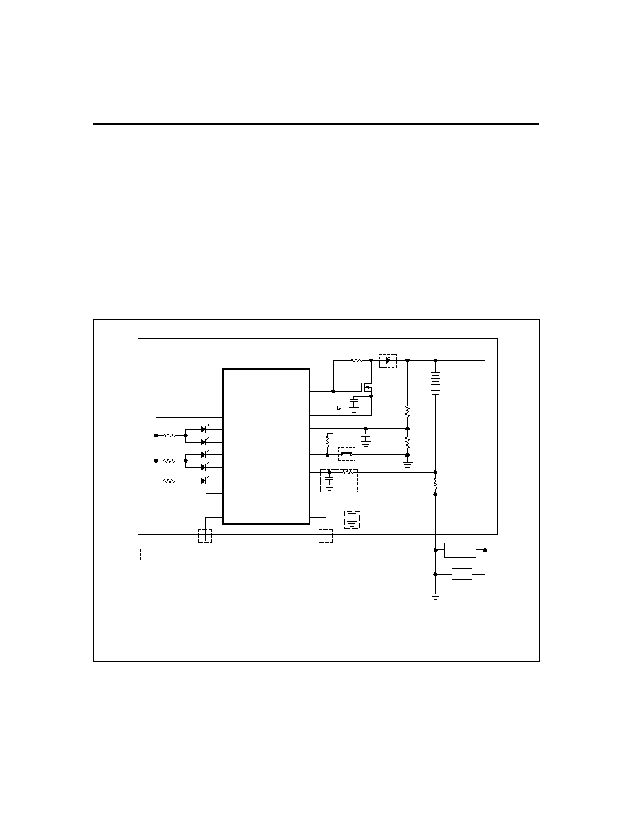
Figure 1 shows a typical battery pack application of the
bq2050 using the LED display capability as a charge-
state indicator. The bq2050 is configured to display ca-
pacity in relative display mode.
The relative display
mode uses the last measured discharge capacity of the
battery as the battery "full" reference. A push-button
display feature is available for momentarily enabling
the LED display.
The bq2050 monitors the charge and discharge currents
as a voltage across a sense resistor (see R
S
in Figure 1).
A filter between the negative battery terminal and the
SR pin may be required if the rate of change of the bat-
tery current is too great.
3
bq2050
FG205001.eps
PROG6
SEG5/PROG5
SEG4/PROG4
SEG3/PROG3
SEG2/PROG2
SEG1/PROG1
SR
DISP
SB
VCC
REF
bq2050
Power Gauge IC
LCOM
VSS
RBI
DQ
VCC
C1
0.1 F
Q1
ZVNL110A
R1
RS
RB1
RB2
Load
Charger
Indicates optional.
Directly connect to VCC across 1 cell (VBAT > 3V).
Otherwise, R1, C1, and Q1 are needed for regulation of > 1 cell.
Programming resistors (6 max.) and ESD-protection diodes are not shown.
R-C on SR may be required, application-specific.
A series Zener may be used to limit discharge current at low voltages
in designs using 3 or more cells.
VCC
C2
1M
PSTAT
Figure 1. Battery Pack Application Diagram--LED Display

Voltage Thresholds
In conjunction with monitoring V
SR
for charge/discharge
currents, the bq2050 monitors the battery potential
through the SB pin. The voltage is determined through
a resistor-divider network per the following equation:
RB1
RB2
2N
=
- 1
where N is the number of cells, RB1 is connected to the
positive battery terminal, and RB2 is connected to the
negative battery terminal. The single-cell battery volt-
age is monitored for the end-of-discharge voltage (EDV).
EDV threshold levels are used to determine when the
battery has reached an "empty" state.
Two EDV thresholds for the bq2050 are programmable
with the default values fixed at:
EDV1 (early warning) = 1.52V
EDVF (empty) = 1.47V
If V
SB
is below either of the two EDV thresholds, the as-
sociated flag is latched and remains latched, independ-
ent of V
SB
, until the next valid charge. The V
SB
value is
also available over the serial port.
During discharge and charge, the bq2050 monitors V
SR
for various thresholds used to compensate the charge
and discharge rates. Refer to the count compensation
section for details. EDV monitoring is disabled if the
discharge rate is greater than 2C (typical) and resumes
1
2
second after the rate falls below 2C.
RBI Input
The RBI input pin is intended to be used with a storage ca-
pacitor or external supply to provide backup potential to the
internal bq2050 registers when V
CC
drops below 3.0V. V
CC
is output on RBI when V
CC
is above 3.0V. A diode is re-
quired to isolate the external supply.
Reset
The bq2050 can be reset either by removing V
CC
and
grounding the RBI pin for 15 seconds or by writing 0x80
to register 0x39.
Temperature
The bq2050 internally determines the temperature in
10°C steps centered from approximately -35°C to +85°C.
The temperature steps are used to adapt charge and dis-
charge rate compensations, self-discharge counting, and
available charge display translation. The temperature
range is available over the serial port in 10°C incre-
ments as shown in the following table:
Layout Considerations
The bq2050 measures the voltage differential between
the SR and V
SS
pins. V
OS
(the offset voltage at the SR
pin) is greatly affected by PC board layout. For optimal
results, the PC board layout should follow the strict rule
of a single-point ground return. Sharing high-current
ground with small signal ground causes undesirable
noise on the small signal nodes. Additionally:
n
The capacitors (C1 and C2) should be placed as
close as possible to the V
CC
and SB pins,
respectively, and their paths to V
SS
should be as
short as possible. A high-quality ceramic capacitor
of 0.1
µf is recommended for V
CC
.
n
The sense resistor capacitor should be placed as close
as possible to the SR pin.
n
The sense resistor (R
S
) should be as close as possible to
the bq2050.
4
bq2050
TMP (hex)
Temperature Range
0x
< -30°C
1x
-30°C to -20°C
2x
-20°C to -10°C
3x
-10°C to 0°C
4x
0°C to 10°C
5x
10°C to 20°C
6x
20°C to 30°C
7x
30°C to 40°C
8x
40°C to 50°C
9x
50°C to 60°C
Ax
60°C to 70°C
Bx
70°C to 80°C
Cx
> 80°C
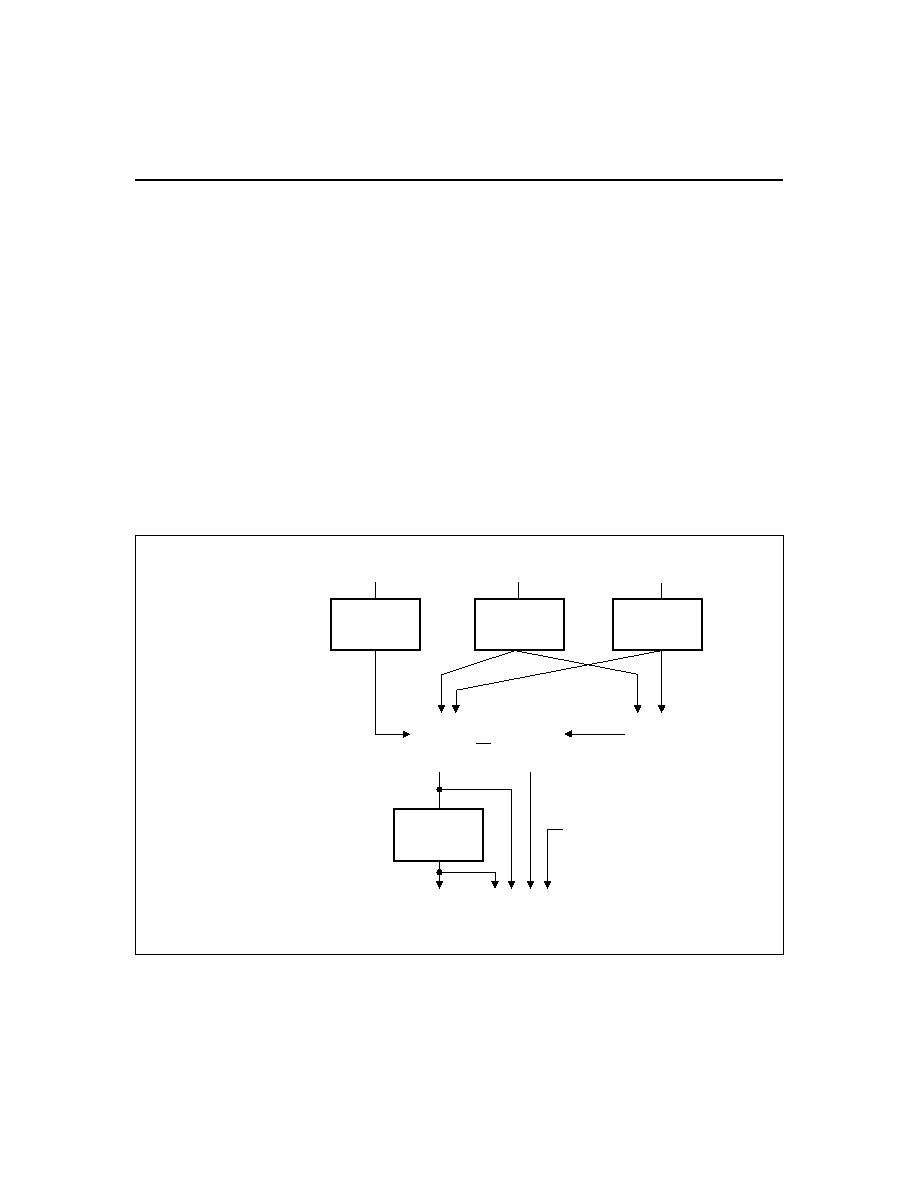
Gas Gauge Operation
The operational overview diagram in Figure 2 illustrates
the operation of the bq2050. The bq2050 accumulates a
measure of charge and discharge currents, as well as an
estimation of self-discharge. Charge and discharge cur-
rents are temperature and rate compensated, whereas
self-discharge is only temperature compensated.
The main counter, Nominal Available Capacity (NAC),
represents the available battery capacity at any given
time.
Battery charging increments the NAC register,
while battery discharging and self-discharge decrement
the NAC register and increment the DCR (Discharge
Count Register).
The Discharge Count Register (DCR) is used to update
the Last Measured Discharge (LMD) register only if a
complete battery discharge from full to empty occurs
without any partial battery charges.
Therefore, the
bq2050 adapts its capacity determination based on the
actual conditions of discharge.
The battery's initial capacity is equal to the Pro-
grammed Full Count (PFC) shown in Table 2. Until
LMD is updated, NAC counts up to but not beyond this
threshold during subsequent charges. This approach al-
lows the gas gauge to be charger-independent and com-
patible with any type of charge regime.
1.
Last Measured Discharge (LMD) or learned
battery capacity:
LMD is the last measured discharge capacity of the
battery. On initialization (application of V
CC
or bat-
tery replacement), LMD = PFC. During subsequent
discharges, the LMD is updated with the latest
measured capacity in the Discharge Count Register
(DCR) representing a discharge from full to below
EDV1. A qualified discharge is necessary for a capac-
ity transfer from the DCR to the LMD register. The
LMD also serves as the 100% reference threshold
used by the relative display mode.
5
bq2050
FG205002.eps
Rate and
Temperature
Compensation
Temperature
Compensation
Charge
Current
Discharge
Current
Self-Discharge
Timer
Temperature
Translation
Nominal
Available
Charge
(NAC)
Last
Measured
Discharged
(LMD)
Discharge
Count
Register
(DCR)
<
Qualified
Transfer
+
Rate and
Temperature
Compensation
Rate and
Temperature
Compensation
Temperature Step,
Other Data
+
-
-
+
Inputs
Main Counters
and Capacity
Reference (LMD)
Outputs
Serial
Port
Compensated
Available Charge
LED Display, etc.
Figure 2. Operational Overview