 | ÐлекÑÑоннÑй компоненÑ: BQ2092SN | СкаÑаÑÑ:  PDF PDF  ZIP ZIP |
Äîêóìåíòàöèÿ è îïèñàíèÿ www.docs.chipfind.ru

Features
Provides accurate measure-
ment of available charge in
NiCd, NiMH, and Li-Ion re-
chargeable batteries
Supports SBData charge con-
trol commands for Li-Ion,
NiMH, and NiCd chemistries
Designed for battery pack inte-
gration
-
120
µA typical operating
current
-
Small size enables
implementations in as little as
3
4
square inch of PCB
Two-wire SMBus-like interface
Measurements compensated for
current and temperature
Programmable self-discharge
and charge compensation
16-pin narrow SOIC
General Description
The bq2092 Gas Gauge IC With
SMBus-Like Interface is intended
for battery-pack or in-system instal-
lation to maintain an accurate
record of available battery charge.
The bq2092 directly supports capac-
ity monitoring for NiCd, NiMH, and
Li-Ion battery chemistries.
The bq2092 uses the SMBus proto-
col that supports many of the Smart
Battery Data (SBData) commands.
The bq2092 also supports SBData
charge control.
Battery state-of-
charge, capacity remaining, remain-
ing time and chemistry are available
over the serial link. Battery-charge
state can be directly indicated using
a four-segment LED display to
graphically depict battery full-to-
empty in 25% increments.
The bq2092 estimates battery self-
discharge based on an internal
timer and temperature sensor and
user-programmable rate informa-
tion stored in external EEPROM.
The bq2092 also automatically
recalibrates or "learns" battery
capacity in the full course of a
discharge cycle from full to empty.
The bq2092 may operate directly
from three nickel chemistry cells.
With the REF output and an exter-
nal transistor, a simple, inexpensive
regulator can be built to provide V
CC
for other battery cell configurations.
An external EEPROM is used to
program initial values into the
bq2092 and is necessary for proper
operation.
1
bq2092
Gas Gauge IC with SMBus-Like Interface
V
CC
3.05.5V
SCL
Serial memory
clock
SDA
Serial memory
data
SEG
1
LED segment 1
SEG
2
LED segment 2
SEG
3
LED segment 3
SEG
4
LED segment 4
V
SS
System ground
1
PN209101.eps
16-Pin Narrow SOIC
2
3
4
5
6
7
8
16
15
14
13
12
11
10
9
VOUT
REF
SCC
SCD
NC
SB
DISP
SR
VCC
SCL
SDA
SEG1
SEG2
SEG3
SEG4
VSS
SR
Sense resistor input
DISP
Display control input
SB
Battery sense input
SCD
Serial communication
data input/output
SCC
Serial communication
clock
REF
Voltage reference
output
V
OUT
EEPROM supply
output
6/99 C
Pin Connections
Pin Names

Pin Descriptions
V
CC
Supply voltage input
SCL
Serial memory clock
This output is used to clock the data
transfer between the bq2092 and the ex-
ternal nonvolatile configuration memory.
SDA
Serial memory data and address
This bi-directional pin is used to trans-
fer address and data to and from the
bq2092 and the external configuration
memory.
SEG
1
SEG
4
LED display segment outputs
Each output may activate an external LED
to sink the current sourced from V
CC
.
V
SS
Ground
SR
Sense resistor input
The voltage drop (V
SR
) across pins SR and
V
SS
is monitored and integrated over time
to interpret charge and discharge activity.
The SR input is connected to the sense re-
sistor and the negative terminal of the
battery. V
SR
< V
SS
indicates discharge, and
V
SR
> V
SS
indicates charge. The effective
voltage drop, V
SRO
, as seen by the bq2092
is V
SR
+ V
OS
(see Table 3).
DISP
Display control input
DISP high disables the LED display. DISP
floating allows the LED display to be active
during charge if the rate is greater than
100mA. DISP low activates the display for 4
seconds.
SB
Secondary battery input
This input monitors the cell pack voltage as
a single-cell potential through a high-
impedance resistor divider network.
The
cell pack voltage is reported in the SBD
register function Voltage (0x09) and is com-
pared to end-of-discharge voltage and
charging voltage parameters.
NC
No connect
SCD
Serial communication data
This open-drain bidirectional pin is used to
transfer address and data to and from the
bq2092.
SCC
Serial communication clock
This open-drain bidirectional pin is used to
clock the data transfer to and from the
bq2092.
REF
Reference output for regulator
REF provides a reference output for an op-
tional micro-regulator.
V
OUT
Supply output
This output supplies power to the exter-
nal EEPROM configuration memory.
2
bq2092
Functional Description
General Operation
The bq2092 determines battery capacity by monitoring
the amount of charge input to or removed from a
rechargeable battery. The bq2092 measures discharge
and charge currents, estimates self-discharge, and
monitors the battery for low-battery voltage thresh-
olds. The charge measurement is made by monitoring
the voltage across a small-value series sense resistor
between the battery's negative terminal and ground.
The available battery charge is determined by moni-
toring this voltage over time and correcting the meas-
urement for the environmental and operating condi-
tions.
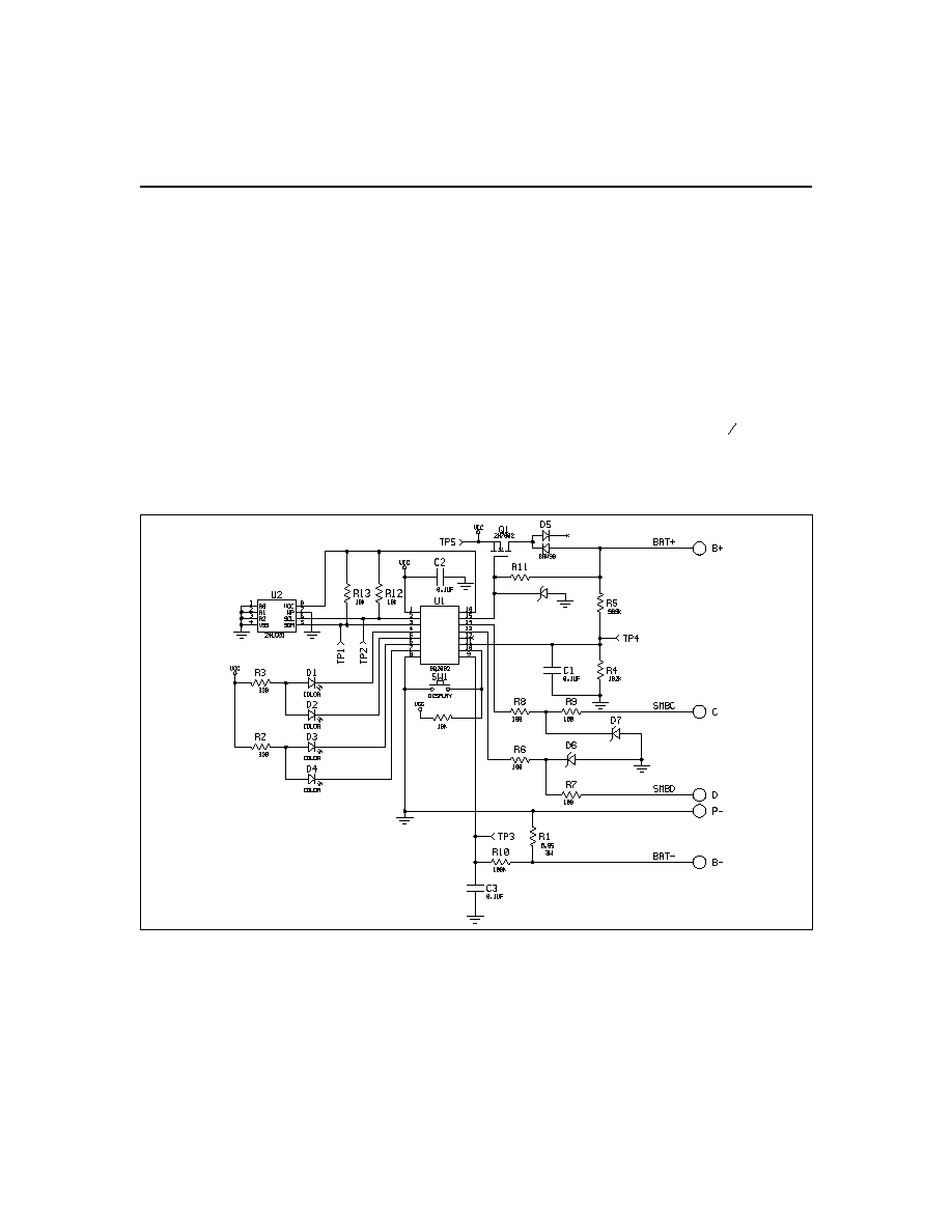
Figure 1 shows a typical battery pack application of the
bq2092 using the LED capacity display, the serial port,
and an external EEPROM for battery pack program-
ming information. The bq2092 must be configured and
calibrated for the battery-specific information to ensure
proper operation. Table 1 outlines the externally
programmable functions available in the bq2092. Refer
to the Programming the bq2092 section for further
details.
An internal temperature sensor eliminates the need
for an external thermistor--reducing cost and compo-
nents.
An internal, temperature-compensated time-
base eliminates the need for an external resonator,
further reducing cost and components.
The entire
circuit in Figure 1 can occupy less than
3
4
square inch
of board space.
3
bq2092
VCC
SCL
SDA
SEG1
SEG2
SEG3
SEG4
VOUT
REF
SCC
SCD
NC
SB
DISP
SR
BZX84C5V6
BZX84C5V6
2192L.eps
Figure 1. Battery Pack Application Diagram--LED Display

4
Parameter Name
Address
Length
Units
Design capacity
0x00/0x01
16 bits: low byte, high byte
mAh
Initial battery voltage
0x02/0x03
16 bits: low byte, high byte
mV
Fast charging current
0x04/0x05
16 bits: low byte, high byte
mA
Charging voltage
0x06/0x07
16 bit: low byte, high byte
mV
Remaining capacity alarm
0x08/0x09
16 bits: low byte, high byte
mAh
FLAGS1
0x0a
8 bits
N/A
FLAGS2
0x0b
8 bits
N/A
Current measurement gain
0x0c/0x0d
16 bits: low byte, high byte
N/A
EDV
1
0x0e/0x0f
16 bits: low byte, high byte
mV
EDV
F
0x10/0x11
16 bits: low byte, high byte
mV
Temperature offset
0x12
8 bits
0.1°K
Maximum charge temperature/
T/t
0x13
8 bits
N/A
Self-discharge rate
0x14
8 bits
N/A
Digital filter
0x15
8 bits
N/A
Current integration gain
0x16/0x17
16 bits: low byte, high byte
N/A
Full charge percentage
0x18
8 bits
N/A
Charge compensation
0x19
8 bits
N/A
Battery voltage offset
0x1a
8 bits
mV
Battery voltage gain
0x1b/0x1c
16 bits: high byte, low byte
N/A
Serial number
0x1d/0x1e
16 bits: low byte, high byte
N/A
Hold-off timer
0x1f
8 bits
N/A
Cycle count
0x20/0x21
16 bits: low byte, high byte
N/A
Maintenance charge current
0x22/0x23
16 bits: low byte, high byte
mA
Reserved
0x24/0x31
Design voltage
0x32/0x33
16 bits: low byte, high byte
mV
Specification information
0x34/0x35
16 bits: low byte, high byte
N/A
Manufacturer date
0x36/0x37
16 bits: low byte, high byte
N/A
Reserved
0x38/0x3f
Manufacturer name
0x40/0x4f
8 + 120 bits
N/A
Device name
0x50/0x5f
8 + 120 bits
N/A
Chemistry
0x60/0x6f
8 + 120 bits
N/A
Manufacturer data
0x70/0x7f
8 +120 bits
N/A
Table 1. Configuration Memory Programming Values
Note:
N/A = Not applicable; data packed or coded. See "Programming the bq2092" for details.
bq2092

Voltage Thresholds
In conjunction with monitoring V
SR
for charge/discharge
currents, the bq2092 monitors the battery potential
through the SB pin.
The voltage potential is deter-
mined through a resistor-divider network per the
following equation:
R
R
MBV
2.25
5
4
1
=
-
where MBV is the maximum battery voltage, R
5
is
connected to the positive battery terminal, and R
4
is
connected to the negative battery terminal. R
5
/R
4
should
be rounded to the next highest integer. The voltage at
the SB pin (V
SB
) should never exceed 2.4V.
The battery voltage is monitored for the end-of-
discharge voltage (EDV), for maximum pack voltage and
for alarm warning conditions. EDV threshold levels are
used to determine when the battery has reached an
"empty" state, and the charging voltage plus 5% thresh-
old is used for fault detection during charging. The
battery voltage gain, two EDV thresholds, and charge
voltage limit are programmed via EEPROM.
See the
Programming the bq2092 section for further details.
If V
SB
is below either of the two EDV thresholds, the associ-
ated flag is latched and remains latched, independent of
V
SB
, until the next valid charge.
EDV monitoring may be disabled under certain condi-
tions. If the discharge current is greater than approxi-
mately 6A, EDV monitoring is disabled and resumes
after the current falls below 6A.
Reset
The bq2092 is reset when first connected to the battery
pack. The bq2092 can also be reset with a command
over the serial port, as described in the Software Reset
section.
Temperature
The bq2092 monitors temperature using an internal
sensor. The temperature is used to adapt charge/dis-
charge and self-discharge compensations as well as
maximum temperature and
T/t during bq2092 con-
trolled charge. Temperature may also be accessed over
the serial port. See the Programming the bq2092 section
for further details.
Layout Considerations
The bq2092 measures the voltage differential between
the SR and V
SS
pins. V
OS
(the offset voltage at the SR
pin) is greatly affected by PC board layout. For optimal
results, the PC board layout should follow the strict rule
of a single-point ground return. Sharing high-current
ground with small signal ground causes undesirable
noise on the small signal nodes. Additionally, in refer-
ence to Figure 1:
n
The capacitors (C1, C2, and C4) should be placed as
close as possible to the SB and V
CC
pins, and their paths
to V
SS
should be as short as possible. A high-quality
ceramic capacitor of 0.1
µf is recommended for V
CC
.
n
The sense resistor capacitor (C3) should be placed as
close as possible to the SR pin.
n
The sense resistor (R1) should be as close as possible
to the bq2092.
n
The IC should be close to the cells for the best
temperature measurement.
n
An optional zener may be necessary to ensure V
CC
is
not above the maximum rating during operation.
Gas Gauge Operation
The operational overview diagram in Figure 2 illus-
trates the operation of the bq2092. The bq2092 accumu-
lates a measure of charge and discharge currents, as
well as an estimation of self-discharge. Charge currents
are compensated for temperature and state-of-charge.
Self-discharge is only temperature-compensated.
The main counter, RemainingCapacity (RM), represents
the available battery capacity at any given time. Battery
charging increments the RM register, whereas battery
discharging and self-discharge decrement the RM register
and increment the Discharge Count Register (DCR).
The Discharge Count Register (DCR) is used to update
the FullChargeCapacity (FCC) register only if a
complete battery discharge from full to empty occurs
without any partial battery charges.
Therefore, the
bq2092 adapts its capacity determination based on the
actual conditions of discharge.
The battery's initial capacity is equal to the DesignCapacity
(DC).
Until FCC is updated, RM counts up to, but not
beyond, this threshold during subsequent charges.
1.
FullChargeCapacity or learned-battery
capacity:
FCC is the last measured discharge capacity of the
battery. On initialization (application of V
CC
or reset),
FCC = DC. During subsequent discharges, the FCC
is updated with the latest measured capacity in the
Discharge Count Register, representing a discharge
from full to below EDV1. A qualified discharge is
necessary for a capacity transfer from the DCR to the
FCC register. The FCC also serves as the 100% ref-
erence threshold used by the relative state-of-charge
calculation and display.
5
bq2092