Äîêóìåíòàöèÿ è îïèñàíèÿ www.docs.chipfind.ru
www.ti.com
FEATURES
APPLICATIONS
DESCRIPTION
bq20z80-V102
SLUS681A NOVEMBER 2005 REVISED MARCH 2006
SBS 1.1-COMPLIANT GAS GAUGE ENABLED WITH IMPEDANCE TRACKTM
TECHNOLOGY FOR USE WITH THE bq29312A
·
Optional Pulse Charging Feature for Improved
Charge Times
·
Patented Impedance TrackTM Technology
Accurately Measures Available Charge in
·
Drives 3-, 4- or 5-Segment LED Display for
Li-Ion and Li-Polymer Batteries
Remaining Capacity Indication
·
Better than 1% Error Over Lifetime of the
·
Supports SHA-1 Authentication
Battery
·
Lifetime Data Logging
·
Instant Accuracy No Learning Cycle
·
38-Pin TSSOP (DBT)
Required
·
Supports the Smart Battery Specification SBS
V1.1
·
Notebook PCs
·
Works With the TI bq29312A Analog
·
Medical and Test Equipment
Front-End (AFE) Protection IC to Provide
·
Portable Instrumentation
Complete Pack Electronics Solution
·
Full Array of Programmable Voltage, Current,
and Temperature Protection Features
The
bq20z80
SBS-compliant
gas
gauge
IC,
·
Integrated Time Base Removes Need for
incorporating
patented
Impedance
TrackTM
External Crystal with Optional Crystal Input
technology, is designed for battery-pack or in-system
installation. The bq20z80 measures and maintains an
·
Electronics for 7.2-V, 10.8-V or 14.4-V Battery
accurate record of available charge in Li-ion or
Packs With Few External Components
Li-polymer
batteries
using
its
integrated
·
Based on a Powerful Low-Power RISC CPU
high-performance analog peripherals. The bq20z80
Core With High-Performance Peripherals
monitors
capacity
change,
battery
impedance,
open-circuit voltage, and other critical parameters of
·
Integrated Field Programmable FLASH
the battery pack, and reports the information to the
Memory Eliminates the Need for External
system host controller over a serial-communication
Configuration Memory
bus. It is designed to work with the bq29312A analog
·
Measures Charge Flow Using a
front-end
(AFE)
protection
IC
to
maximize
High-Resolution, 16-Bit Integrating
functionality and safety, and minimize component
Delta-Sigma Converter
count and cost in smart battery circuits.
Better Than 0.65 nVh of Resolution
The
Impedance
Track
technology
continuously
Self-Calibrating
analyzes the battery impedance, resulting in superior
gas-gauging
accuracy.
This
enables
remaining
Offset Error Less Than 1
µ
V
capacity
to
be
calculated
with
discharge
rate,
·
Uses 16-Bit Delta-Sigma Converter for
temperature, and cell aging all accounted for during
Accurate Voltage and Temperature
each stage of every cycle.
Measurements
·
Extensive Data Reporting Options For
AVAILABLE OPTIONS
Improved System Interaction
PACKAGE
T
A
38-PIN TSSOP (DBT)
38-PIN TSSOP (DBT)
Tube
Tape & Reel
40
°
C to
bq20z80DBT-V102
(1)
bq20z80DBTR-V102
(2)
85
°
C
(1)
A single tube quantity is 50 units.
(2)
A single reel quantity is 2000 units
Please be aware that an important notice concerning availability, standard warranty, and use in critical applications of Texas
Instruments semiconductor products and disclaimers thereto appears at the end of this data sheet.
IMPEDANCE TRACK is a trademark of Texas Instruments.
PRODUCTION DATA information is current as of publication date.
Copyright © 20052006, Texas Instruments Incorporated
Products conform to specifications per the terms of the Texas
Instruments standard warranty. Production processing does not
necessarily include testing of all parameters.
www.ti.com
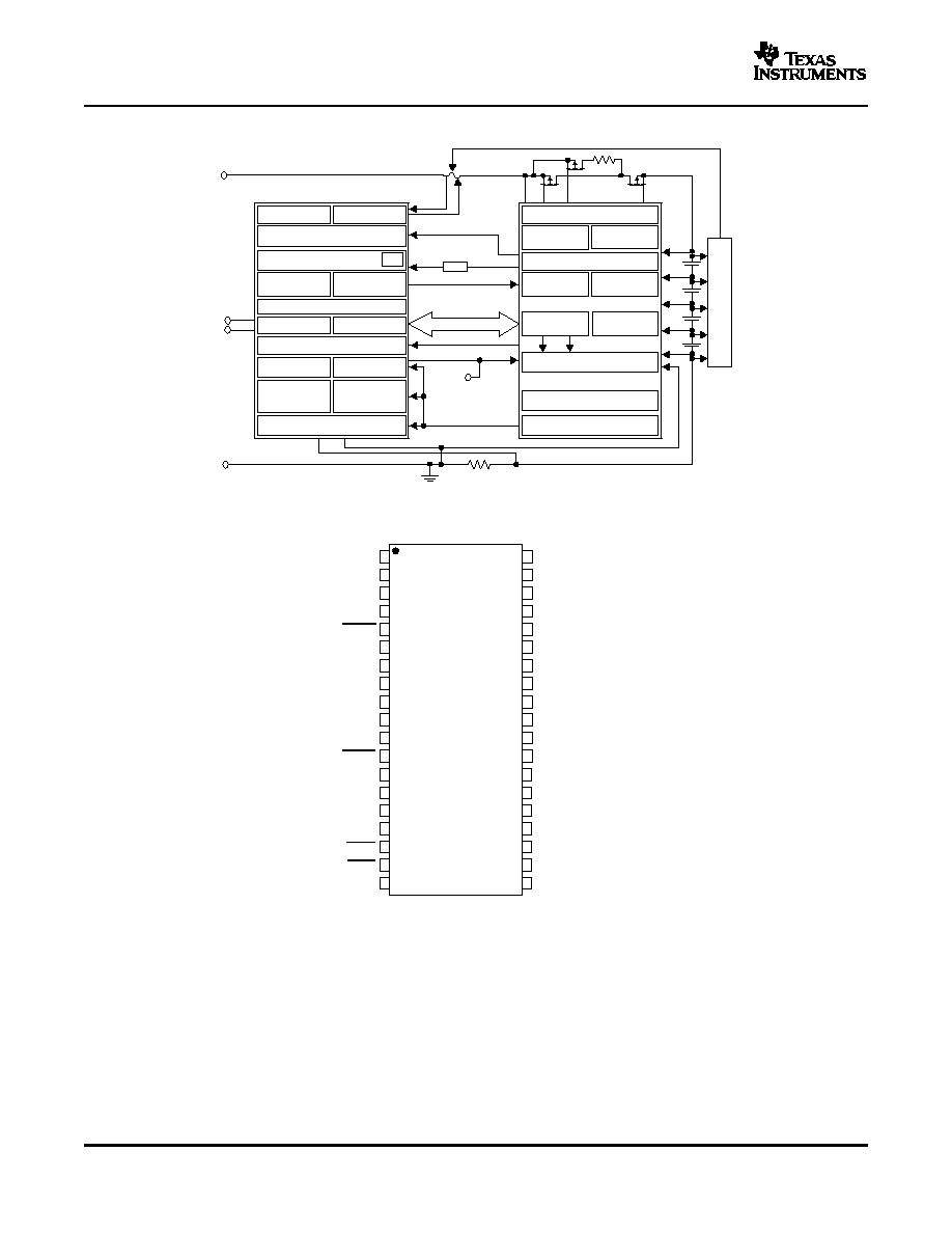
SYSTEM PARTITIONING DIAGRAM
LDO, Therm Output Drive & UVLO
Power Management
LDO, TOUT, and Power Mode control
I2C
Impedance Track (TM) + Lifetime Data Logging
SMBus
Pack +
Pack -
Discharge / Charge /
Precharge FETs
Cell and Pack
Voltage
Measurement
Precharge
FET Drive
2-Tier Overcurrent Protection
32-kHz Clock
Generator
bq20z80
768 Bytes of
User Flash
Fuse
1stLevel OV and
UV Protection
Pack Undervoltage
Power Mode
Control
Precharge Control
Delay Counters
Cell Balancing Algorithm and Control
Cell Balancing
Drive
System Interface
System Watchdog
Voltage Level Translator
System Interface
32 kHz
Power Mode Control
Fail-Safe Protection
T1
1st Level OC
Protection
Temperature Measurement
<1% Error
TINT
Supply V oltage
bq29312A
PCH FET Drive
RAM Registers
SBS v1.1 Data
bq29312 RAM/Comms Validation
2 nd Level Overvoltage Protection
bq294xx
XAlert
Sleep
Sense Resistor
(5 m - 20 mW typ)
PF Input
1
2
7
6
5
4
3
38
37
36
35
34
33
32
VIN
TS1
TS2
PU
PRES
SCLK
VSSD
NC
NC
CLKOUT
XCK1 / VSSA
XCK2 / ROSC
FILT
SAFE
VDDD
VDDA
RBI
SDATA
VSSD
SAFE
SR2
SR1
VSSA
VSSA
8
9
10
11
12
31
30
29
28
27
13
14
19
18
17
16
15
26
25
24
23
22
21
20
NC
NC
SMBC
SMBD
DISP
PFIN
MRST
XALERT
LED1
LED2
LED3
LED4
LED5
VSSD
NC - No internal connection
bq20z80-V102
SLUS681A NOVEMBER 2005 REVISED MARCH 2006
TSSOP (DBT)
(TOP VIEW)
2
Submit Documentation Feedback

www.ti.com
bq20z80-V102
SLUS681A NOVEMBER 2005 REVISED MARCH 2006
TERMINAL FUNCTIONS
TERMINAL
I/O
(1)
DESCRIPTION
NO.
NAME
1
VIN
I
Voltage measurement input from the AFE
2
TS1
I
1
st
Thermistor voltage input connection to monitor temperature
3
TS2
I
2
nd
Thermistor voltage input connection to monitor temperature
4
PU
O
Output to pull up the PRES pin for system detection
5
PRES
I
Active low input to sense system insertion and typically requires additional ESD protection
6
SCLK
I/OD
Communication clock to the AFE
7
SAFE
O
Active high output to enforce additional level of safety protection; e.g., fuse blow. (Inverse of pin 12)
8
VDDD
P
Positive supply for digital circuitry and I/O pins
Backup power to the bq20z80 data registers during periods of low operating voltage. RBI accepts a
9
RBI
P
storage capacitor or a battery input.
10
SDATA
I/O
Data transfer to and from the AFE
12
SAFE
O
Active low output to enforce additional level of safety protection; e.g., fuse blow. (Inverse of pin 7)
13
NC
Not used-- leave floating
14
NC
Not used-- leave floating
15
SMBC
I/OD
SMBus clock open-drain bidirectional pin used to clock the data transfer to and from the bq20z80
16
SMBD
I/OD
SMBus data open-drain bidirectional pin used to transfer address and data to and from the bq20z80
Display control for the LEDs. This pin is typically connected to bq29312A REG via a 100-k
resistor
17
DISP
I
and a push-button switch to VSSD.
Active low input to detect secondary protector output status and allows the bq20z80 to report the
18
PFIN
I
status of the 2
nd
level protection output
20
LED5
O
LED5 display segment that drives an external LED depending on the firmware configuration
21
LED4
O
LED4 display segment that drives an external LED depending on the firmware configuration
22
LED3
O
LED3 display segment that drives an external LED depending on the firmware configuration
23
LED2
O
LED2 display segment that drives an external LED depending on the firmware configuration
24
LED1
O
LED1 display segment that drives an external LED depending on the firmware configuration
25
XALERT
I
Input from bq29312A XALERT output.
26
MRST
I
Master reset input that forces the device into reset when held high
Connections for a small-value sense resistor to monitor the battery charge- and discharge-current
27
SR2
IA
flow
Connections for a small-value sense resistor to monitor the battery charge- and discharge-current
28
SR1
IA
flow
31
VDDA
P
Positive supply for analog circuitry
Analog input connected to the external PLL filter components which are a 150-pF capacitor to V
SSA
,
32
FILT
IA
in parallel with a 61.9-k
resistor and a 2200-pF capacitor in series. Place these components as
close as possible to the bq20z80 to ensure optimal performance.
32.768-kHz crystal oscillator output pin or connected to a 100k, 50ppm or better resistor if the
33
XCK2/ROSC
O
internal oscillator is used
34
XCK1/VSSA
I
32.768-kHz crystal oscillator input pin or connected to VSSA if the internal oscillator is used
35
CLKOUT
O
32.768-kHz output for the bq29312. This pin should be directly connected to the AFE.
36, 37
NC
-
Not used-- leave floating
11, 19, 38
VSSD
P
Negative supply for digital circuitry
29, 30
VSSA
P
Negative supply for analog circuitry.
(1)
I = Input, IA = Analog input, I/O = Input/output, I/OD = Input/Open-drain output, O = Output, OA = Analog output, P = Power
3
Submit Documentation Feedback
www.ti.com
ABSOLUTE MAXIMUM RATINGS
ELECTRICAL CHARACTERISTICS
bq20z80-V102
SLUS681A NOVEMBER 2005 REVISED MARCH 2006
over operating free-air temperature range (unless otherwise noted)
(1)
RANGE
V
DDA
and V
DDD
relative to V
SS
(2)
Supply voltage range
0.3 V to 4.1 V
V
(IOD)
relative to V
SS
(2)
Open-drain I/O pins
0.3 V to 6 V
V
I
relative to V
SS
(2)
Input voltage range to all other pins
0.3 V to VDDA + 0.3 V
T
A
Operating free-air temperature range
40
°
C to 85
°
C
T
stg
Storage temperature range
65
°
C to 150
°
C
(1)
Stresses beyond those listed under absolute maximum ratings may cause permanent damage to the device. These are stress ratings
only, and functional operation of the device at these or any other conditions beyond those indicated under recommended operating
conditions is not implied. Exposure to absolute-maximum-rated conditions for extended periods may affect device reliability.
(2)
V
SS
refers to the common node of V
(SSA)
and V
(SSD)
.
V
DD
= 3 V to 3.6 V, T
A
= 40
°
C to 85
°
C (unless otherwise noted)
PARAMETER
TEST CONDITIONS
MIN
TYP
MAX
UNIT
V
DD
Supply voltage
VDDA and VDDD
3
3.3
3.6
V
No flash programming
350
(1)
I
DD
Operating mode current
µ
A
bq20z80 + bq29312A
375
Sleep mode
8
(1)
I
(SLP)
Low-power storage mode current
µ
A
bq20z80 + bq29312A
28
Shutdown Mode
0.1
(1)
I
(SLP)
Shutdown Current
µ
A
bq20z80 + bq29312A
0.2
Output voltage low SMBC, SMBD, SDATA, SCLK, SAFE,
I
OL
= 0.5 mA
0.4
V
SAFE, PU
V
OL
LED1 LED5
I
OL
= 10 mA
0.4
V
V
OH
Output high voltage, SMBC, SMBD, SDATA, SCLK, SAFE,
I
OH
= 1 mA
V
DD
0.5
V
SAFE, PU
V
IL
Input voltage low SMBC, SMBD, SDATA, SCLK, XALERT,
0.3
0.8
V
PRES, PFIN
DISP
0.3
0.8
V
V
IH
Input voltage high SMBC, SMBD, SDATA, SCLK, XALERT,
2
6
V
PRES, PFIN
DISP
2
V
CC
+ 0.3
V
C
IN
Input capacitance
5
pF
V
(AI1)
Input voltage range VIN, TS1, TS2
V
SS
0.3
1
V
V
(AI2)
Input voltage range SR1, SR2
V
SS
0.25
0.25
Z
(AI1)
Input impedance SR1, SR2
0 V1 V
2.5
M
Z
(AI2)
Input impedance VIN, TS1, TS2
0 V1 V
8
M
(1)
This value does not include the bq29312A
4
Submit Documentation Feedback
www.ti.com
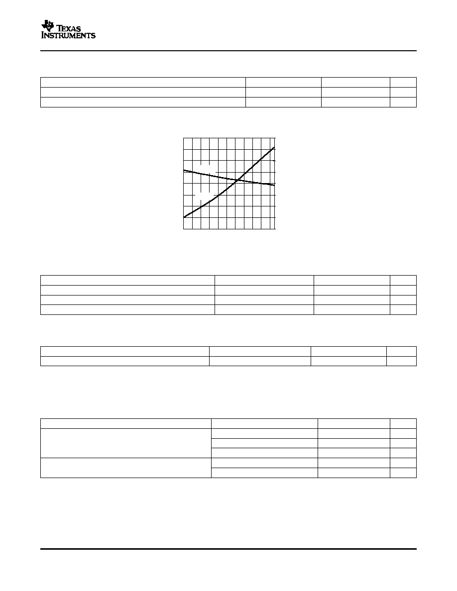
POWER-ON RESET
2.10
2.15
2.20
2.25
2.30
2.35
2.40
2.45
2.50
-20 -10
0
10 20 30 40 50 60 70 80
100
105
110
115
120
125
130
135
140
T
A
- Free-Air Temperature -
°
C
- Negative Going Input Threshold V
oltage - V
POWER ON RESET BEHAVIOR
vs
FREE-AIR TEMPERATURE
V
IT
V
IT-
V
hys
V
hys
- Hysterisis V
oltage - mV
INTEGRATING ADC (Coulomb Counter) CHARACTERISTICS
PLL SWITCHING CHARACTERISTICS
OSCILLATOR
bq20z80-V102
SLUS681A NOVEMBER 2005 REVISED MARCH 2006
V
DD
= 3 V to 3.6 V, T
A
= 40
°
C to 85
°
C (unless otherwise noted)
PARAMETER
TEST CONDITIONS
MIN
TYP
MAX
UNIT
V
IT
Negative-going voltage input
2.1
2.3
2.5
V
V
HYS
Power-on reset hysteresis
50
150
200
mV
V
DD
= 3 V to 3.6 V, T
A
= 40
°
C to 85
°
C (unless otherwise noted)
PARAMETER
TEST CONDITIONS
MIN
TYP
MAX
UNIT
V
(SR)
Input voltage range, V
(SR2)
and V
(SR1)
V
(SR)
= V(SR2) V(SR1)
0.25
0.25
V
V
(SROS)
Input offset
1
µ
V
INL
Integral nonlinearity error
0.004%
0.019%
V
DD
= 3 V to 3.6 V, T
A
= 40
°
C to 85
°
C (unless otherwise noted)
PARAMETER
TEST CONDITIONS
MIN
TYP
MAX
UNIT
t
(SP)
Start-up time
(1)
0.5% frequency error
2
5
ms
(1)
The frequency error is measured from the trimmed frequency of the internal system clock which is 128 oscillator frequency, nominally
4.194 MHz.
V
DD
= 3 V to 3.6 V, T
A
= 40
°
C to 85
°
C (unless otherwise noted)
PARAMETER
TEST CONDITIONS
MIN
TYP
MAX
UNIT
ROSC = 100 k
2%
0.25%
2%
f
(exo)
Frequency error from 32.768 kHz
ROSC = 100 k
, V
DD
= 3.3 V
1%
0.25%
1%
XCK1 = 12-pF XTAL
0.25%
0.25%
f
(sxo)
Start-up time
(1)
ROSC = 100 k
250
µ
s
XCK1 = 12-pF XTAL
200
ms
(1)
The start-up time is defined as the time it takes for the oscillator output frequency to be within 1% of the specified frequency.
5
Submit Documentation Feedback
Document Outline