
Features
‰ Power monitoring and switching
for 3-volt battery-backup applica-
tions
‰ Write-protect control
‰ 2-input decoder for control of up
to 4 banks of SRAM
‰ 3-volt primary cell inputs
‰ Less than 10ns chip-enable
propagation delay
‰ 5% or 10% supply operation
General Description
The CMOS bq2204A SRAM Non-
volatile Controller Unit provides all
necessary functions for converting
up to four banks of standard CMOS
SRAM into nonvolatile read/write
memory.
A precision comparator monitors the 5V
V
CC
input for an out-of-tolerance condi-
tion. When out-of-tolerance is detected,
the four conditioned chip-enable outputs
are forced inactive to write-protect up to
four banks of SRAM.
During a power failure, the external
SRAMs are switched from the V
CC
supply to one of two 3V backup sup-
plies. On a subsequent power-up, the
SRAMs are write-protected until a
power-valid condition exists.
During power-valid operation, a
two-input decoder transparently se-
lects one of up to four banks of
SRAM.
1
Dec. 1992 B
bq2204A
X4 SRAM Nonvolatile Controller Unit
1
PN220401.eps
16-Pin Narrow DIP or SOIC
2
3
4
5
6
7
8
16
15
14
13
12
11
10
9
VCC
BC1
CE
CECON1
CECON2
CECON3
CECON4
NC
VOUT
BC2
NC
A
B
NC
THS
VSS
Pin Names
V
OUT
Supply output
BC
1
≠BC
2
3 volt primary backup cell inputs
THS
Threshold select input
CE
chip-enable active low input
CE
CON1
≠
Conditioned chip-enable outputs
CE
CON4
A≠B
Decoder inputs
NC
No connect
V
CC
+5 volt supply input
V
SS
Ground
Up to four banks of CMOS static RAM can be battery-
backed using the V
OUT
and conditioned chip-enable out-
put pins from the bq2204A. As V
CC
slews down during
a power failure, the conditioned chip-enable outputs
CE
CON1
through CE
CON4
are forced inactive independ-
ent of the chip-enable input CE.
This activity unconditionally write-protects the external
SRAM as V
CC
falls below an out-of-tolerance threshold
V
PFD
. V
PFD
is selected by the threshold select input pin,
THS. If THS is tied to V
SS
, the power-fail detection occurs
at 4.62V typical for 5% supply operation.
If THS is tied to V
CC
, power-fail detection occurs at
4.37V typical for 10% supply operation. The THS pin
must be tied to V
SS
or V
CC
for proper operation.
If a memory access is in process to any of the four external
banks of SRAM during power-fail detection, that memory
cycle continues to completion before the memory is write-
protected. If the memory cycle is not terminated
within
time t
WPT
, all four chip-enable outputs are unconditionally
driven high, write-protecting the controlled SRAMs.
Pin Connections
Functional Description
As the supply continues to fall past V
PFD
, an internal
switching device forces V
OUT
to one of the two external
backup energy sources.
CE
CON1
through CE
CON4
are
held high by the V
OUT
energy source.
During power-up, V
OUT
is switched back to the 5V sup-
ply as V
CC
rises above the backup cell input voltage
sourcing V
OUT
. Outputs CE
CON1
through CE
CON4
are
held inactive for time t
CER
(120ms maximum) after the
power supply has reached V
PFD
, independent of the CE
input, to allow for processor stabilization.
During power-valid operation, the CE input is passed
through to one of the four CE
CON
outputs with a propa-
gation delay of less than 10ns. The CE input is output
on one of the four CE
CON
output pins depending on the
level of the decode inputs at A and B as shown in the
Truth Table.
The A and B inputs are usually tied to high-order ad-
dress pins so that a large nonvolatile memory can be de-
signed using lower-density memory devices. Nonvolatility
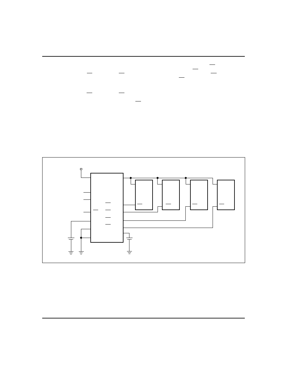
and decoding are achieved by hardware hookup as shown
in Figure 1.
2
bq2204A
FG220401.eps
CE
BC2
THS
VSS
VOUT
bq2204A
VCC
CE
CMOS
SRAM
VCC
5V
From Address
Decoder
CECON2
BC1
CECON1
VCC
CE
CMOS
SRAM
3V
Primary
Cell
3V
Primary
Cell
B
A
VCC
CE
CMOS
SRAM
VCC
CE
CMOS
SRAM
CECON3
CECON4
Figure 1. Hardware Hookup (5% Supply Operation)
Dec. 1992 B

Energy Cell Inputs--BC
1
, BC
2
Two backup energy source inputs are provided on the
bq2204A. The BC
1
and BC
2
inputs accept a 3V primary
battery (non-rechargeable), typically some type of lith-
ium chemistry. If no primary cell is to be used on either
BC
1
or BC
2
, the unused input should be tied to V
SS
.
V
CC
falling below V
PFD
starts the comparison of BC
1
and BC
2
. The BC input comparison continues until V
CC
rises above V
SO
. Power to V
OUT
begins with BC
1
and
switches to BC
2
only when V
BC1
is less than V
BC2
mi-
nus V
BSO
. The controller alternates to the higher BC
voltage only when the difference between the BC input
voltages is greater than V
BSO
. Alternating the backup
batteries allows one-at-a-time battery replacement and
efficient use of both backup batteries.
To prevent battery drain when there is no valid data to
retain, V
OUT
and CE
CON1-4
are internally isolated from
BC
1
and BC
2
by either of the following conditions:
s
Initial connection of a battery to BC
1
or BC
2,
or
s
Presentation of an isolation signal on CE.
A valid isolation signal requires CE low as V
CC
crosses
both V
PFD
and V
SO
during a power-down. See Figure 2.
Between these two points in time, CE must be brought
to the point of (0.48 to 0.52)*V
CC
and held for at least
700ns.
The isolation signal is invalid if CE exceeds
0.54*V
CC
at any point between V
CC
crossing V
PFD
and
V
SO
.
The appropriate battery is connected to V
OUT
and
CE
CON1≠4
immediately on subsequent application and
removal of V
CC
.
3
TD220201.eps
VCC
CE
VPFD
VSO
0.5 VCC
700ns
Figure 2. Battery Isolation Signal
Dec. 1992 B
Truth Table
Input
Output
CE
A
B
CE
CON1
CE
CON2
CE
CON3
CE
CON4
H
X
X
H
H
H
H
L
L
L
L
H
H
H
L
H
L
H
L
H
H
L
L
H
H
H
L
H
L
H
H
H
H
H
L
bq2204A

4
bq2204A
Recommended DC Operating Conditions
(TA = TOPR)
Symbol
Parameter
Minimum
Typical
Maximum
Unit
Notes
V
CC
Supply voltage
4.75
5.0
5.5
V
THS = V
SS
4.50
5.0
5.5
V
THS = V
CC
V
SS
Supply voltage
0
0
0
V
V
IL
Input low voltage
-0.3
-
0.8
V
V
IH
Input high voltage
2.2
-
V
CC
+ 0.3
V
V
BC1
,
V
BC2
Backup cell voltage
2.0
-
4.0
V
V
CC
< V
BC
THS
Threshold select
-0.3
-
V
CC
+ 0.3
V
Note:
Typical values indicate operation at T
A
= 25∞C, V
CC
= 5V or V
BC
.
Absolute Maximum Ratings
Symbol
Parameter
Value
Unit
Conditions
V
CC
DC voltage applied on V
CC
relative to V
SS
-0.3 to +7.0
V
V
T
DC voltage applied on any pin excluding V
CC
relative to V
SS
-0.3 to +7.0
V
V
T
V
CC
+ 0.3
T
OPR
Operating temperature
0 to 70
∞C
Commercial
-40 to +85
∞C
Industrial "N"
T
STG
Storage temperature
-55 to +125
∞C
T
BIAS
Temperature under bias
-40 to +85
∞C
T
SOLDER
Soldering temperature
260
∞C
For 10 seconds
I
OUT
V
OUT
current
200
mA
Note:
Permanent device damage may occur if Absolute Maximum Ratings are exceeded. Functional operation
should be limited to the Recommended DC Operating Conditions detailed in this data sheet. Exposure to con-
ditions beyond the operational limits for extended periods of time may affect device reliability.
Dec. 1992 B

5
DC Electrical Characteristics
(TA = TOPR, VCC = 5V
±
10%)
Symbol
Parameter
Minimum
Typical
Maximum
Unit
Conditions/Notes
I
LI
Input leakage current
-
-
±
1
µ
A
V
IN
= V
SS
to V
CC
V
OH
Output high voltage
2.4
-
-
V
I
OH
= -2.0mA
V
OHB
V
OH
, BC supply
V
BC
- 0.3
-
-
V
V
BC
> V
CC
, I
OH
= -10
µ
A
V
OL
Output low voltage
-
-
0.4
V
I
OL
= 4.0mA
I
CC
Operating supply current
-
3
6
mA
No load on outputs.
V
PFD
Power-fail detect voltage
4.55
4.62
4.75
V
THS = V
SS
4.30
4.37
4.50
V
THS = V
CC
V
SO
Supply switch-over voltage
-
VBC
-
V
I
CCDR
Data-retention mode
current
-
-
100
nA
V
OUT
data-retention current
to additional memory not in-
cluded.
V
BC
Active backup cell
voltage
-
V
BC1
-
V
V
BC1
> V
BC2
+ V
BSO
-
V
BC2
-
V
V
BC2
> V
BC1
+ V
BSO
V
BSO
Battery switch-over voltage
0.25
0.4
0.6
V
I
OUT1
V
OUT
current
-
-
160
mA
V
OUT
> V
CC
- 0.3V
I
OUT2
V
OUT
current
-
100
-
µ
A
V
OUT
> V
BC
- 0.2V
Note:
Typical values indicate operation at T
A
= 25∞C, V
CC
= 5V or V
BC
.
Capacitance
(TA = 25∞C, F = 1MHz, VCC = 5.0V)
Symbol
Parameter
Minimum
Typical
Maximum
Unit
Conditions
C
IN
Input capacitance
-
-
8
pF
Input voltage = 0V
C
OUT
Output capacitance
-
-
10
pF
Output voltage = 0V
Note:
This parameter is sampled and not 100% tested.
Dec. 1992 B
bq2204A