bq2205LY
SLUS581 - FEBRUARY 2004
POWER MONITORING AND SWITCHING CONTROLLER
FOR 3.3 V SRAM
1
www.ti.com
FEATURES
D
Power Monitoring and Switching for
Non-Volatile Control of SRAMs
D
Input Decoder Allows Control of 1 or 2 Banks
of SRAM
D
Write-Protect Control
D
3-V Primary Cell Input
D
3.3-V Operation
D
Reset Output for System Power-On Reset
D
Less than 20-ns Chip Enable Propagation
Delay
D
Small 16-Lead TSSOP Package
APPLICATIONS
D
NVSRAM Modules
D
Point-of-Sale Systems
D
Facsimile, Printers and Photocopiers
D
Internet Appliances
D
Servers
D
Medical Instrumentation and Industrial
Products
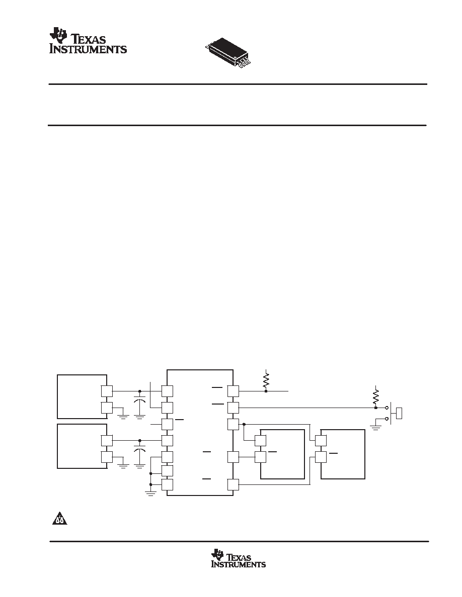
DESCRIPTION
The CMOS bq2205 SRAM non-volatile controller
with reset provides all the necessary functions for
converting one or two banks of standard CMOS
SRAM into non-volatile read/write memory.
A precision comparator monitors the 3.3-V VCC
input for an out-of-tolerance condition. When
out-of-tolerance is detected, the two conditioned
chip-enable outputs are forced inactive to
write-protect both banks of SRAM.
Power for the external SRAMs, VOUT, is switched
from the VCC supply to the battery-backup supply
as VCC decays. On a subsequent power-up, the
VOUT supply is automatically switched from the
backup supply to the VCC supply. The external
SRAMs are write-protected until a power-valid
condition exists. The reset output provides
power-fail and power-on resets for the system.
During power-valid operation, the input decoder, A,
selects one of two banks of SRAM.
UDG-03129
VCC
VSS
RST
CECON2
CECON1
VCC
VCC
CE
CE
CE
12
1
4
13
10
VOUT
VCC
A
bq2205LYPW
11
9
14
16
VCC
SRAM Bank 2
VCC
SRAM Bank 1
To Microprocessor
15
VDC
GND
Backup Supply
VDC
GND
Main Supply
5
8
Pushbutton
Reset
(Optional)
BW
VSS
VSS
BCP
From Address
Selector
PRODUCTION DATA information is current as of publication date.
Products conform to specifications per the terms of Texas Instruments
standard warranty. Production processing does not necessarily include
testing of all parameters.
Copyright
2004, Texas Instruments Incorporated
Please be aware that an important notice concerning availability, standard warranty, and use in critical applications of Texas Instruments
semiconductor products and disclaimers thereto appears at the end of this data sheet.
bq2205LY
SLUS581 - FEBRUARY 2004
2
www.ti.com
These devices have limited built-in ESD protection. The leads should be shorted together or the device placed in conductive foam
during storage or handling to prevent electrostatic damage to the MOS gates.
ORDERING INFORMATION
TA
OPERATION
PART NUMBER(1)
SYMBOL
- 20
�
C to 70
�
C
3.3 V
bq2205LYPW
bq2205LY
(1) The PW package is available taped and reeled. Add an R suffix to the device type (i.e. bq2205LYPWR) to order quantities of 2,000 devices
per reel.
ABSOLUTE MAXIMUM RATINGS
over operating free-air temperature range unless otherwise noted(2)
bq2205LY
UNIT
VCC, (wrt VSS)
-0.3 to 6.0
Input voltage range
BCP, (wrt VSS)
-0.3 to 4.5
V
Input voltage range
all other pins, (wrt VSS)
-0.3 to VCC + 0.3
V
Operating temperature range, TA
-20 to 70
Storage temperature, Tstg
-55 to 125
�
C
Temperature under bias, TJbias
-40 to 85
�
C
Lead temperature 1,6 mm (1/16 inch) from case for 10 seconds
300
(2) Stresses beyond those listed under "absolute maximum ratings" may cause permanent damage to the device. These are stress ratings only,
and functional operation of the device at these or any other conditions beyond those indicated under "recommended operating conditions"
is not implied. Exposure to absolute-maximum-rated conditions for extended periods may affect device reliability.
RECOMMENDED OPERATING CONDITIONS
MIN
MAX
UNIT
Supply voltage, VCC
3.0
3.6
Supply voltage from backup cell, VBC
2.0
4.0
Low-level input voltage, VIL
-0.3
0.8
V
High-level input voltage, VIH
2.2
VCC + 0.3
V
RST low-level input voltage, VIL
-0.3
0.4
RST high-level input voltage, VIH
2.2
VCC + 0.3
Operating temperature range, TA
-20
70
�
C

bq2205LY
SLUS581 - FEBRUARY 2004
3
www.ti.com
ELECTRICAL CHARACTERISTICS
(TA = 25
�
C, VCC(min)
VCC
VCC(max) unless otherwise noted)
PARAMETER
TEST CONDITIONS
MIN
TYP
MAX
UNIT
VCC supply current, ICC(vcc)
VCC > VCC(MIN)
CE = low
CECONX = 0 mA
210
500
�
A
Backup Battery Supply Current, ICC(BC)
VBC > VBC(MIN), VCC = 0 V
CE = low
CECONX = 0 mA
50
150
nA
Output voltage (VOUT)
I(VOUT) = 80 mA, VCC > V(SO)
Vcc-0.3
Output voltage (VOUT)
I(VOUT)= 100
�
A, VCC < V(SO)
VBC-0.3
Power fail detect voltage, VPFD
2.85
2.9
2.95
Supply switch-over voltage, VSO
VBC > V(PFD)
VPFD
V
Supply switch-over voltage, VSO
VBC < V(PFD)
VBC
V
RST output voltage
I(RST) = 1 mA
0.4
BW output voltage
I(BW)= 1 mA
0.4
Input leakage current on A and CE pins
-1
1
�
A
Voh CEcon1,2
Ioh = 0.5 mA
2.4
Vol CEcon1,2
Iol = 2.0 mA
0.4
V
Battery warning level VBW
(1)
0.677xVCC
V
Capacitance
Output capacitance
VOUT = 0 V
7
pF
Input capacitance
VOUT = 0 V
5
pF
Power-Down and Power-Up Timing, Refer to Figure 1 through 3
VCC slew rate fall time, tF
3.0 V to 0.0 V
300
s
VCC slew rate rise time, tR
VSO to VPFD(max)
100
�
s
VPFD to RST active, tRST
(reset active timeout period)
30
85
ms
Chip-enable recovery time, tCER
(2)
30
85
ms
Chip-enable propagation delay time to external
SRAM, tCED
See Figure 2
15
25
ns
Push-button low time, tPBL
RST pin
1
�
s
(1)
Battery warning level is detected on power up and the BW pin is latched at tCER time after VCC passes through VPFD on power up.
(2)
Time during which external SRAM is write protected after VCC passes through VPFD on power up.

bq2205LY
SLUS581 - FEBRUARY 2004
4
www.ti.com
AC TEST CONDITIONS, INPUT PULSE LEVELS 0 V
V
IN
3 V, t
R
= t
F
= 5 NS
Figure 1. Output Load
CL
TTL
(including scope
and JIG)
CECONX
VCC
VCC
VPFD
VSO
tF
VSO
VPFD
VPFD(max)
tR
CE
CECONX
tCED
tRST
tCER
tCED
RST
Figure 2. Power-Down/Power-Up Timing Diagram
VPBRL
RST
tPBL
tRST
VPBRH
Figure 3. Push-Button Reset Timing

bq2205LY
SLUS581 - FEBRUARY 2004
5
www.ti.com
TERMINAL FUNCTIONS
NAME
TERMINAL
I/O
DESCRIPTION
NAME
bq2205LY
I/O
DESCRIPTION
A
1
I
SRAM bank select input
BCP
9
I
Backup supply input
BW
15
O
Battery warning output (open-drain)
CE
11
I
Chip enable input (active low)
CECON1
10
O
Conditioned chip enable output 1
CECON2
14
O
Conditioned chip enable output 2
N/C
2, 3, 6, 7
-
No connect. These pins must be left floating.
RST
16
O
Power-up reset to system CPU output (open-drain)
VCC
12
I
Main supply input
VOUT
13
O
SRAM supply output
VSS
4, 5, 8
-
Ground input
1
2
3
4
5
6
7
8
16
15
14
13
12
11
10
9
A
N/C
N/C
V
SS
V
SS
N/C
N/C
V
SS
RST
BW
CE
CON2
V
OUT
V
CC
CE
CE
CON1
BC
P
PW PACKAGE
(TOP VIEW)
N/C no connection