
bq24007
bq24008
SLUS479D - JANUARY 2001 - REVISED NOVEMBER 2004
SINGLE CELL Li ION CHARGE MANAGEMENT IC WITH
TIMER ENABLE FOR PDAs AND INTERNET APPLIANCES
FEATURES
D
Highly Integrated Solution With FET Pass
Transistor and Reverse-Blocking Schottky
and Thermal Protection
D
Timer-Enable Function That Allows Host to
Disable Charge Timer and Termination When
Charge Current Is Shared With a Load or
When Battery Is Absent
D
Integrated Voltage and Current Regulation
With Programmable Charge Current
D
High-Accuracy Voltage Regulation (
±
1%)
D
Ideal for Low-Dropout Linear Charger
Designs for Single-Cell Li-Ion Packs With
Coke or Graphite Anodes
D
Up to 1.2-A Continuous Charge Current
D
Safety-Charge Timer During Preconditioning
and Fast Charge
D
Integrated Cell Conditioning for Reviving
Deeply Discharged Cells and Minimizing Heat
Dissipation During Initial Stage of Charge
D
Optional Temperature or Input-Power
Monitoring Before and During Charge
D
Various Charge-Status Output Options for
Driving Single, Double, or Bicolor LEDs or
Host-Processor Interface
D
Charge Termination by Minimum Current and
Time
D
Low-Power Sleep Mode
D
Packaging: 5 mm
◊
5 mm MLP (bq24007)or
20-Lead TSSOP PowerPAD
APPLICATIONS
D
PDAs
D
Internet Appliances
D
MP3 Players
D
Digital Cameras
DESCRIPTION
The bq2400x series ICs are advanced Li-Ion linear
charge management devices for highly integrated and
space-limited applications. They combine high-
accuracy current and voltage regulation; FET pass-
transistor and reverse-blocking Schottky; battery
conditioning, temperature, or input-power monitoring;
charge termination; charge-status indication; and
charge timer in a small package.
The bq24007 and bq24008 provide the timer-enable
function, allowing the host to disable the charge timer
when charge current is shared with a load or when the
battery is absent. This feature is ideal for applications
such as cellular phones, PDAs, and internet
appliances.
The bq2400x measures battery temperature using an
external thermistor. For safety reasons, the bq2400x
inhibits charge until the battery temperature is within the
user-defined thresholds. Alternatively, the user can
monitor the input voltage to qualify charge. The
bq2400x series then charge the battery in three phases:
preconditioning, constant current, and constant
voltage. If the battery voltage is below the internal
low-voltage threshold, the bq2400x uses low-current
precharge to condition the battery. A preconditioning
timer provides additional safety. Following pre-
conditioning, the bq2400x applies a constant-charge
current to the battery. An external sense-resistor sets
the magnitude of the current. The constant-current
phase is maintained until the battery reaches the
charge-regulation voltage. The bq2400x then
transitions to the constant voltage phase. The user can
configure the device for cells with either coke or
graphite anodes. The accuracy of the voltage regulation
is better than
±
1% over the operating junction
temperature and supply voltage range.
Charge is terminated by maximum time or minimum
taper current detection
The bq2400x automatically restarts the charge if the
battery voltage falls below an internal recharge
threshold.
PowerPAD is a trademark of Texas Instruments.
PRODUCTION DATA information is current as of publication date. Products
conform to specifications per the terms of Texas Instruments standard warranty.
Production processing does not necessarily include testing of all parameters.
Please be aware that an important notice concerning availability, standard warranty, and use in critical applications of Texas Instruments
semiconductor products and disclaimers thereto appears at the end of this data sheet.
www.ti.com
Copyright
2002 - 2004, Texas Instruments Incorporated

bq24007
bq24008
SLUS479D - JANUARY 2001 - REVISED NOVEMBER 2004
www.ti.com
2
These devices have limited built-in ESD protection. The leads should be shorted together or the device placed in conductive foam during
storage or handling to prevent electrostatic damage to the MOS gates.
ORDERING INFORMATION
PACKAGE
CHARGE STATUS
TJ
20-LEAD HTTSOP PowerPAD
(PWP)(1)
20-LEAD 5 mm
◊
5 mm MLP
(RGW)(2)
CHARGE STATUS
CONFIGURATION
-40
∞
C to 125
∞
C
bq24007PWP
bq24007RGW
Single LED
-40
∞
C to 125
∞
C
bq24008PWP
Not available
Single bicolor LED
(1) The PWP package is available taped and reeled. Add R suffix to device type (e.g. bq24007PWPR) to order. Quantities 2500 devices per reel.
(2) The RGW package is available taped and reeled. Add R suffix to device type (e.g. bq24007RGWR) to order. Quantities 3000 devices per reel.
PACKAGE DISSIPATION RATINGS
PACKAGE
JA
JC
TA
25
∞
C
POWER RATING
DERATING FACTOR
ABOVE TA = 25
∞
C
PWP(1)
30.88
∞
C/W
1.19
∞
C/W
3.238 W
0.0324W/
∞
C
RGW(2)
31.41
∞
C/W
1.25
∞
C/W
3.183 W
0.0318W/
∞
C
(1) This data is based on using the JEDEC high-K board and topside traces, top and bottom thermal pad (6,5
◊
3,4 mm), internal 1 oz power and
ground planes, 8 thermal via underneath the die connecting to ground plane.
(2) This data is based on using the JEDEC high-K board and topside traces, top and bottom thermal pad (3,25
◊
3,25 mm), internal 1 oz power
and ground planes, 9 thermal via underneath the die connecting to ground plane.
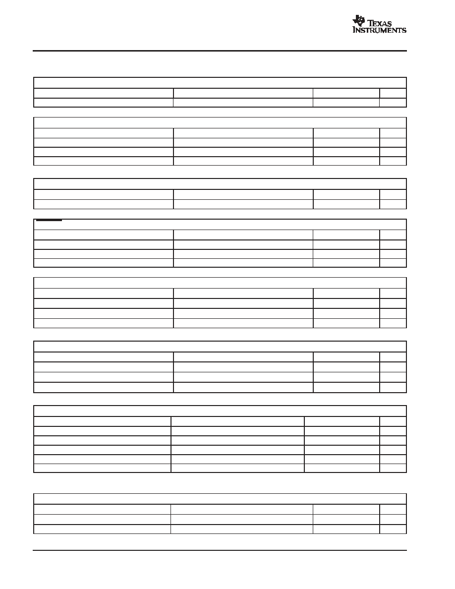
ABSOLUTE MAXIMUM RATINGS
over operating free-air temperature range unless otherwise noted(1)
bq24007
bq24008
Supply voltage (VCC with respect to GND)
13.5 V
Input voltage (IN, ISNS, TMR EN, APG/THERM/CR/STAT1/STAT2, VSENSE, TMR SEL, VSEL) (all with respect to GND)
13.5 V
Output current (OUT pins)
2 A
Output sink/source current (STAT1 and STAT2)
10 mA
Operating free-air temperature range, TA
-40
∞
C to 70
∞
C
Storage temperature range, Tstg
-65
∞
C to 150
∞
C
Junction temperature range, TJ
-40
∞
C to 125
∞
C
Lead temperature (Soldering, 10 s)
300
∞
C
(1) Stresses beyond those listed under "absolute maximum ratings" may cause permanent damage to the device. These are stress ratings only, and
functional operation of the device at these or any other conditions beyond those indicated under "recommended operating conditions" is not
implied. Exposure to absolute-maximum-rated conditions for extended periods may affect device reliability.
RECOMMENDED OPERATING CONDITIONS
MIN
MAX
UNIT
Supply voltage, VCC
4.5
10
V
Input voltage, VIN
4.5
10
V
Continuous output current
1.2
A
Operating junction temperature range, TJ
-40
125
∞
C

bq24007
bq24008
SLUS479D - JANUARY 2001 - REVISED NOVEMBER 2004
www.ti.com
3
ELECTRICAL CHARACTERISTICS
over recommended operating junction temperature supply and input voltages, and VI (VCC)
VI (IN) ( unless otherwise noted)
PARAMETER
TEST CONDITIONS
MIN
TYP
MAX
UNIT
VCC current
VCC > VCC_UVLO
1
mA
Standby current (sum of currents into OUT
and VSENSE pins)
VCC < VCC_UVLO,
VO(OUT) = 4.3 V,
VSENSE = 4.3 V
2
4
µ
A
VOLTAGE REGULATION, 0
∞
C
T
J
125
∞
C
PARAMETER
TEST CONDITIONS
MIN
TYP
MAX
UNIT
Output voltage
VSEL = VSS,
0 < IO
1.2 A
4.059
4.10
4.141
V
Output voltage
VSEL = VCC,
0 < IO
1.2 A
4.158
4.20
4.242
V
Load regulation
1 mA
IO
1.2 A,
VCC =5 V,
VI(IN)= 5 V,
TJ = 25
∞
C
1
mV
Line regulation
VO(OUT)+VDO+Vilim(MAX) < VI(VCC) < 10 V, TJ = 25
∞
C
0.01
%/V
Dropout voltage = VI(IN)-VO(OUT)
IO = 1.0 A,
4.9 V <VI(Vcc)< 10 V
0.7
V
Dropout voltage = VI(IN)-VO(OUT)
IO = 1.2 A, VO(OUT)+VDO+V(ilim)MAX <VI(VCC)< 10 V
0.8
V
CURRENT REGULATION, 0
∞
C
T
J
125
∞
C
PARAMETER
TEST CONDITIONS
MIN
TYP
MAX
UNIT
Current regulation threshold
VSENSE < VO(VSEL-LOW/HIGH)
0.095
0.1
0.105
V
Delay time
VSENSE pulsed above VVLOWV to IO = 10% of
regulated value(1)
1
ms
Rise time
IO increasing from 10% to 90% of regulated value.
R(SNS)
0.2
,
(1)
0.1
1
ms
(1) Specified by design, not production tested.
CURRENT SENSE RESISTOR, 0
∞
C
T
J
125
∞
C
PARAMETER
TEST CONDITIONS
MIN
TYP
MAX
UNIT
External current sense resistor range (R(SNS)) 100 mA
ilim
1.2 A
0.083
1
PRECHARGE CURRENT REGULATION, 0
∞
C
T
J
125
∞
C
PARAMETER
TEST CONDITIONS
MIN
TYP
MAX
UNIT
Precharge current regulation
VSENSE<VLOWV, 0.083
R(SNS)
1.0
40
60
80
mA
V
CC
UVLO COMPARATOR, 0
∞
C
T
J
125
∞
C
PARAMETER
TEST CONDITIONS
MIN
TYP
MAX
UNIT
Start threshold
4.35
4.43
4.50
V
Stop threshold
4.25
4.33
4.40
V
Hysteresis
50
mV
APG/THERM COMPARATOR, 0
∞
C
T
J
125
∞
C
PARAMETER
TEST CONDITIONS
MIN
TYP
MAX
UNIT
Upper trip threshold
1.480
1.498
1.515
V
Lower trip threshold
0.545
0.558
0.570
V
Input bias current
1
µ
A
LOWV COMPARATOR, 0
∞
C
T
J
125
∞
C
PARAMETER
TEST CONDITIONS
MIN
TYP
MAX
UNIT
Start threshold
2.80
2.90
3.00
V
Stop threshold
3.00
3.10
3.20
V
Hysteresis
100
mV
bq24007
bq24008
SLUS479D - JANUARY 2001 - REVISED NOVEMBER 2004
www.ti.com
4
ELECTRICAL CHARACTERISTICS CONTINUED
over recommended operating junction temperature supply and input voltages, and VI (VCC)
VI (IN) ( unless otherwise noted)
HIGHV (RECHARGE) COMPARATOR, 0
∞
C
T
J
125
∞
C
PARAMETER
TEST CONDITIONS
MIN
TYP
MAX
UNIT
Start threshold
3.80
3.90
4.00
V
OVERV COMPARATOR, 0
∞
C
T
J
125
∞
C
PARAMETER
TEST CONDITIONS
MIN
TYP
MAX
UNIT
Start threshold
4.35
4.45
4.55
V
Stop threshold
4.25
4.30
4.35
V
Hysteresis
50
mV
TAPERDET COMPARATOR, 0
∞
C
T
J
125
∞
C
PARAMETER
TEST CONDITIONS
MIN
TYP
MAX
UNIT
Trip threshold
12
18.5
25
mV
TMR EN LOGIC INPUT, 0
∞
C
T
J
125
∞
C
PARAMETER
TEST CONDITIONS
MIN
TYP
MAX
UNIT
High-level input voltage
2.25
V
Low-level input voltage
0.8
V
Input pulldown resistance
100
200
k
VSEL LOGIC INPUT, 0
∞
C
T
J
125
∞
C
PARAMETER
TEST CONDITIONS
MIN
TYP
MAX
UNIT
High-level input voltage
2.25
V
Low-level input voltage
0.8
V
Input pulldown resistance
100
200
k
TMR SEL INPUT 0
∞
C
T
J
125
∞
C
PARAMETER
TEST CONDITIONS
MIN
TYP
MAX
UNIT
High-level input voltage
2.7
V
Low-level input voltage
0.6
V
Input bias current
VI(TMR SEL)
5V
15
µ
A
STAT1, STAT2 (bq24008), 0
∞
C
T
J
125
∞
C
PARAMETER
TEST CONDITIONS
MIN
TYP
MAX
UNIT
Output (low) saturation voltage
IO = 10 mA
1.5
V
Output (low) saturation voltage
IO = 4 mA
0.6
V
Output (high) saturation voltage
IO = -10 mA
VCC-1.5
V
Output (high) saturation voltage
IO = -4 mA
VCC-0.5
V
Output turn on/off time
IO =
±
10 mA, C = 100 p(1)
100
µ
s
(1) Specified by design, not production tested.
POWER-ON RESET (POR), 0
∞
C
T
J
125
∞
C
PARAMETER
TEST CONDITIONS
MIN
TYP
MAX
UNIT
POR delay
See Note 1
1.2
3
ms
POR falling-edge deglitch
See Note 1
25
75
µ
s
(1) Specified by design, not production tested.

bq24007
bq24008
SLUS479D - JANUARY 2001 - REVISED NOVEMBER 2004
www.ti.com
5
ELECTRICAL CHARACTERISTICS CONTINUED
over recommended operating junction temperature supply and input voltages, and VI (VCC)
VI (IN) ( unless otherwise noted)
APG/THERM DELAY, 0
∞
C
T
J
125
∞
C
PARAMETER
TEST CONDITIONS
MIN
TYP
MAX
UNIT
APG/THERM falling-edge deglitch
See Note 1
25
75
µ
s
(1) Specified by design, not production tested.
TIMERS, 0
∞
C
T
J
125
∞
C
PARAMETER
TEST CONDITIONS
MIN
TYP
MAX
UNIT
User-selectable timer accuracy
TA = 25
∞
C
-15%
15%
User-selectable timer accuracy
-20%
20%
Precharge and taper timer
22.5
minute
THERMAL SHUTDOWN, 0
∞
C
T
J
125
∞
C
PARAMETER
TEST CONDITIONS
MIN
TYP
MAX
UNIT
Thermal trip
See Note 1
165
∞
C
Thermal hysteresis
See Note 1
10
∞
C
(1) Specified by design, not production tested.
CR PIN, 0
∞
C
T
J
125
∞
C
PARAMETER
TEST CONDITIONS
MIN
TYP
MAX
UNIT
Output voltage
0 < IO(CR) < 100
µ
A
2.81
2.85
2.88
V
PIN ASSIGNMENTS
1
2
3
4
5
6
7
8
9
10
20
19
18
17
16
15
14
13
12
11
N/C
IN
IN
VCC
ISNS
N/C
APG/THERM
TMR EN
VSEL
GND/HEATSINK
N/C
OUT
OUT
VSENSE
AGND
N/C
STAT1
TMR SEL
CR
N/C
bq24007
PWP PACKAGE
(TOP VIEW)
1
2
3
4
5
6
7
8
9
10
20
19
18
17
16
15
14
13
12
11
N/C
IN
IN
VCC
ISNS
N/C
APG/THERM
TMR EN
VSEL
GND/HEATSINK
N/C
OUT
OUT
VSENSE
AGND
STAT2
STAT1
TMR SEL
CR
N/C
bq24008
PWP PACKAGE
(TOP VIEW)
N/C - Do not connect