1A Single-Chip Li-Ion/Li-Pol Charge Management IC With Thermal Regulation
www.ti.com
FEATURES
DESCRIPTION
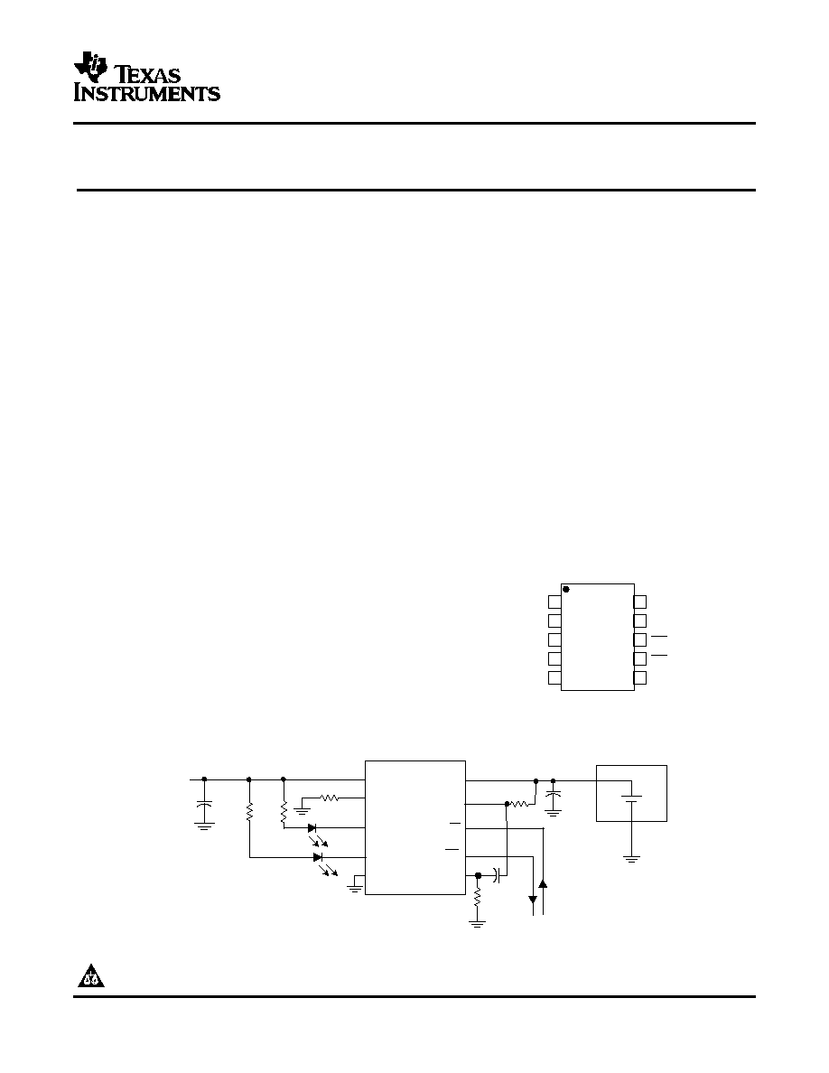
PINOUT
APPLICATIONS
IN
STAT1
CE
6
STAT2
V
SS
ISET
PG
TMR
BAT
bq24061/66
10
9
8
7
5
1
2
3
4
OUT
TYPICAL APPLICATION CIRCUIT
IN
STAT1
CE
OUT
STAT2
ISET
PG
RSET
TMR
R
1
2
3
4
5
6
7
8
9
10
BAT
Input Power
V
SS
4.7 F
m
1.5 kW 1.5 kW
1.13 kW
4.7 F
m
49.9 kW
+
Pack-
Pack+
Charge Enable and
Input Power Status
Li-lon or Li-Pol
Battery Pack
bq24061/66
0.47 F
m
TMR
R
BAT
200
bq2406x
SLUS689 JUNE 2006
1A SINGLE-CHIP Li-Ion/Li-Pol CHARGE MANAGEMENT IC
WITH THERMAL REGULATION
·
Thermal Regulation Maximizes Charge Rate
The bq2406x series are highly integrated Li-Ion and
Li-Pol linear chargers, targeted at space-limited
·
Ideal for Low-Dropout Designs for Single-Cell
portable applications. The bq2406x series offers a
Li-Ion or Li-Pol Packs in Space Limited
variety of safety features and functional options,
Applications
while still implementing a complete charging system
·
Integrated Power FET and Current Sensor for
in a small package. The battery is charged in three
up to 1-A Charge Applications
phases: conditioning, constant or thermally regulated
·
Reverse Leakage Protection Prevents Battery
current, and constant voltage. Charge is terminated
based
on
minimum
current.
An
internal
Drainage
programmable charge timer provides a backup
·
±
0.5% Voltage Regulation Accuracy
safety
feature
for
charge
termination
and
is
·
Charge Termination by Minimum Current and
dynamically adjusted during the thermal regulation
Time
phase. The bq2406x automatically re-starts the
charge if the battery voltage falls below an internal
·
Precharge Conditioning With Safety Timer
threshold; sleep mode is set when the external input
·
Status Outputs for LED or System Interface
supply is removed. Multiple versions of this device
Indicate Charge, Fault, and Power Good
family enable easy design of the bq2406x in cradle
Outputs
chargers or in the end equipment, while using low
·
Short-Circuit and Thermal Protection
cost or high-end AC adapters.
·
Automatic Sleep Mode for Low Power
Consumption
(TOP VIEW)
·
Small 3
×
3 mm MLP Package
·
Selectable Battery Insertion and Battery
Absent Detection
·
Input Over-Voltage Protection
·
PDA, MP3 Players, Digital Cameras
·
Internet Appliances and Handheld Devices
Please be aware that an important notice concerning availability, standard warranty, and use in critical applications of Texas
Instruments semiconductor products and disclaimers thereto appears at the end of this data sheet.
UNLESS
OTHERWISE
NOTED
this
document
contains
Copyright © 2006, Texas Instruments Incorporated
PRODUCTION DATA information current as of publication date.
Products conform to specifications per the terms of Texas
Instruments standard warranty. Production processing does not
necessarily include testing of all parameters.

www.ti.com
ABSOLUTE MAXIMUM RATINGS
(1)
RECOMMENDED OPERATING CONDITIONS
DISSIPATION RATINGS
(1)
bq2406x
SLUS689 JUNE 2006
AVAILABLE OPTIONS
Charge Input Over
Termination
Safety
Power
IC
Pack
Pack Voltage
Devices
(1) (2)
Marking
Voltage
Voltage
Enable
Timer
Good
Enable
Temp
Detection
Enable
Status
(Absent)
4.2 V
6.5 V
TMR pin
TMR pin
PG pin
No
TS pin
With timer
bq24060
BPG
enabled
4.2 V
6.5 V
TMR pin
TMR pin
PG pin
CE pin
No
With timer
bq24061
BPH
enabled
4.2 V
6.5 V
TE pin
TMR pin
No
CE pin
No
With termination
bq24063
Preview
enabled
4.2 V
10.5 V
TMR pin
TMR pin
PG pin
No
TS pin
With timer
bq24064
BSA
enabled
(1)
The bq2406x are only available taped and reeled. Add suffix R to the part number for quantities of 3,000 devices per reel (e.g.,
bq24060BPGR). Add suffix T to the part number for quantities of 250 devices per reel (e.g., bq24060DRCT).
(2)
This product is RoHS compatible, including a lead concentration that does not exceed 0.1% of total product weight, and is suitable for
use in specified lead-free soldering processes. In addition, this product uses package materials that do not contain halogens, including
bromine (Br) or antimony (Sb) above 0.1% of total product weight.
bq2406x
Supply voltage (IN with respect to Vss)
0.3 V to 18 V
(2)
Input voltage on IN, STATx, PG, TS, CE, TE, TMR (all with respect to Vss)
0.3 V to V(IN)
Input voltage on OUT, BAT, ISET (all with respect to Vss)
0.3 V to 7 V
Output sink current (STATx) + PG
15 mA
Output current (OUT pins)
1.5 A
T
A
Operating free-air temperature range
40
°
C to 125
°
C
T
stg
Storage temperature range
65
°
C to 150
°
C
T
J
Junction temperature range
40
°
C to 150
°
C
Lead temperature (Soldering, 10 sec)
300
°
C
(1)
Stresses beyond those listed under absolute maximum ratings may cause permanent damage to the device. These are stress ratings
only, and functional operation of the device at these or any other conditions beyond those indicated under recommended operating
conditions is not implied. Exposure to absolutemaximumrated conditions for extended periods may affect device reliability
(2)
The bq2406x device can withstand up to 26 V for a maximum of 87 hours.
MIN
TYP
MAX
UNIT
V
(IN)
Supply voltage range
Battery absent detection not functional
3.5
16.5
V
V
(IN)
Supply voltage range
Battery absent detection functional
4.35
16.5
V
T
J
Junction temperature
0
125
°
C
PACKAGE
JC
(
°
C/W)
JA
(
°
C/W)
10-pin DRC
3.21
46.87
(1)
This data is based on using the JEDEC High-K board and the exposed die pad is connected to a Cu
pad on the board. This is connected to the ground plane by a 2×3 via matrix.
2
Submit Documentation Feedback
www.ti.com
ELECTRICAL CHARACTERISTICS
bq2406x
SLUS689 JUNE 2006
over recommended operating, T
J
: 0 125
°
C range, See the Application Circuits section, typical values at T
J
: 25
°
C (unless
otherwise noted)
PARAMETER
TEST CONDITIONS
MIN
TYP
MAX
UNIT
POWER-ON-RESET
V(IN) = 0 V, increase V(OUT): 0
3 V OR
V
(PDWN)
Power down threshold
V(OUT) = 0 V, increase V(IN): 0
3 V,
1.5
3.0
V
CE = LO
(1)
INPUT POWER DETECTION, CE = HI or LOW, V(IN) > 3.5 V
V
IN(DT)
Input power detection threshold
V
(IN)
detected at [V(IN) V(OUT)] > V
IN(DT)
130
mV
Input power not detected at
V
HYS(INDT)
Input power detection hysteresis
30
mV
[V
(IN)
V
(OUT)]
< [V
IN(DT)
V
HYS(INDT)
]
Deglitch time, input power detected
PG:HI
LO, Thermal regulation loop not active,
T
DGL(INDT1)
1.5
3.5
ms
status
R
TMR
= 50 K
or V
(TMR)
= OPEN
Delay time, input power not detected
T
DGL(NOIN)
PG: LO
HI after T
DGL(NOIN)
10
µ
s
status
Charger turned off after T
DLY(CHGOFF)
, Measured from
T
DLY(CHGOFF)
Charger off delay
28
32
ms
PG: LO
HI; Timer reset after T
DLY(CHGOFF)
INPUT OVER-VOLTAGE PROTECTION
bq24060/61/63/65/66
6.2
6.5
7.0
Input over-voltage detection
V
(OVP)
V(IN) increasing
V
threshold
bq24064
10.2
10.5
11.7
bq24060/61/63/65/66
0.1
0.2
V
HYS(OVP)
Input over-voltage hysteresis
V(IN) decreasing
V
bq24064
0.3
0.5
CE = HI or LO, Measured from V(IN) > V
(OVP)
to
T
DGL(OVDET)
Input over-voltage detection delay
10
100
µ
s
PG: LO
HI; VIN increasing
Input over-voltage not detected
CE = HI or LO, Measured from V(IN) < V
(OVP)
T
DGL(OVNDET)
10
100
µ
s
delay
to PG: HI
LO; V(IN) decreasing
QUIESCENT CURRENT
V
(IN)
= 6 V
100
200
Input power detected,
I
CC(CHGOFF)
IN pin quiescent current, charger off
µ
A
CE = HI
V
(IN)
= 16.5 V
300
I
CC(CHGON)
IN pin quiescent current, charger on
Input power detected, CE = LO, V
BAT
= 4.5 V
4
6
mA
Battery leakage current after
Input power detected, charge terminated,
I
BAT(DONE)
1
5
µ
A
termination into IC
CE = LO
Battery leakage current into IC,
Input power detected, CE = HI OR
I
BAT(CHGOFF)
1
5
µ
A
charger off
input power not detected, CE = LO
TS PIN COMPARATOR
Lower voltage temperature
V
(TS1)
Hot detected at V(TS) < V
(TS1)
; NTC thermistor
29
30
31
%V(IN)
threshold
Upper voltage temperature
V
(TS2)
Cold detected at V(TS) > V
(TS2)
; NTC thermistor
60
61
62
%V(IN)
threshold
Temp OK at V(TS) > [ V
(TS1)
+ V
HYS(TS)
] OR
V
HYS(TS)
Hysteresis
2
%V(IN)
V
(TS)
< [ V
(TS2)
V
HYS(TS)
]
CE INPUT
V
IL
Input (low) voltage
V(CE) increasing
0
1
V
V
IH
Input (high) voltage
V(CE) decreasing
2.0
V
STAT1, STAT2 AND PG OUTPUTS , V(IN)
V
O(REG)
+ V
(DO-MAX)
V
OL
Output (low) saturation voltage
Ioutput = 5 mA (sink)
0.5
V
THERMAL SHUTDOWN
T
(SHUT)
Temperature trip
Junction temperature
155
°
C
T
(SHUTHYS)
Thermal hysteresis
Junction temperature
20
°
C
(1)
Specified by design, not production tested.
3
Submit Documentation Feedback
www.ti.com
ELECTRICAL CHARACTERISTICS (Continued)
mA
k
W
Volts
bq2406x
SLUS689 JUNE 2006
over recommended operating, T
J
: 0125
°
C range, See the Application Circuits section, typical values at T
J
: 25
°
C (unless
otherwise noted)
PARAMETER
TEST CONDITIONS
MIN
TYP
MAX
UNIT
VOLTAGE REGULATION, V(IN)
V
O(REG)
+ V
(DO-MAX)
, I
(TERM)
< I
(OUT)
< I
O(OUT)
, CHARGER ENABLED, NO FAULT CONDITIONS
DETECTED
bq24060/61/62/63/64
4.20
V
O(REG)
Output voltage
V
bq24065/66 versions only
4.36
T
A
= 25
°
C
0.5%
0.5%
V
O(TOL)
Voltage regulation accuracy
1%
1%
V
(DO)
Dropout voltage, V(IN) V(OUT)
I
(OUT)
= 1 A
750
mV
CURRENT REGULATION , V(IN) > V(OUT) > V
(DO-MAX)
, CHARGER ENABLED, NO FAULT CONDITIONS DETECTED
V
(BAT)
> V
(LOWV)
, I
O(OUT)
= I
(OUT)
= K
(SET)
×
I
O(OUT)
Output current range
100
1000
mA
V
(SET)
/R
SET
V
(SET)
Output current set voltage
V(ISET) = V
(SET)
, V
(LOWV)
< V(BAT)
V
O(REG)
2.45
2.50
2.55
V
100 mA
I
O(OUT)
1000 mA
315
335
355
K
(SET)
Output current set factor
10 mA
I
O(OUT)
< 100 mA
315
372
430
R
ISET
External resistor range
Resistor connected to ISET pin
0.7
10
k
VOLTAGE AND CURRENT REGULATION TIMING, V(IN) > V(OUT) + V
(DO-MAX)
, CHARGER ENABLED, NO FAULT CONDITIONS
DETECTED, R
TMR
= 50K or V(TMR) = OPEN; Thermal regulation loop not active
Input power detection to full
Measured from PG:HI
LO to I(OUT) > 100 mA,
T
PWRUP(CHG)
25
35
ms
charge current time delay
CE = LO, I
O(OUT)
= 1 A, V(BAT) = 3.5 V
Measured from CE:HI
LO to I(OUT) >100 mA,
Charge enable to full charge
T
PWRUP(EN)
I
O(OUT)
= 1A, V
(BAT)
= 3.5 V, V
(IN)
= 4.5 V, Input
25
35
ms
current delay
power detected
Measured from PG:HI
LO to V(OUT) > 90% of
Input power detection to voltage
charge voltage regulation;
T
PWRUP(LDO)
regulation delay, LDO mode set,
25
35
ms
V
(TMR)
= OPEN, LDO mode set, no battery and no
no battery or load connected
load at OUT pin, CE = LO
PRECHARGE AND OUTPUT SHORT-CIRCUIT CURRENT REGULATION, V(IN)V(OUT) > V(DO-MAX) , V(IN)
4.5V, CHARGER
ENABLED, NO FAULT CONDITIONS DETECTED, RTMR = 50K or V(TMR)=OPEN; Thermal regulation loop not active
Precharge to fast-charge transition
V
(LOWV)
V
(BAT)
increasing
2.8
2.95
3.15
V
threshold
V
(SCIND)
Short-circuit indication
V
(BAT)
decreasing
1.2
1.4
1.6
V
Precharge to short-circuit
V
(SC)
V
(BAT)
decreasing
1.6
1.8
2.0
transition threshold
V
(SC)
< V
I(BAT)
< V
(LOWV)
, t < T
(PRECHG)
I
O(PRECHG)
Precharge current range
10
100
mA
I
O(PRECHG)
= K
(SET)
×
V
(PRECHG
)/R
(ISET)
V
(ISET)
= V
(PRECHG)
,
V
(PRECHG)
Precharge set voltage
V
(SC)
< V
I(BAT)
< V
(LOWV)
,
225
250
280
mV
t < T
(PRECHG)
V
POR
< V
IN
< 6.0
15
22
30
V
I
O(SHORT)
Output shorted regulation current
I
O(SHORT)
= I
(OUT)
, V
(BAT)
= VSS
mA
6.0 V < V
IN
25
TEMPERATURE REGULATION (Thermal regulationTM), CHARGER ENABLED, NO FAULT CONDITIONS DETECTED
V(IN) = 5.5 V, V(BAT) = 3.2 V, Fast charge
T
J(REG)
Temperature regulation limit
101
112
125
°
C
current set to 1A
Minimum current in thermal
V(LOWV) < V(BAT) < VO(REG), 0.7k
< RISET
I
(MIN_TJ(REG))
200
250
mA
regulation
< 3.5k
4
Submit Documentation Feedback
www.ti.com
ELECTRICAL CHARACTERISTICS (Continued)
bq2406x
SLUS689 JUNE 2006
over recommended operating, T
J
: 0125
°
C range, See the Application Circuits section, typical values at T
J
: 25
°
C (unless
otherwise noted)
PARAMETER
TEST CONDITIONS
MIN
TYP
MAX
UNIT
CHARGE TERMINATION DETECTION, V
O(REG)
= 4.2 V or V
O(REG)
= 4.36 V, CHARGER ENABLED, NO FAULT CONDITIONS
DETECTED, Thermal regulation LOOP NOT ACTIVE, R
TMR
= 50K or TMR pin OPEN
Termination detection current
V
(BAT)
> V
(RCH)
, t < T
TDGL(TERM)
,
I
(TERM)
10
100
mA
range
I
(TERM)
= K
(SET)
×
V
(TERM)
/R
ISET
Charge termination detection
V
(TERM)
V
(BAT)
> V
(RCH)
225
250
275
mV
set voltage
Deglitch time, termination
T
DGL(TERM)
V
(ISET)
decreasing
15
25
35
ms
detected
BATTERY RECHARGE THRESHOLD
V
(RCH)
Recharge threshold detection
[V
O(REG)
V(BAT) ] > V
(RCH)
75
100
135
mV
Deglitch time, recharge
T
DGL(RCH)
V
(BAT)
decreasing
15
25
35
ms
detection
TIMERS, CE = LO, CHARGER ENABLED, NO FAULT CONDITIONS DETECTED, V(TMR) < 3 V, TIMERS ENABLED
T
(CHG)
Charge safety timer range
T
(CHG)
= K
(CHG)
×
R
TMR
; thermal loop not active
3
10
hours
K
(CHG)
Charge safety timer constant
V
(BAT)
> V
(LOWV)
0.08
0.1
0.12
hr/k
T
(PCHG)
= K
(PCHG)
×
T
(CHG)
×
K
(CHG)
; Thermal
T
(PCHG)
Pre-charge safety timer range
1080
3600
sec
regulation loop not active
Pre-charge safety timer
K
(PCHG)
V
(BAT)
< V
(LOWV)
0.08
0.1
0.12
constant
[Charge timer AND
Charge timer and termination
bq24060/61/62/64/
termination disabled] at V
(TMR)
enable threshold
65/66
> V
TMR(OFF)
V
TMR(OFF)
2.5
3.0
3.5
V
[Charge timer disabled] at
Charge timer enable threshold
bq24063
V
(TMR)
> V
TMR(OFF)
I
TMR(OFF)
= I
(TMR)
, V
(TMR)
= 3.5 V, V
(IN)
= 4.5 V,
I
TMR(OFF)
TMR pin pull-up current
1
6
µ
A
safety timer off, all other timers set to zero.
BATTERY DETECTION THRESHOLDS
I
DET(DOWN)
Battery detection current (sink)
2 V < V
(BAT)
< V
O(REG)
1
2
3.2
mA
Battery detection current
I
DET(UP)
2 V < V
(BAT)
< V
O(REG)
I
O(PRECHG)
mA
(source)
2 V < V
(BAT)
< V
O(REG)
, Thermal regulation loop not
T
(DETECT)
Battery detection time
active;
85
120
150
ms
R
TMR
= 50 k
TIMER FAULT RECOVERY
I
(FAULT)
Fault Current (source)
V
(OUT)
< V
(RCH)
12
10
8
mA
CHARGE OVER-CURRENT DETECTION, V(IN)
4.5 V, CHARGER ENABLED
Charge over-current detection
I
CH(OVC)
V
(ISET)
= VSS
2
A
threshold
Over current detection delay
Measured from V
(ISET)
= VSS to
T
DGL(CHOVC)
100
µ
s
time
I
O(OUT)
= 0
5
Submit Documentation Feedback
Document Outline