 | –≠–ª–µ–∫—Ç—Ä–æ–Ω–Ω—ã–π –∫–æ–º–ø–æ–Ω–µ–Ω—Ç: BQ24205 | –°–∫–∞—á–∞—Ç—å:  PDF PDF  ZIP ZIP |
bq24200, bq24201, bq24202
bq24203, bq24204, bq24205
SLUS501A ≠ OCTOBER 2001
SINGLE CHIP LI ION AND LI POL CHARGE MANAGEMENT IC
FOR CURRENT LIMITED APPLICATIONS
1
www.ti.com
FEATURES
D
Designed Specifically to Work With
Current-Limited Wall Supplies
D
Ideal for Low Dropout Charger Design for
Single-Cell Li-Ion Packs With Coke or
Graphite Anodes
D
Integrated PowerFET for 500 mA
D
Integrated Voltage Regulation With 0.5%
Accuracy
D
Battery Insertion and Removal Detection
D
Charge Termination by Minimum Current and
Time
D
Pre-Charge Conditioning With Safety Timer
D
Sleep Mode for Low-Power Consumption
D
Charge Status Output for LED or Host
Processor Interface Indicates
Charge-in-Progress, Charge Completion, and
Fault Conditions
D
Optional Temperature Monitoring Before and
During Charge
D
Small, 8-Pin Power-Pad MSOP Package
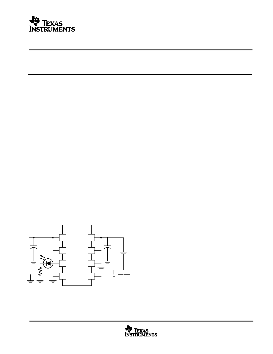
TYPICAL APPLICATION
DESCRIPTION
The bq2420x series are simple Li-Ion linear
charge management devices targeted at low-cost
and space limited charger applications. The
bq2420x series offer integrated powerFET,
high-accuracy voltage regulation, temperature
monitoring, charge status, and charge
termination, in a single monolithic device.
The bq2420x is designed to work with a
current-limited wall-mount transformer and
therefore does not provide any current regulation.
However, these devices offer a fixed internal
current limit to prevent damage to the internal
powerFET. A time-limited pre-conditioning phase
is provided to condition deeply discharged cells.
Once the battery reaches the charge voltage, the
high accuracy voltage regulation loop takes over
and completes the charge cycle. Charge is
terminated based on minimum current. An internal
charge timer provides a backup safety for charge
termination.
Other standard features include an automatic
sleep mode activated when V
CC
falls below the
battery voltage and a recharge feature activated
when the battery voltage falls below the V
RCH
threshold.
In addition to the standard features, the core
product provides two additional enhancements:
temperature monitoring and status display. The
temperature-sense circuit continuously measures
battery temperature using an external thermistor
and inhibits charge until the battery temperature is
within the user≠defined thresholds. The STAT pin
indicates three conditions of operation of the
charger. These conditions are charge-
in-progress, charge complete, and fault. This
output can be used to drive an LED or an interface
to a microcontroller.
Copyright
2001, Texas Instruments Incorporated
1
4
2
8
IN
VCC
VSS
OUT
7
BAT
6
CE
5
N/C
C1
bq24202DGN
3
STAT
DC+
DC≠
R1
C1
+
BATTERY PACK
UDG≠01111
PRODUCTION DATA information is current as of publication date.
Products conform to specifications per the terms of Texas Instruments
standard warranty. Production processing does not necessarily include
testing of all parameters.
bq24200, bq24201, bq24202
bq24203, bq24204, bq24205
SLUS501A ≠ OCTOBER 2001
2
www.ti.com
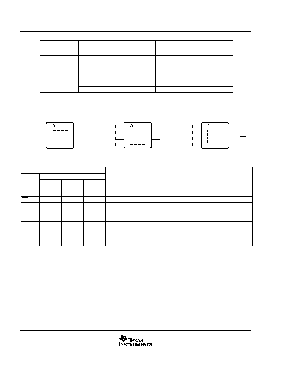
AVAILABLE OPTIONS
TJ
CHARGE
REGULATION
VOLTAGE
OPTIONAL
FUNCTIONS
MARKING
PACKAGED
DEVICES
(DGN)
4.2 V
STAT and TS
AZC
bq24200DGN
4.1 V
STAT and TS
AZD
bq24201DGN
40
_
C to 125
_
C
4.2 V
STAT
AZE
bq24202DGN
≠40
_
C to 125
_
C
4.1 V
STAT
AZF
bq24203DGN
4.2 V
≠
AZG
bq24204DGN
4.1 V
≠
AZI
bq24205DGN
The DGN package is available taped and reeled. Add TR suffix to device type (e.g. bq24200DGNTR) to order. Quantities
2500 devices per reel.
OUT
BAT
CE
N/C
8
7
6
5
1
2
3
4
IN
V
CC
N/C
V
SS
bq24200, bq24201
HTSSOP (DGN) PACKAGE
(TOP VIEW)
OUT
BAT
TS
N/C
8
7
6
5
1
2
3
4
IN
V
CC
STAT
V
SS
OUT
BAT
CE
N/C
8
7
6
5
1
2
3
4
IN
V
CC
STAT
V
SS
bq24202, bq24203
HTSSOP (DGN) PACKAGE
(TOP VIEW)
bq24204, bq24205
HTSSOP (DGN) PACKAGE
(TOP VIEW)
*
*
*
* Thermal pad is electrically connected to the ground of the device (VSS).
Terminal Functions
TERMINAL
NO.
I/O
DESCRIPTION
NAME
bq24200
bq24201
bq24202
bq24203
bq24204
bq24205
I/O
DESCRIPTION
BAT
7
7
7
I
Battery voltage sense input
CE
≠
6
6
I
Charge enable Input (active low)
IN
1
1
1
I
Charge input voltage
N/C
5
5
3, 5
≠
No connection. Must be left floating
OUT
8
8
8
O
Charge current output
STAT
3
3
≠
O
Charge status output
TS
6
≠
≠
I
Temperature sense input
VCC
2
2
2
I
VCC input
VSS
4
4
4
≠
Ground input
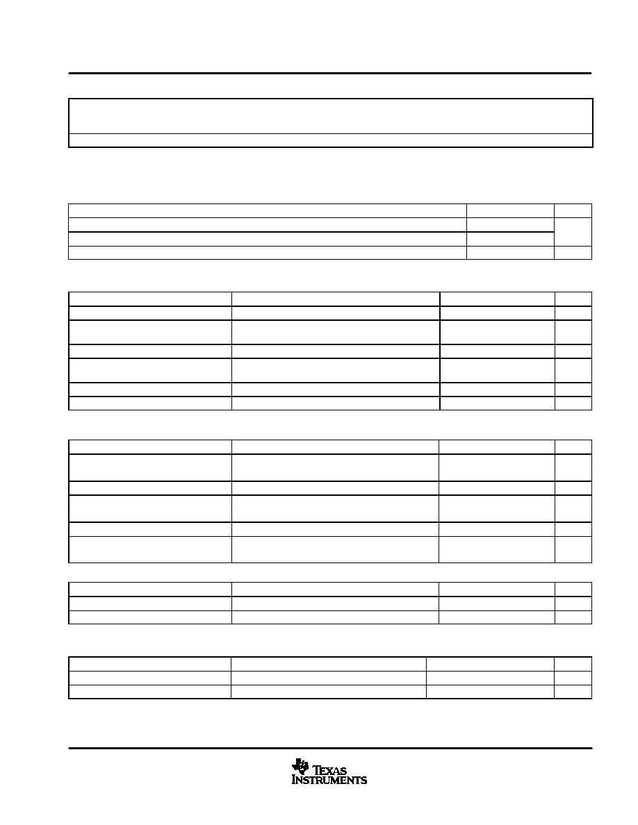
absolute maximum ratings over operating free≠air temperature range (unless otherwise noted)
Supply voltage (Vcc with respect to GND)
16.5 V
. . . . . . . . . . . . . . . . . . . . . . . . . . . . . . . . . . . . . . . . . . . . . . . . . . .
Input voltage, IN, STAT, TS (all with respect to GND)
16.5 V
. . . . . . . . . . . . . . . . . . . . . . . . . . . . . . . . . . . . . . . . . .
Input voltage, BAT, OUT (all with respect to GND)
7 V
. . . . . . . . . . . . . . . . . . . . . . . . . . . . . . . . . . . . . . . . . . . . . . .
Output sink/source current (STAT)
15 mA
. . . . . . . . . . . . . . . . . . . . . . . . . . . . . . . . . . . . . . . . . . . . . . . . . . . . . . . . .
Storage temperature range, T
stg
≠65
_
C to 150
_
C
. . . . . . . . . . . . . . . . . . . . . . . . . . . . . . . . . . . . . . . . . . . . . . . . . . .
Junction temperature range, T
J
≠40
_
C to 125
_
C
. . . . . . . . . . . . . . . . . . . . . . . . . . . . . . . . . . . . . . . . . . . . . . . . . . . .
Lead temperature (soldering, 10sec)
300
_
C
. . . . . . . . . . . . . . . . . . . . . . . . . . . . . . . . . . . . . . . . . . . . . . . . . . . . . . . .
Stresses beyond those listed under "absolute maximum ratings" may cause permanent damage to the device. These are stress ratings only, and
functional operation of the device at these or any other conditions beyond those indicated under "recommended operating conditions" is not
implied. Exposure to absolute≠maximum≠rated conditions for extended periods may affect device reliability.
bq24200, bq24201, bq24202
bq24203, bq24204, bq24205
SLUS501A ≠ OCTOBER 2001
3
www.ti.com
dissipation ratings
PACKAGE
THERMAL IMPEDANCE
JUNCTION-TO-AMBIENT
(
JA
THERMAL IMPEDANCE
JUNCTION-TO-CASE
(
JC
TA 25
∞
C
POWER
RATING
DERATING FACTOR
ABOVE
TA = 25
∞
C
8 Pin DGN (1)
57.20
∞
C/W
4.4
∞
C/W
1.75 W
0.017 W/
∞
C
NOTE 1: This data is based on using JEDEC High-K board and topside traces, top and bottom thermal pad (2mm
◊
3mm), internal 1 oz. power
and ground planes, four thermal via underneath the die connecting to ground plane.
recommended operating conditions
MIN
MAX
UNIT
Supply voltage, VCC
V(LOWV≠MIN)
13.5
V
Input voltage, VIN
V(LOWV≠MIN)
13.5
V
Operating junction temperature range, TJ
≠40
125
∞
C
electrical characteristics over 0
∞
C
T
J
125
∞
C and supply voltage range
(unless otherwise noted)
PARAMETER
TEST CONDITIONS
MIN
TYP
MAX
UNIT
Vcc Current, ICC(VCC)
Vcc > Vcc(min)
1.7
2.5
mA
Sleep current , ICC(SLP)
Sum of currents into OUT and BAT pins, Vcc<V(SLP),
0oC
Tj
85oC
5
µ
A
Sleep current , ICC(SLP)
Sum of currents into OUT and BAT pins, Vcc<V(SLP)
10
µ
A
Standby Current, ICC(STDBY)
Sum of currents into Vcc, IN and TS pins,
(Vcc≠VI(TS))
300 mV
1
mA
Input Bias Current on BAT pin, IIB (BAT)
1
µ
A
Input Bias Current on TS pin, IIB (TS)
0.1*Vcc
VI(TS)
0.8*Vcc
1
µ
A
voltage regulation, V
O(REG)
+ V
(DO≠MAX)
VCC, I
(TERM)
< I
O(OUT)
500 mA, over 0
∞
C
T
J
125
∞
C and supply
voltage range (unless otherwise noted)
PARAMETER
TEST CONDITIONS
MIN
TYP
MAX
UNIT
Output voltage, VO(REG)
VO(REG) + V(DO≠MAX)
10 V,
I(TERM) < IO(OUT)
250 mA
4.0795
4.10
4.1205
Volts
Output voltage, VO(REG)
4.05
4.10
4.15
Volts
Output voltage, VO(REG)
VO(REG) + V(DO≠MAX)
10 V,
I(TERM) < IO(OUT)
250 mA
4.1790
4.20
4.2210
Volts
Output voltage, VO(REG)
4.15
4.20
4.25
Volts
Dropout voltage (V(IN) ≠V(OUT)), V(DO)
VO(REG) + V(DO≠MAX)
Vcc,
IO(OUT) = 500 mA
200
350
500
mV
output current, over 0
∞
C
T
J
125
∞
C and supply voltage range (unless otherwise noted)
PARAMETER
TEST CONDITIONS
MIN
TYP
MAX
UNIT
Output current, IO(OUT)
See Note 1
500
mA
Short≠circuit Trip Current, I(SC)
See Note 1
1
1.6
A
NOTE 2: Assured by design, not production tested.
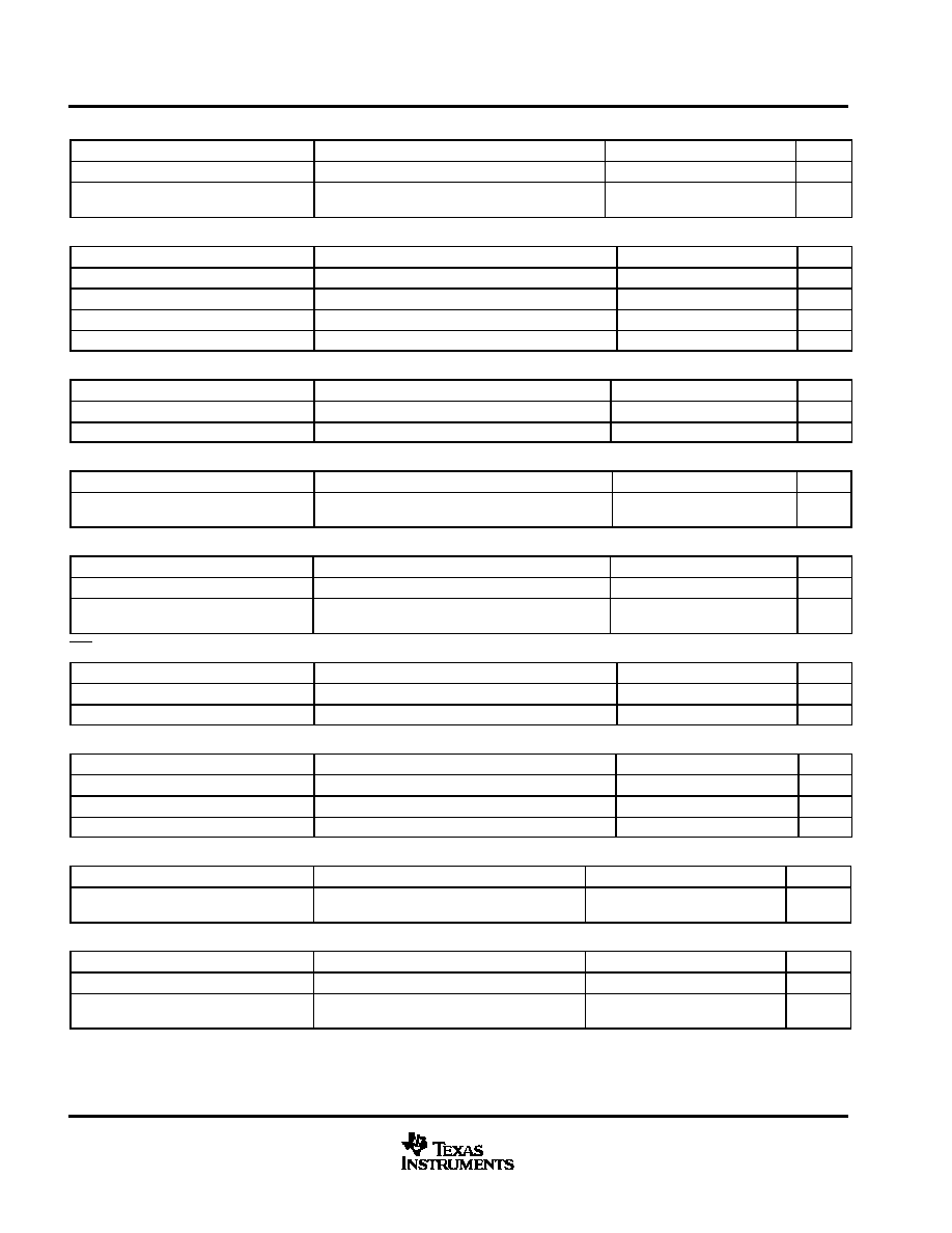
pre-charge current regulation, over 0
∞
C
T
J
125
∞
C and supply voltage range (unless otherwise noted)
PARAMETER
TEST CONDITIONS
MIN
TYP
MAX
UNIT
Pre≠charge Current , I(PRECHG)
VI(BAT) < V(LOWV),
t < t(30min)
10
13.5
17
mA
Battery Detection Current , I(DETECT)
VI(BAT) = 2.5 V,
t > t(30min)
160
210
300
µ
A
bq24200, bq24201, bq24202
bq24203, bq24204, bq24205
SLUS501A ≠ OCTOBER 2001
4
www.ti.com
charge termination detection, over 0
∞
C
T
J
125
∞
C And supply voltage range (unless otherwise noted)
PARAMETER
TEST CONDITIONS
MIN
TYP
MAX
UNIT
Taper current detect threshold, I(TAPER)
VI(BAT) > V(RCH)
22
25.5
29
mA
Charge termination current detect thresh-
old, I(TERM)
VI(BAT) > V(RCH)
0.8
1.1
1.4
mA
temperature comparator, over 0
∞
C
T
J
125
∞
C and supply voltage range (unless otherwise noted)
PARAMETER
TEST CONDITIONS
MIN
TYP
MAX
UNIT
Lower Temperature Threshold, V(TS1)
TS pin voltage
30
%VCC
Upper Temperature Threshold, V(TS2)
TS pin voltage
60
%VCC
Accuracy
≠0.7
0.7
%VCC
Hysteresis
1
%VCC
low voltage battery threshold, over 0
∞
C
T
J
125
∞
C and supply voltage range (unless otherwise noted)
PARAMETER
TEST CONDITIONS
MIN
TYP
MAX
UNIT
LowV Threshold, V(LOWV)
0oC
TJ
85oC
2.8
2.95
3.1
Volts
LowV Threshold, V(LOWV)
2.8
3.0
3.2
Volts
battery recharge threshold, over 0
∞
C
T
J
125
∞
C and supply voltage range (unless otherwise noted)
PARAMETER
TEST CONDITIONS
MIN
TYP
MAX
UNIT
Recharge Threshold, VRCH
VO(REG)
0.115
VO(REG)
≠0.1
VO(REG)
0.85
Volts
STAT output, Vcc
V
O(REG)
, over 0
∞
C
T
J
125
∞
C and supply voltage range (unless otherwise noted)
PARAMETER
TEST CONDITIONS
MIN
TYP
MAX
UNIT
Output (low) saturation voltage, VOL(STAT) Io = 10 mA
0.5
Volts
Output (high) saturation voltage
VOH(STAT)
Io = ≠5 mA
Vcc≠1.5
Volts
CE, over 0
∞
C
T
J
125
∞
C and supply voltage range (unless otherwise noted)
PARAMETER
TEST CONDITIONS
MIN
TYP
MAX
UNIT
Input (low) voltage, VIL(CE)
IIL = 5
µ
A
0
VCC≠1
Volts
Input (high) voltage VIH(CE)
IIH = 20
µ
A
Vcc≠0.3
Volts
timers, over 0
∞
C
T
J
125
∞
C and supply voltage range (unless otherwise noted)
PARAMETER
TEST CONDITIONS
MIN
TYP
MAX
UNIT
Pre-charge and taper timer, t(PRECHG)
1,548
2,065
2,581
sec
Taper timer, t(TAPER)
1,548
2,065
2,581
sec
Charge Timer, t(CHG)
9,292
12,389
15,486
sec
sleep comparator, over 0
∞
C
T
J
125
∞
C and supply voltage range (unless otherwise noted)
PARAMETER
TEST CONDITIONS
MIN
TYP
MAX
UNIT
Sleep≠mode threshold, V(SLP)
2.3V
VI(BAT)
VO(REG)
V(BAT)≠10
mV
Volts
power-on-reset and V
IN
Ramp Rate, over 0
∞
C
T
J
125
∞
C and supply voltage range (unless otherwise noted)
PARAMETER
TEST CONDITIONS
MIN
TYP
MAX
UNIT
POR Threshold, VPOR
See Note 1
2.3
2.4
2.5
Volts
Slew rate
See Note 1
5
5 x
10≠5
Volts/
µ
s
NOTE 1. Ensured by design, not production tested.
bq24200, bq24201, bq24202
bq24203, bq24204, bq24205
SLUS501A ≠ OCTOBER 2001
5
www.ti.com
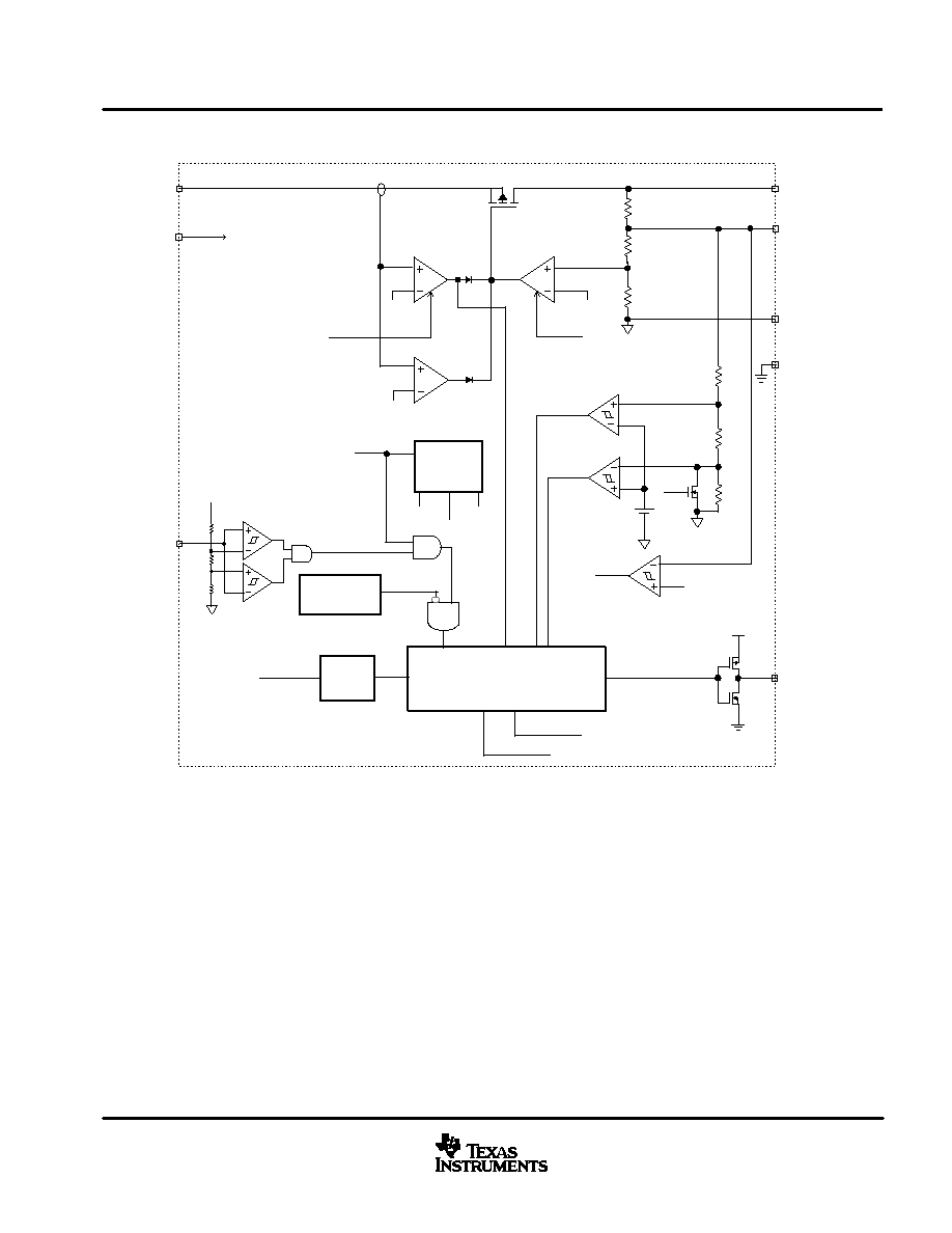
functional block diagram
UDG≠01105
BAT
VSS
ChargeOK
R1
R2
R4
R5
R6
PwrDwn*
IN
GND/HS
Vcc
LowV
VRCH
Vref
PwrDwn
*
Bias &
Ref
Generator
Vref
PwrDwn*
Charge Control,
Timer
and Display logic
ChargeOK
Pre-Charge ok
TS
Vref
Thermal
Shutdown
Suspend*
STAT
Vcc
OSC
PwrDwn
*
Pre-Charge ok
Iref
Vref
Iref
T
aperDet
Imax
Imax
Vcc
Vcc
OUT
R3
detailed description
IN: This pin is connected to the source of the internal P-channel powerFET.
OUT: This pin is connected to the drain of the internal P-channel powerFET.
Battery voltage sense (BAT): Voltage sense-input tied directly to the positive side of the battery.
Temperature sense input (TS): Input for an external battery-temperature monitoring circuit.
Charge status output (STAT): High-impedance indication of various charge conditions.
Supply voltage input (VCC): Power supply input