1
Features
ÿ
Safe management of fast charge
for NiCd and NiMH battery
packs.
ÿ
High-frequency switching con-
troller for efficient and simple
charger design
ÿ
Pre-charge qualification for
detecting shorted, damaged, or
overheated cells
ÿ
Fast-charge termination by
peak voltahge (PVD), maximum
temperature, and maximum
charge time
ÿ
Selectable top-off mode for
achieving maximum capacity in
NiMH batteries
ÿ
Programmable trickle-charge
mode for reviving deeply dis-
charged batteries and for post-
charge maintenance
ÿ
Built-in battery removal and in-
sertion detection
ÿ
Sleep mode for low power con-
sumption
General Description
The bq24400 is a programmable,
monolithic IC for fast-charge manage-
ment of nickel cadmium (NiCd) and
nickel metal-hydride (NiMH) batter-
ies.
The bq24400 provides a number of
charge termination criteria:
l
Peak voltage, PVD (for NiCd and
NiMH)
l
Maximum temperature
l
Maximum charge time
For safety, the bq24400 inhibits fast
charge until the battery voltage and
temperature are within user-defined
limits. If the battery voltage is below
the low-voltage threshold, the
bq24400 uses trickle-charge to
condition the battery. For NiMH
batteries, the bq24400 provides an
optional top-off charge to maximize
the battery capacity.
The integrated high-frequency com-
parator allows the bq24400 to be the
basis for a complete, high-efficiency
power-conversion circuit.
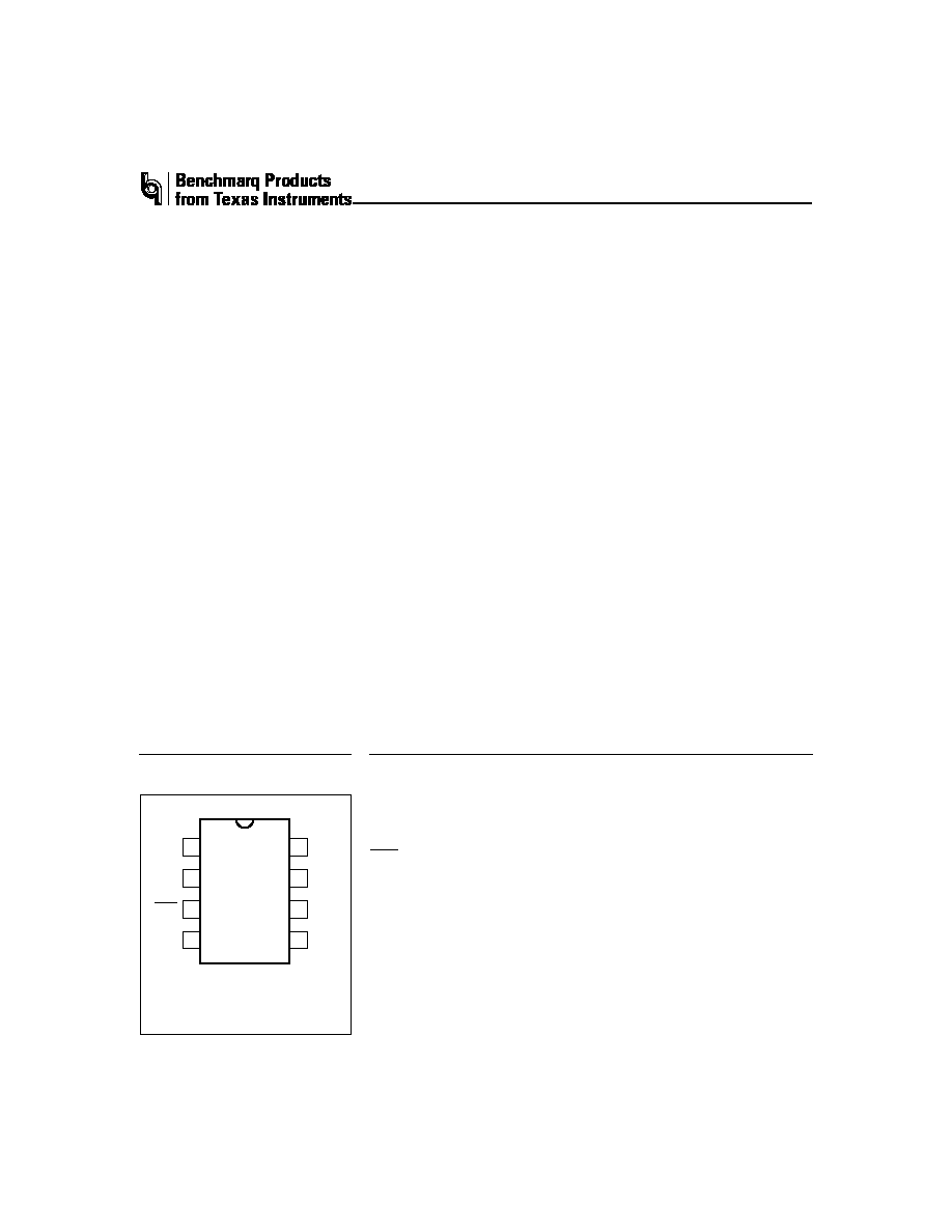
bq24400
SNS
Current-sense input
V
SS
System ground
LED
Charge-status
output
BAT
Battery-voltage
input
1
PN-2000.eps
8-Pin DIP or Narrow SOIC
or TSSOP
2
3
4
8
7
6
5
SNS
LED
BAT
VSS
MOD
VCC
TS
RC
Pin Connections
Pin Names
Programmable NiCd/NiMH
Fast-Charge Management Device
SLUS498 -SEPTEMBER 2001
TS
Temperature-sense
input
RC
Timer-program input
V
CC
Supply-voltage input
MOD
Modulation-control
output

Pin Descriptions
SNS
Current-sense input
Enables the bq24400 to sense the battery cur-
rent via the voltage developed on this pin by
an external sense-resistor connected in series
with the battery pack.
V
SS
System Ground
LED
Charge-status output
Open-drain output that indicates the charg-
ing status by turning on, turning off, or flash-
ing an external LED.
BAT
Battery-voltage input
Battery-voltage sense input. A simple resistive
divider, across the battery terminals, generates
this input.
TS
Temperature-sense input
Input for an external battery-temperature
monitoring circuit. An external resistive di-
vider network with a negative tempera-
ture-coefficient thermistor sets the lower and
upper temperature thresholds.
RC
Timer-program input
RC input used to program the maximum
charge-time, hold-off period, and trickle rate
during the charge cycle, and to disable or
enable top-off charge.
V
CC
Supply-voltage input
MOD
Modulation-control output
Push-pull output that controls the charging
current to the battery. MOD switches high to
enable charging current to flow and low to
inhibit charging- current flow.
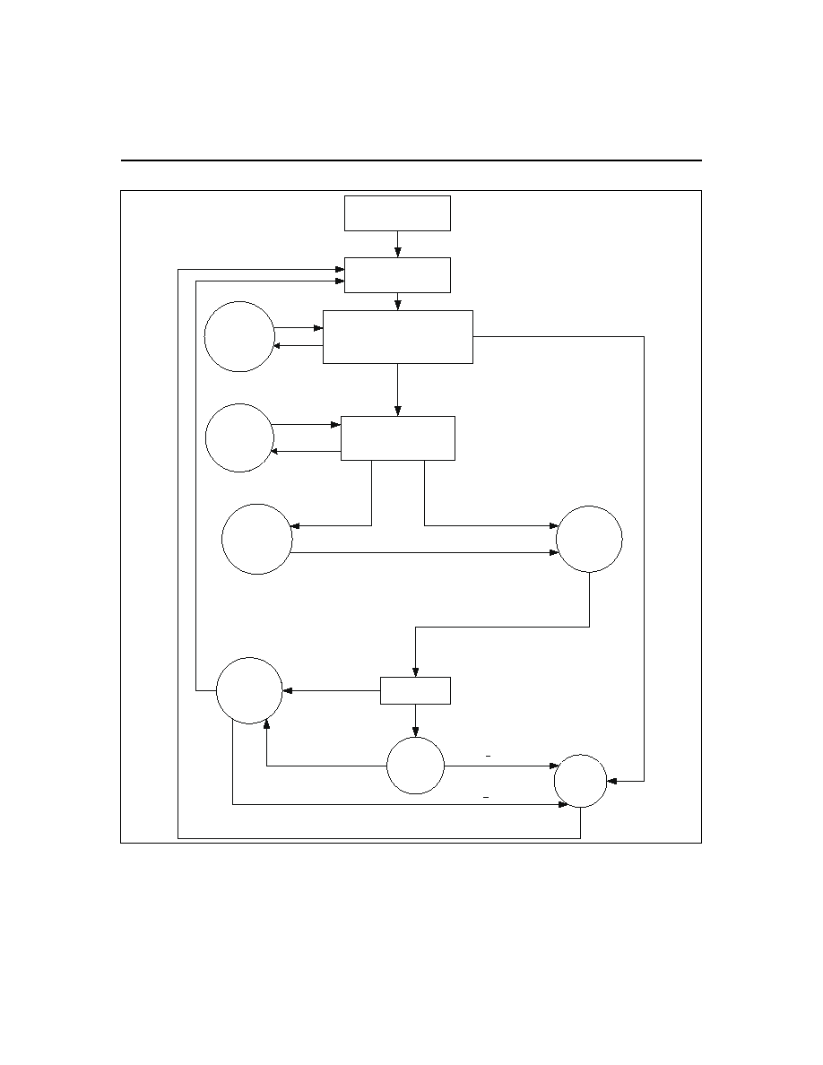
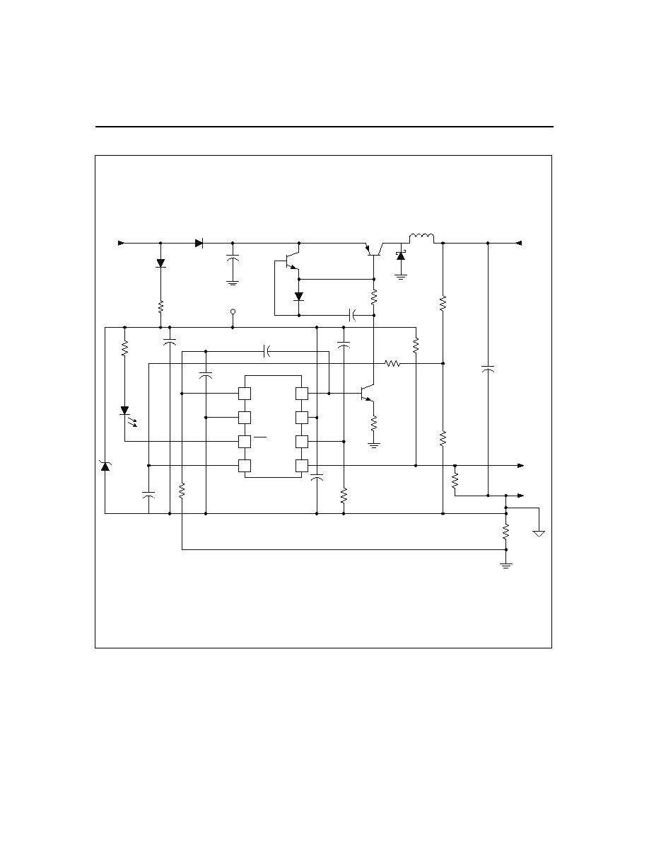
Functional Description
The bq24400 is a versatile, NiCd, NiMH battery- charge
control device. See Figure 1 for a functional block dia-
gram and Figure 2 for the state diagram.
2
bq24400
BD2000T.eps
Voltage
Reference
Internal
OSC
Clock
Phase
Generator
ADC
OSC
SNS
TS
MOD
RC
BAT
LED
V
CC
V
SS
Timer
T/
t
ALU
Voltage
Comparator
Voltage
Comparator
Charge
Control
Figure 1. Functional Block Diagram
3
bq24400
4.0 V <V
CC
<6.0 V
Battery Voltage
(PVD checked at rate
of MTO/64)
Sleep
Mode
Charge
Suspended
Charge
Initialization
Battery
Conditioning
Battery Temperature
(checked 1,750 times
per second)
V
BAT
<V
SLP
V
SLP
<V
BAT
<V
CC
V
BAT
<V
MCV
V
MCV
<V
BAT
<V
SLP
Current
Regulation
V
BAT
<V
LBAT
or
V
TS
>V
LTF
V
TS
>V
HTF
V
TS
<V
HTF
V
LBAT
<V
BAT
<V
MCV
and
V
HTF
<V
TS
<V
LTF
V
LBAT
<V
BAT
<V
MCV
and
V
HTF
<V
TS
<V
LTF
PVD (after hold-off period), or
V
TS
<V
TCO
or
Time =MTO
Top-Off
Selected?
Maintenance
Charge
No
Top-Off
Yes
Done
Time =MTO
or
V
TS
<V
TCO
V
BAT
>V
MCV
V
BAT
>V
MCV
V
CC
Reset or Battery Replacement
V
CC
Reset
Figure 2. State Diagram
UDG-01088

Initiation and Charge Qualification
The bq24400 initiates a charge cycle when it detects
l
Application of power to V
CC
l
Battery replacement
l
Exit from sleep mode
Immediately following initiation, the IC enters a
charge-qualification mode. The bq24400 charge qualifica-
tion is based on battery voltage and temperature. If
voltage on pin BAT is less than the internal threshold,
V
LBAT
, the bq24400 enters the charge-pending state.
This condition indicates the possiblility of a defective or
shorted battery pack. In an attempt to revive a fully
depleted pack, the bq24400 enables the MOD pin to
trickle-charge at a rate of once every 1.0s. As explained in
the section "Top-Off and Pulse-Trickle Charge," the
trickle pulse-width is user-selectable and is set by the
value of the resistance connected to pin RC.
During this period, the LED pin blinks at a 1Hz rate, in-
dicating the pending status of the charger.
Similarly, the bq24400 suspends fast charge if the battery
temperature is outside the V
LTF
to V
HTF
range. (See Table
4.) For safety reasons, however, it disables the pulse trickle,
in the case of a battery over-temperature condition (i.e., V
TS
< V
HTF
). Fast charge begins when the battery temperature
and voltage are valid.
NiCd and NiMH Batteries
Following qualification, the bq24400 fast-charges NiCd or
NiMH batteries using a current-limited algorithm. Dur-
ing the fast-charge period, it monitors charge time, tem-
perature, and voltage for adherence to the termination
criteria. This monitoring is further explained in later sec-
tions. Following fast charge, the battery is topped off, if
top-off is selected. The charging cycle ends with a trickle
maintenance-charge that continues as long as the voltage
on pin BAT remains below V
MCV
.
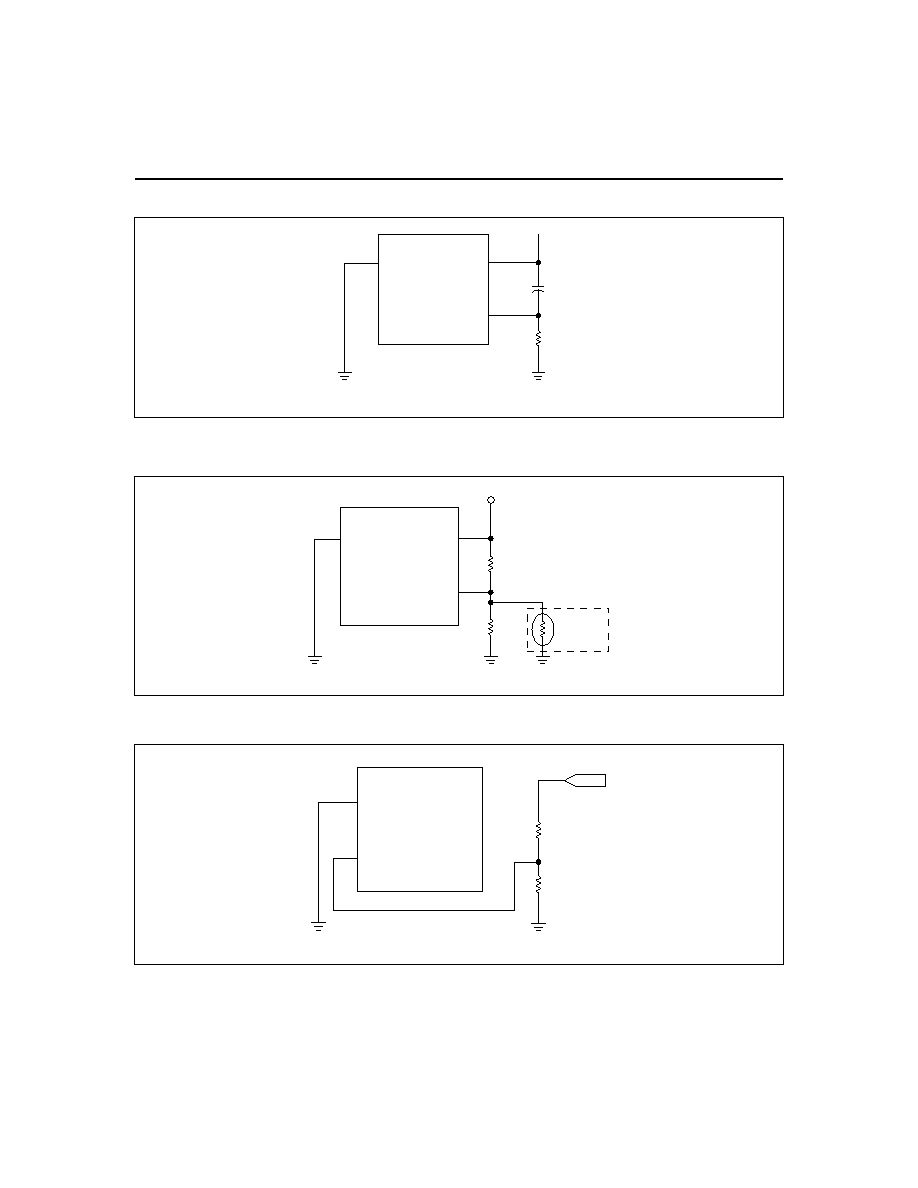
Charge Termination
Maximum Charge Time
The bq24400 sets the maximum charge-time through pin
RC. With the proper selection of external resistor and ca-
pacitor, various time-out values may be achieved. Figure
3 shows a typical connection.
The following equation shows the relationship between
the R
MTO
and C
MTO
values and the maximum charge
time (MTO) for the bq24400:
MTO = R
MTO
C
MTO
35,988
MTO is measured in minutes, R
MTO
in ohms, and C
MTO
in farads. (Note: R
MTO
and C
MTO
values also determine
other features of the device. See Tables 2 and 3 for de-
tails.)
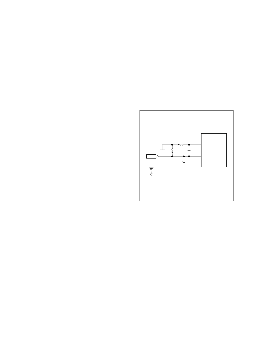
Maximum Temperature
A negative-coefficient thermistor, referenced to V
SS
and
placed in thermal contact with the battery, may be used
as a temperature-sensing device. Figure 4 shows a typical
temperature-sensing circuit.
During fast charge, the bq24400 compares the battery
temperature to an internal high-temperature cutoff
threshold, V
TCO
. As shown in Table 4, high-temperature
termination occurs when voltage at pin TS is less than
this threshold.
Peak Voltage
The bq24400 uses a peak-voltage detection (PVD) scheme
to terminate fast charge for NiCd and NiMH batteries.
The bq24400 continuously samples the voltage on the
BAT pin, representing the battery voltage, and triggers
the peak detection feature if this value falls below the
maximum sampled value by as much as 3.8 mV (PVD).
As shown in figure 5, a resistor voltage-divider between
the battery pack's positive terminal and V
SS
scales the
battery voltage measured at pin BAT.
The resistor values R
B1
And R
B2
are calculated by the fol-
lowing equation:
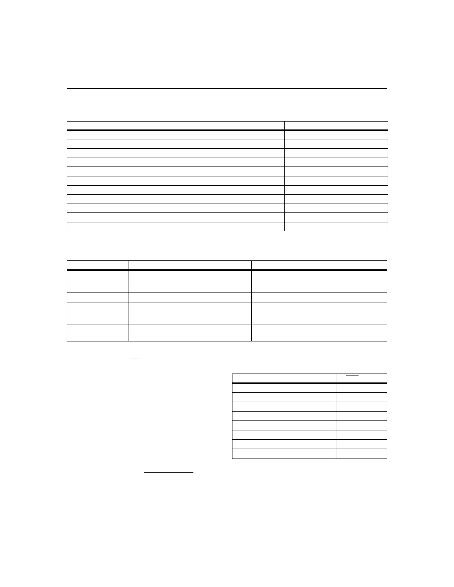
4
bq24400
Battery Chemistry
Charge Algorithm
NiCd or NiMH
1. Charge qualification
2. Trickle charge, if required
3. Fast charge (constant current)
4. Charge termination (
T/
t, time)
5. Top-off (optional)
6. Trickle charge
Table 1. Charge Algorithm
5
bq24400
F2000T RCI.eps
bq2000T
2
V
CC
RC
7
6
C
MTO
R
MTO
V
SS
Figure 3. Typical Connection for the RC Input
F2000TTMC.eps
bq2000T
2
7
Battery
Pack
5
R
T2
R
T1
V
SS
V
CC
V
CC
TS
N
T
C
Figure 4. Temperature Monitoring Configuration
F2000TBVD.eps
BAT+
bq2000T
2
4
R
B1
R
B2
V
SS
BAT
Figure 5. Battery Voltage Divider
bq24400
bq24400
bq24400
R
R
N 1
B1
B2
=
-
where N is the number of cells in series.
The end-to-end input impedance of this resistive divider
network should be at least 200kW and no more than
1MW.
Initial Hold-Off Period
The values of the external resistor and capacitor con-
nected to pin RC set the initial hold-off period. During
this period, the bq24400 avoids early termination by dis-
abling the
T/
t feature. This period is fixed at the pro-
grammed value of the maximum charge time divided by
32.
hold-off period =
maximum time - out
32
Top-Off and Pulse-Trickle Charge
6
bq24400
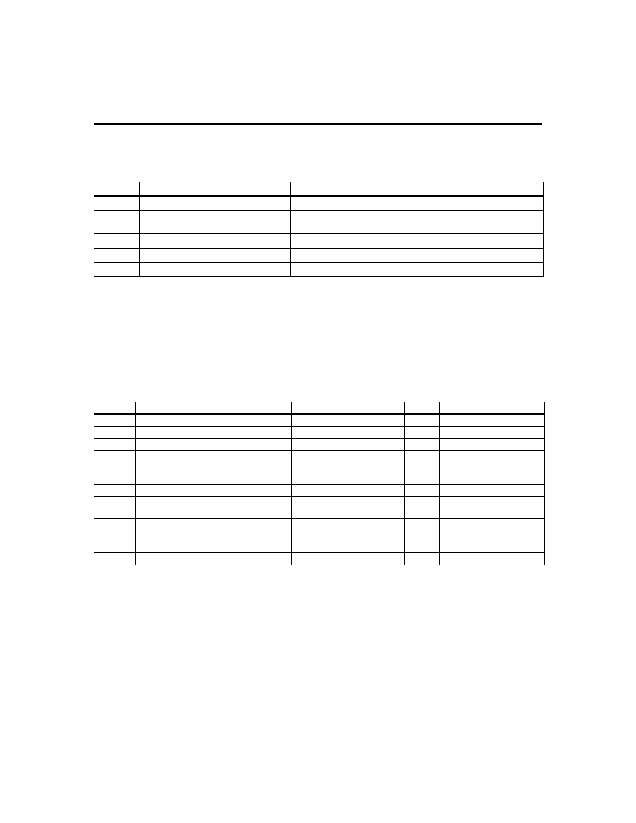
Parameter
Value
Maximum cell voltage (V
MCV
)
2V
Minimum pre-charge qualification voltage (V
LBAT
)
950mV
High-temperature cutoff voltage (V
TCO
)
0.225
V
CC
High-temperature fault voltage (V
HTF
)
0.25
V
CC
Low-temperature fault voltage (V
LTF
)
0.5
V
CC
bq24400 fast-charge maximum time out (MTO)
R
MTO
C
MTO
35,988
Fast-charge charging current (I
MAX
)
0.05/R
SNS
Hold-off period
MTO/32
Top-off charging current (optional)
I
MAX
/16
Top-off period (optional)
MTO
Trickle-charge frequency
1Hz
Table 2. Summary of NiCd or NiMH Charging Characteristics
Temperature
Condition
Action
V
TS
> V
LTF
Cold battery--checked at all times
Suspends fast charge or top-off and timer
Allows trickle charge--LED flashes at 1Hz rate
during pre-charge qualification and fast charge
V
HTF
< V
TS
< V
LTF
Optimal operating range
Allows charging
V
TS
< V
HTF
Hot battery--checked during charge qualifi-
cation and top-off and trickle-charge
Suspends fast-charge initiation, does not allow
trickle charge--LED flashes at 1Hz rate during
pre-charge qualification
V
TS
< V
TCO
Battery exceeding maximum allowable tem-
perature--checked at all times
Terminates fast charge or top-off
Table 3. Temperature-Monitoring Conditions
Table 4. Charge Status Display
Charge Action State
LEDStatus
Battery absent
High impedance
Pre-charge qualification
1Hz flash
Trickle charge (before fast charge)
1Hz flash
Fast charging
Low
Top-off or trickle
High impedance
Charge complete
High impedance
Sleep mode
High impedance
Charge suspended (V
TS
> V
LTF
)
1Hz flash
Top-off may be desirable on batteries that have a ten-
dency to terminate charge before reaching full capacity.
To enable this option, the capacitance value of C
MTO
con-
nected to pin RC (Figure 3) should be greater than
0.13
µ
F, and the value of the resistor connected to this pin
should be less than 15k
. To disable top-off, the capaci-
tance value should be less than 0.07
µ
F. The tolerance of
the capacitor needs to be taken into account in compo-
nent selection.
Once enabled, the top-off is performed over a period
equal to the maximum charge time at a rate of
1
16
that of
fast charge.
Following top-off, the bq24400 trickle-charges the battery
by enabling the MOD to charge at a rate of once every 1.0
second. The trickle pulse-width is user-selectable and is
set by the value of the resistor R
MTO
, which is on pin RC.
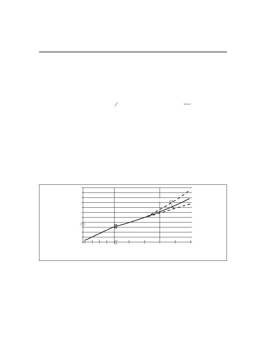
Figure 6 shows the relationship between the trickle
pulse-width and the value of R
MTO
. The typical tolerance
of the pulsewidth below 150k
is
±
10%.
During top-off and trickle-charge, the bq24400 monitors
battery voltage and temperature. These functions are
suspended if the battery voltage rises above the
maximum cell voltage (V
MCV
) or if the temperature
exceeds the high-temperature fault threshold (V
HTF
).
Charge Current Control
The bq24400 controls the charge current through the
MOD output pin. The current-control circuit supports a
switching-current regulator with frequencies up to
500kHz. The bq24400 monitors charge current at the
SNS input by the voltage drop across a sense-resistor,
R
SNS
, in series with the battery pack. See Figure 8 for a
typical current-sensing circuit. R
SNS
is sized to provide
the desired fast-charge current (I
MAX
):
I
MAX
=
0.05
R
SNS
If the voltage at the SNS pin is greater than V
SNSLO
or
less than V
SNSHI
, the bq24400 switches the MOD output
high to pass charge current to the battery. When the SNS
voltage is less than V
SNSLO
or greater than V
SNSHI
, the
bq24400 switches the MOD output low to shut off
charging current to the battery. Figure 7 shows a typical
multi-chemistry charge circuit.
7
bq24400
1
2
4
6
8
10
50
100
150
200
250
2
3
4
20
40
60
Pulse
width--ms
R
MTO
--k
80
100
120
140
160
2000PNvB3.eps
Shows Tolerance
Figure 6. Relationship Between Trickle Pulse-Width and Value of R
MTO
8
bq24400
1
2
3
4
8
7
6
5
C4
0.0022 mF
R1
100kW
C7
4.7 PF
C2
0.1 mF
C3
10 mF
R13
1.1 kW
R8
6.81 kW
SNS
VSS
LED
BAT
TS
RC
VCC
MOD
BQ24401
C1
0.1 mF
V
CC
D1
RED
R4
12.4 kW
C8
0.33 mF
R5
20 kW
R11
220 W
R12
120 W
D5
MMSD914LT
C6
47 mF
D4
S1A
D3
MMSD914LT
R10
1 kW
D2
ZHCS1000
R6
210 kW
C5
10 mF
R7
105 kW
R3
0.05 W
C9
1000 PF
R2
2 kW
DC+
BAT+
L1
47 mH
Q1
FMMT718
Q2
MMBT3904LT1
THERM
BAT-
+
+
+
Notes:
1. DC input voltage: 9 V to 16 V
2. Charge current: 1 A
3. L1: 3L global P/N PKSMD-1005-470K-1A
Q3
MMBT3904LT1
D6
BZT52-C5V1
Figure 7. Three-Cell NiCd/NiMH 1A Charger
UDG-01087
Temperature Monitoring
The bq24400 measures the temperature by the voltage at
the TS pin. This voltage is typically generated by a nega-
tive-temperature-coefficient thermistor. The bq24400
compares this voltage against its internal threshold
voltages to determine if charging is safe. These
thresholds are the following:
l
High-temperature cutoff voltage: V
TCO
= 0.225
V
CC
This voltage corresponds to the maximum temperature
(TCO) at which fast charging is allowed. The bq24400
terminates fast charge if the voltage on pin TS falls
below V
TCO
.
l
High-temperature fault voltage: V
HTF
= 0.25
V
CC
This
voltage corresponds to the temperature (HTF) at which
fast charging is allowed to begin.
l
Low-temperature fault voltage: V
LTF
= 0.5
V
CC
This voltage corresponds to the minimum temperature
(LTF) at which fast charging or top-off is allowed. If the
voltage on pin TS rises above V
LTF,
the bq24400
suspends fast charge or top-off but does not terminate
charge. When the voltage falls back below V
LTF,
fast
charge or top-off resumes from the point where
suspended. Trickle-charge is allowed during this
condition.
Table 3 summarizes these various conditions.
Charge Status Display
The charge status is indicated by open-drain output LED.
Table 4 summarizes the display output of the bq24400.
Sleep Mode
The bq24400 features a sleep mode for low power con-
sumption. This mode is enabled when the voltage at pin
BAT is above the low-power-mode threshold, V
SLP
. Dur-
ing sleep mode, the bq24400 shuts down all internal cir-
cuits, drives the LED output to high-impedance state,
and drives pin MOD to low. Restoring BAT below the
V
MCV
threshold initiates the IC and starts a fast-charge
cycle.
9
bq24400
2000TCS.eps
BAT-
Power Supply ground
bq2000 ground
SNS
R
SNS
R
f
C
f
1
2
V
SS
bq2000T
Figure 8. Current-Sensing Circuit
bq24400
bq24400
10
Absolute Maximum Ratings
Symbol
Parameter
Minimum
Maximum
Unit
Notes
V
CC
V
CC
relative to V
SS
-0.3
+7.0
V
V
T
DC voltage applied on any pin, ex-
cluding V
CC
relative to V
SS
-0.3
+7.0
V
T
OPR
Operating ambient temperature
-20
+70
∞C
T
STG
Storage temperature
-40
+125
∞C
T
SOLDER
Soldering temperature
-
+260
∞C
10s max.
Note:
Permanent device damage may occur if Absolute Maximum Ratings are exceeded. Functional operation
should be limited to the Recommended DC Operating Conditions detailed in this data sheet. Exposure to
conditions beyond the operational limits for extended periods of time may affect device reliability.
DC Thresholds
(TA = TOPR; VCC = 5V
±
20% unless otherwise specified)
Symbol
Parameter
Rating
Tolerance
Unit
Notes
V
TCO
Temperature cutoff
0.225 * V
CC
±
5%
V
Voltage at pin TS
V
HTF
High-temperature fault
0.25 * V
CC
±
5%
V
Voltage at pin TS
V
LTF
Low-temperature fault
0.5 * V
CC
±
5%
V
Voltage at pin TS
V
MCV
Maximum cell voltage
2.00
±
2.5%
V
V
BAT
> V
MCV
inhibits
fast charge
V
LBAT
Minimum cell voltage
950
±
5%
mV
Voltage at pin BAT
PVD
BAT input change for PVD detection
3.8
±
20%
mV
V
SNSHI
High threshold at SNS, resulting in
MOD-low
50
±
10
mV
Voltage at pin SNS
V
SNSLO
Low threshold at SNS, resulting in
MOD-high
-50
±
10
mV
Voltage at pin SNS
V
SLP
Sleep-mode input threshold
V
CC
- 1
±
0.5
V
Applied to pin BAT
V
RCH
Recharge threshold
V
MCV
- 0.1
±
0.02
V
At pin BAT
bq24400

11
bq24400
Impedance
Symbol
Parameter
Minimum
Typical
Maximum
Unit
R
BAT
Battery input impedance
10
-
-
M
R
TS
TS input impedance
10
-
-
M
R
SNS
SNS input impedance
10
-
-
M
Recommended DC Operating Conditions
(TA = TOPR)
Symbol
Condition
Minimum
Typical
Maximum
Unit
Notes
V
CC
Supply voltage
4.0
5.0
6.0
V
I
CC
Supply current
-
0.5
1
mA
Exclusive of external loads
I
CCS
Sleep current
-
-
5
µ
A
V
BAT
= V
SLP
V
TS
Thermistor input
0.5
-
V
CC
V
V
TS
< 0.5V prohibited
V
OH
Output high
V
CC
- 0.2
-
-
V
MOD, I
OH
= 20mA
V
OL
Output low
-
-
0.2
V
MOD, LED, I
OL
= 20mA
I
OZ
High-impedance leakage
current
-
-
5
µ
A
LED
I
snk
Sink current
-
-
20
mA
MOD, LED
R
MTO
Charge timer resistor
2
-
250
k
C
MTO
Charge timer capacitor
0.001
-
1.0
µ
F
Note:
All voltages relative to V
SS
except as noted.
Timing
(TA = TOPR; VCC = 5V
±
20% unless otherwise specified)
Symbol
Parameter
Minimum
Typical
Maximum
Unit
d
MTO
MTO time-base variation
-5
-
+5
%
f
TRKL
Pulse-trickle frequency
0.9
1.0
1.1
Hz
12
bq24400
Ordering Information
bq24400
Package Option:
P = 8-pin narrow plastic DIP
D = 8-pin narrow SOIC
PW = 8-pin TSSOP
Device:
bq24400 NiCd/NiMH Fast-Charge IC with
T/
t Detection
8
4
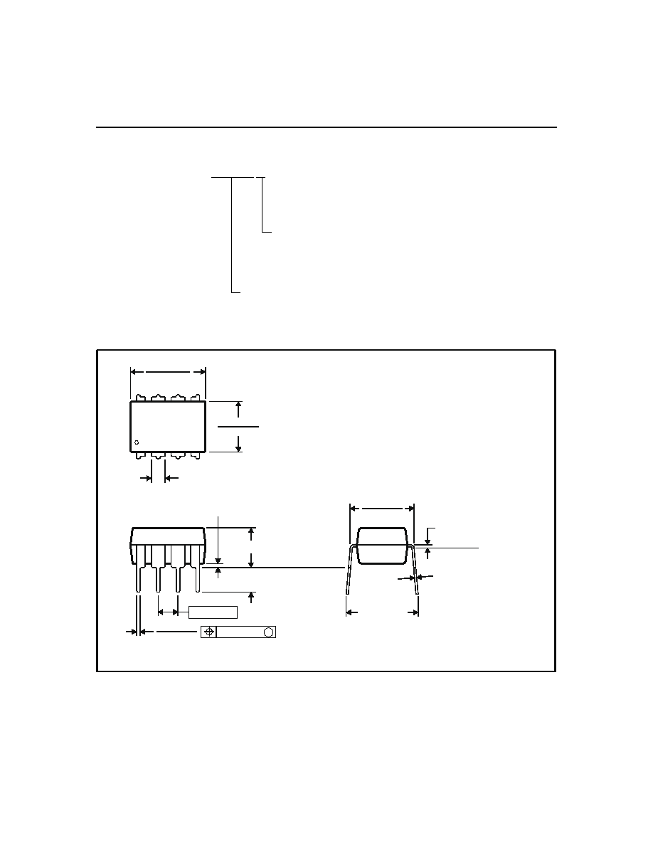
0.015 (0,38)
Gage Plane
0.325 (8,26)
0.300 (7,62)
0.010 (0,25) NOM
MAX
0.430 (10,92)
4040082/D 05/98
0.200 (5,08) MAX
0.125 (3,18) MIN
5
0.355 (9,02)
0.020 (0,51) MIN
0.070 (1,78) MAX
0.240 (6,10)
0.260 (6,60)
0.400 (10,60)
1
0.015 (0,38)
0.021 (0,53)
Seating Plane
M
0 .01 0 (0 ,2 5)
0.100 (2,54)
8-Pin DIP (P)
NOTES:
A. All linear dimensions are in inches (millimeters).
B. This drawing is subject to change without notice.
C. Falls within JEDEC MS-001
13
bq24400
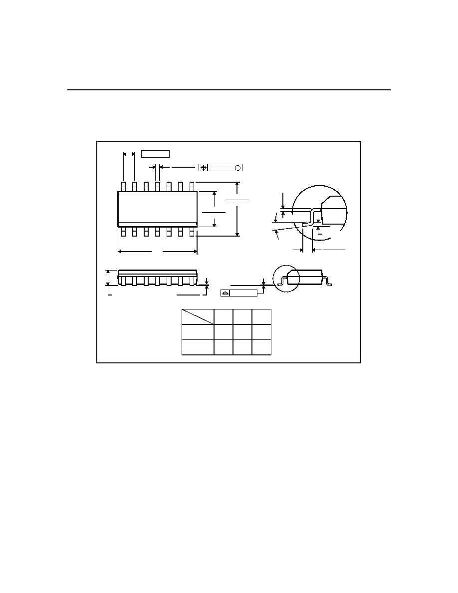
14 PINS SHOWN
4 0 4 0 0 4 7 / D 1 0 /9 6
0.228 (5,80)
0.244 (6,20)
0.069 (1,75) MAX
0.010 (0,25)
0.004 (0,10)
1
14
0.014 (0,35)
0.020 (0,51)
A
0.157 (4,00)
0.150 (3,81)
7
8
0.044 (1,12)
0.016 (0,40)
Seating Plane
0.010 (0,25)
PINS **
0.008 (0,20) NOM
A MIN
A MAX
DIM
Gage Plane
0.189
(4,80)
(5,00)
0.197
8
(8,55)
(8,75)
0.337
14
0.344
(9,80)
16
0.394
(10,00)
0.386
0.004 (0,10)
M
0 .0 1 0 (0 ,2 5 )
0.050 (1,27)
05- 85
8-Pin SOIC Narrow (D)
NOTES:
A. All linear dimensions are in inches (millimeters).
B. This drawing is subject to change without notice.
C. Body dimensions do not include mold flash or protrusion, not to exceed 0.006 (0,15).
D. Falls within JEDEC MS-012
14
bq24400
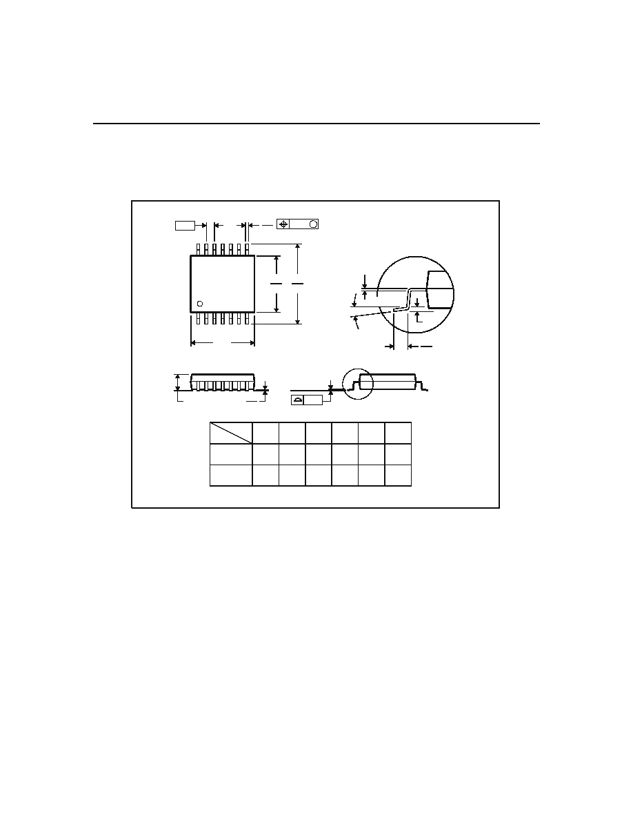
14 PINS SHOWN
0,65
M
0 ,1 0
0,10
0,25
0,50
0,75
0,15 NOM
Gage Plane
28
9,80
9,60
24
7,90
7,70
20
16
6,60
6,40
4040064/F 01/97
0,30
6,60
6,20
8
0,19
4,30
4,50
7
0,15
14
A
1
1,20 MAX
14
5,10
4,90
8
3,10
2,90
A MAX
A MIN
DIM
PINS **
0,05
4,90
5,10
Seating Plane
05- 85
NOTES:
A. All linear dimensions are in millimeters.
B. This drawing is subject to change without notice.
C. Body dimensions do not include mold flash or protrusion not to exceed 0,15.
D. Falls within JEDEC MO-153
8-Pin TSSOP ~ PW Package Suffix

15
IMPORTANT NOTICE
Texas Instruments and its subsidiaries (TI) reserve the right to make changes to their products or to discontinue any
product or service without notice, and advise customers to obtain the latest version of relevant information to verify,
before placing orders, that information being relied on is current and complete. All products are sold subject to the
terms and conditions of sale supplied at the time of order acknowledgement, including those pertaining to warranty,
patent infringement, and limitation of liability.
TI warrants performance of its semiconductor products to the specifications applicable at the time of sale in accor-
dance with TI's standard warranty. Testing and other quality control techniques are utilized to the extent TI deems
necessary to support this warranty. Specific testing of all parameters of each device is not necessarily performed, ex-
cept those mandated by government requirements.
CERTAIN APPLICATIONS USING SEMICONDUCTOR PRODUCTS MAY INVOLVE POTENTIAL RISKS OF DEATH,
PERSONAL INJURY, OR SEVERE PROPERTY OR ENVIRONMENTAL DAMAGE ("CRITICAL APPLICATIONS"). TI
SEMICONDUCTOR PRODUCTS ARE NOT DESIGNED, AUTHORIZED, OR WARRANTED TO BE SUITABLE FOR
USE IN LIFE-SUPPORT DEVICES OR SYSTEMS OR OTHER CRITICAL APPLICATIONS. INCLUSION OF TI
PRODUCTS IN SUCH APPLICATIONS IS UNDERSTOOD TO BE FULLY AT THE CUSTOMER'S RISK.
In order to minimize risks associated with the customer's applications, adequate design and operating safeguards
must be provided by the customer to minimize inherent or procedural hazards.
TI assumes no liability for applications assistance or customer product design. TI does not warrant or represent that
any license, either express or implied, is granted under any patent right, copyright, mask work right, or other intellec-
tual property right of TI covering or relating to any combination, machine, or process in which such semiconductor
products or services might be or are used. TI's publication of information regarding any third party's products or ser-
vices does not constitute TI's approval, warranty or endorsement thereof.
Copyright © 1999, Texas Instruments Incorporated