bq24702, bq24703
SLUS553D - MAY 2003 - REVISED JULY 2005
MULTICHEMISTRY BATTERY CHARGER CONTROLLER
AND SYSTEM POWER SELECTOR
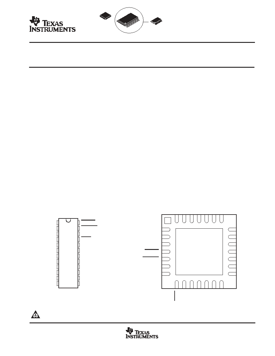
(6,60 mm x 7,90 mm)
Actual Size
1
www.ti.com
FEATURES
D
Dynamic Power Management, DPM
Minimizes Battery Charge Time
D
Integrated Selector Supports Battery
Conditioning and Smart Battery Learn Cycle
D
Zero Volt Operation
D
Selector Feedback Circuit Ensures
Break-Before-Make Transition
D
±
0.4% Charge Voltage Accuracy, Suitable for
Charging Li-Ion Cells
D
±
4% Charge Current Accuracy
D
300-kHz Integrated PWM Controller for
High-Efficiency Buck Regulation
D
Depleted Battery Detection and Indication to
Protect Battery From Over Discharge
D
20-
µ
A Sleep Mode Current for Low Battery
Drain
D
24-Pin TSSOP Package and 5 mm
◊
5 mm
QFN package (bq24703 only)
DESCRIPTION
The bq24702/bq24703 is a highly integrated battery
charge controller and selector tailored for notebook and
sub-notebook PC applications.
The bq24702/bq24703 uses dynamic power
management (DPM) to minimize battery charge time by
maximizing use of available wall-adapter power. This is
achieved by dynamically adjusting the battery charge
current based on the total system (adapter) current.
The bq24702/bq24703 uses a fixed frequency, pulse
width modulator (PWM) to accurately control battery
charge current and voltage. Charge current limits can
be programmed from a keyboard controller DAC or by
external resistor dividers from the precision 5-V,
±
0.6%,
externally bypassed voltage reference (VREF),
supplied by the bq24702/bq24703.
1
2
3
4
5
6
7
8
9
10
11
12
24
23
22
21
20
19
18
17
16
15
14
13
ACDET
ACPRES
ACSEL
BATDEP
SRSET
ACSET
VREF
ENABLE
BATSET
COMP
ACN
ACP
ACDRV
BATDRV
VCC
PWM
VHSP
ALARM
VS
GND
SRP
SRN
IBAT
BATP
bq24702, bq24703
PW PACKAGE
(TOP VIEW)
8
9
10
11
12
13
14
ACSEL
ACPRES
ACDET
ACDRV
BATDRV
NC
VCC
ACN
ACP
NC
NC
BATP
IBAT
NC
28
27
26
25
24
23
22
1
2
3
4
5
6
7
BA
TDEP
SRSET
ACSET
VREF
ENABLE
BA
TSET
COMP
PWM
VHSP
ALARM
VS
GND
SRP
SRN
21
20
19
18
17
16
15
bq24703
RHD PACKAGE
(BOTTOM VIEW)
NC - No internal connection
Copyright
2003 - 2004, Texas Instruments Incorporated
Please be aware that an important notice concerning availability, standard warranty, and use in critical applications of Texas Instruments
semiconductor products and disclaimers thereto appears at the end of this data sheet.
PRODUCTION DATA information is current as of publication date.
Products conform to specifications per the terms of Texas Instruments
standard warranty. Production processing does not necessarily include
testing of all parameters.
bq24702, bq24703
SLUS553D - MAY 2003 - REVISED JULY 2005
2
www.ti.com
DESCRIPTION (continued)
The battery voltage limit can be programmed by using the internal 1.196-V,
±
0.5% precision reference, making it
suitable for the critical charging demands of lithium-ion cells. Also, the bq24702/bq24703 provides an option to
override the precision reference and drive the error amplifier either directly from an external reference or from a
resistor divider off the 5 V supplied by the integrated circuit.
The selector function allows the manual selection of the system power source, battery or wall-adapter power. The
bq24702/bq24703 supports battery-conditioning and battery-learn cycles through the ACSEL function. The ACSEL
function allows manual selection of the battery or wall power as the main system power. It also provides autonomous
switching to the remaining source (battery or ac power) should the selected system power source terminate (refer
to Table 1 for the differences between the bq24702 and the bq24703). The bq24702/bq24703 also provides an alarm
function to indicate a depleted battery condition.
The bq24702/bq24703 PWM controller is ideally suited for operation in a buck converter for applications when the
wall-adapter voltage is greater than the battery voltage.
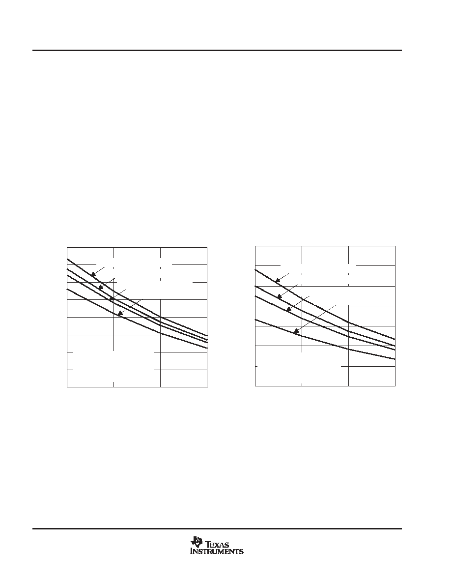
DISSIPATION RATINGS
0
0.20
0.40
0.60
0.80
1
1.20
1.40
1.60
25
50
70
85
MAX Pd (W) @ 500 LFM
MAX Pd (W) @ 250 LFM
MAX Pd (W) @ 150 LFM
MAX Pd (W) @ 0 LFM
JA = 89.37 C/W @ 0 LFM,
JA = 77.98 C/W @ 150 LFM,
JA = 73.93 C/W @ 250 LFM,
JA = 68.23 C/W @ 500 LFM
Maximum Power Dissipation (High K Board) - W
MAXIMUM POWER DISSIPATION
(HIGH K BOARD)
vs
FREE-AIR TEMPERATURE
TA - Free-Air Temperature -
∞
C
0
0.20
0.40
0.60
0.80
1
1.20
1.40
25
50
70
85
MAX Pd (W) @ 500 LFM
MAX Pd (W) @ 250 LFM
MAX Pd (W) @ 150 LFM
MAX Pd (W) @ 0 LFM
JA = 150.17 C/W @ 0 LFM,
JA = 110.95 C/W @ 150 LFM,
JA = 99.81 C/W @ 250 LFM,
JA = 86.03 C/W @ 500 LFM
Maximum Power Dissipation (Low K Board) - W
MAXIMUM POWER DISSIPATION
(LOW K BOARD)
vs
FREE-AIR TEMPERATURE
TA - Free-Air Temperature -
∞
C
The JEDEC low K (1s) board design used to derive this data was a 3-inch x 3-inch, two layer board with 2 ounce copper traces on top of the board.
The JEDEC high K (1s) board design used to derive this data was a 3-inch x 3-inch, multilayer board with 1 ounce internal power and ground
planes and 2 ounce copper traces on top and bottom of the board.

bq24702, bq24703
SLUS553D - MAY 2003 - REVISED JULY 2005
3
www.ti.com
Table 1. Available Options
CONDITION
SELECTOR OPERATION
CONDITION
-20
∞
C
TJ
125
∞
C
bq24702PW
bq24703RHD
Battery as Power Source
Battery removal
Automatically selects ac + alarm
Automatically selects ac + alarm
Battery reinserted
Selection based on selector inputs
Adapter latched until adapter is removed or ac select
toggles.
AC as Power Source
AC removal
Automatically selects battery
Automatically selects battery
AC reinserted
Selection based on selector inputs
Selection based on selector inputs
Depleted Battery Condition
Battery as power source
Sends ALARM signal
Automatically selects ac
Sends ALARM signal
AC as power source
Sends ALARM signal
Sends ALARM signal
ALARM Signal Active
Depleted battery condition
Depleted battery condition
When selector input is not equal to selector
output (single pulse alarm)
ABSOLUTE MAXIMUM RATINGS OVER OPERATING FREE-AIR TEMPERATURE
(unless otherwise noted)
}
Supply voltage range: VCC
-0.3 V to 30 V
. . . . . . . . . . . . . . . . . . . . . . . . . . . . . . . . . . . . . . . . . . . . . . . . . . . . . . . . .
Battery voltage range: SRP, SRN
-0.3 V to 30 V
. . . . . . . . . . . . . . . . . . . . . . . . . . . . . . . . . . . . . . . . . . . . . . . . . . . .
Input voltage: ACN, ACP
-0.3 V to 30 V
. . . . . . . . . . . . . . . . . . . . . . . . . . . . . . . . . . . . . . . . . . . . . . . . . . . . . . . . . . .
Virtual junction temperature range, T
J
-40
∞
C to 125
∞
C
. . . . . . . . . . . . . . . . . . . . . . . . . . . . . . . . . . . . . . . . . . . . . . .
Maximum source/sink current VHSP
50
mA
. . . . . . . . . . . . . . . . . . . . . . . . . . . . . . . . . . . . . . . . . . . . . . . . . . . . . . . .
Maximum ramp rate for V
CC
10 V/
µ
s
. . . . . . . . . . . . . . . . . . . . . . . . . . . . . . . . . . . . . . . . . . . . . . . . . . . . . . . . . . . . . .
Maximum sink current ACPRES, COMP, ALARM
2.5 mA
. . . . . . . . . . . . . . . . . . . . . . . . . . . . . . . . . . . . . . . . . . . . .
Maximum ramp rate for V
(BAT)
10 V/
µ
s
. . . . . . . . . . . . . . . . . . . . . . . . . . . . . . . . . . . . . . . . . . . . . . . . . . . . . . . . . . . .
Maximum source/sink current BATDRV
10 mA
. . . . . . . . . . . . . . . . . . . . . . . . . . . . . . . . . . . . . . . . . . . . . . . . . . . . . .
Maximum source/sink current ACDRV
10 mA
. . . . . . . . . . . . . . . . . . . . . . . . . . . . . . . . . . . . . . . . . . . . . . . . . . . . . . .
Maximum source/sink current PWM
50 mA
. . . . . . . . . . . . . . . . . . . . . . . . . . . . . . . . . . . . . . . . . . . . . . . . . . . . . . . . .
Maximum source/sink current pulsed ACDRV, (
10-
µ
s rise time, 10-
µ
s fall time, 1-ms pulse width, single pulse
) 50 mA
Maximum source current VREF
30 mA
. . . . . . . . . . . . . . . . . . . . . . . . . . . . . . . . . . . . . . . . . . . . . . . . . . . . . . . . . . . .
Maximum source current SRP
100 mA
. . . . . . . . . . . . . . . . . . . . . . . . . . . . . . . . . . . . . . . . . . . . . . . . . . . . . . . . . . . .
Maximum difference voltage SRP - SRN
30 V
. . . . . . . . . . . . . . . . . . . . . . . . . . . . . . . . . . . . . . . . . . . . . . . . . . . . . .
Storage temperature range T
stg
-65
∞
C to 150
∞
C
. . . . . . . . . . . . . . . . . . . . . . . . . . . . . . . . . . . . . . . . . . . . . . . . . . . .
Lead temperature (soldering, 10 seconds)
300
∞
C
. . . . . . . . . . . . . . . . . . . . . . . . . . . . . . . . . . . . . . . . . . . . . . . . . . .
Stresses beyond those listed under "absolute maximum ratings" may cause permanent damage to the device. These are stress ratings only, and
functional operation of the device at these or any other conditions beyond those indicated under "recommended operating conditions" is not
implied. Exposure to absolute-maximum-rated conditions for extended periods may affect device reliability.
All voltages are with respect to ground. Currents are positive into and negative out of the specified terminals. Consult the Packaging section of
the data book for thermal limitations and considerations of the package.

bq24702, bq24703
SLUS553D - MAY 2003 - REVISED JULY 2005
4
www.ti.com
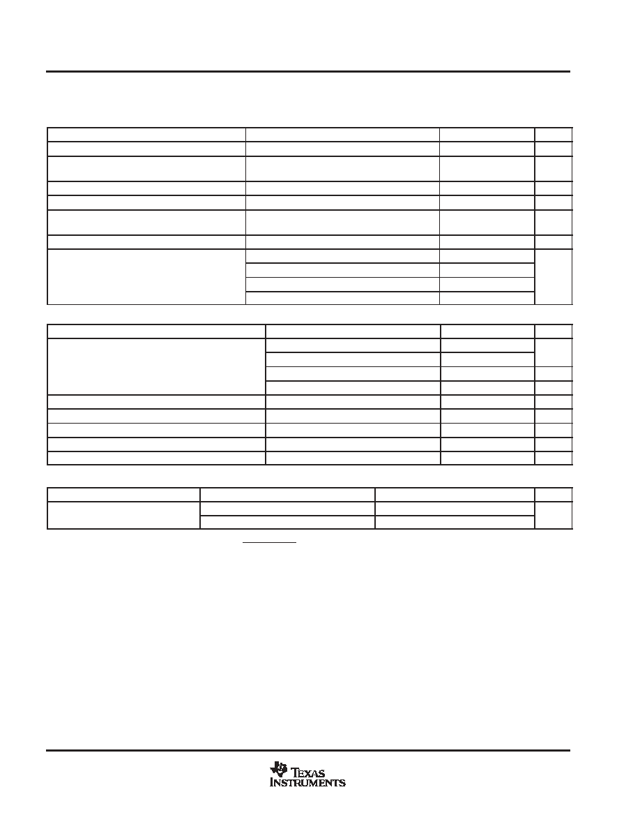
RECOMMENDED OPERATING CONDITIONS
(TA = TOPR) all voltages relative to Vss
MIN
MAX
UNIT
Supply voltage, (VCC)
Analog and PWM operation
7.0
28
V
Supply voltage, (VCC)
Selector operation
4.5
28
V
Negative ac current sense, (ACN)
7.0
28
V
Positive ac current sense, (ACP)
7.0
28
V
Negative battery current sense, (SRN)
5
28
V
Positive battery current sense, (SRP)
5
28
V
AC or adapter power detection (ACDET)
0
5
V
AC power indicator (ACPRES)
0
5
V
AC adapter power select (ACSEL)
0
5
V
Depleted battery level (BATDEP)
0
5
V
Battery charge current programming voltage (SRSET)
0
2.5
V
Charge enable (ENABLE)
0
5
V
External override to an internal 0.5% precision reference (BATSET)
0
2.5
V
Inverting input to the PWM comparator (COMP)
0
5
V
Battery charge regulation voltage measurement input to the battery--voltage gm amplifier (BATP)
0
5
V
Battery current differential amplifier output (IBAT)
0
5
V
System load voltage input pin (VS)
0
2.5
V
Depleted battery alarm output (ALARM)
0
5
V
Gate drive output (PWM)
VHSP
VCC
V
Battery power source select output (BATDRV)
0
28
V
AC or adapter power source selection output (ACDRV)
VHSP
VCC
V
ACSET
0
2.5
V
Operating free-air temperature, TA
-40
85
∞
C

bq24702, bq24703
SLUS553D - MAY 2003 - REVISED JULY 2005
5
www.ti.com
ELECTRICAL CHARACTERISTICS
(-40
∞
C
TJ
125
∞
C, 7.0 VDC
VCC
28 VDC, all voltages relative to Vss) (unless otherwise specified)
Quiescent Current
PARAMETER
TEST CONDITIONS
MIN
TYP
MAX
UNIT
IDD(OP)
Total chip operating current
ACPRES = High, EN = 0
1
1.6
6
mA
IDD(SLEEP) Total battery sleep current, ac not present
ACPRES = Low
22
28
µ
A
logic interface dc characteristics
PARAMETER
TEST CONDITIONS
MIN
TYP
MAX
UNIT
VOL
Low-level output voltage (ACPRES, ALARM)
IOL = 1 mA
0.4
V
VIL
Low-level input voltage (ACSEL, ENABLE)
0.6
V
VIH
High-level input voltage (ACSEL, ENABLE)
1.8
V
I(SINK1)
Sink current (ACPRES)
VOL = 0.4
1.5
2
2.5
mA
I(SINK2)
Sink current (ALARM)
VOL = 0.4
1.5
2
2.5
mA
PWM Oscillator
PARAMETER
TEST CONDITIONS
MIN
TYP
MAX
UNIT
fOSC(PWM) Oscillator frequency
0
∞
C
TJ
85
∞
C
260
300
340
kHz
fOSC(PWM) Oscillator frequency
-40
∞
C
TJ
125
∞
C
240
300
350
kHz
Maximum duty cycle
100%
Input voltage for maximum dc (COMP)
3.8
V
Minimum duty cycle
0%
Input voltage for minimum dc (COMP)
0.8
V(RAMP)
Oscillator ramp voltage (peak-to-peak)
1.85
2.15
2.30
V
VIK(COMP)
Internal input clamp voltage
(tracks COMP voltage for maximum dc)
3.8
4.5
V
IS(COMP)
Internal source current (COMP)
Error amplifier = OFF, V(COMP) = 1 V
70
110
140
µ
A
Leakage Current
PARAMETER
TEST CONDITIONS
MIN
TYP
MAX
UNIT
IL(ACDET)
Leakage current, ACDET
V(ACDET) = 5 V
0.2
µ
A
IL(SRSET)
Leakage current, SRSET
V(SRSET) = 2.5 V
0.2
µ
A
IL(ACSET)
Leakage current, ACSET
V(ACSET) = 2.5 V
0.2
µ
A
IL(BATDEP)
Leakage current, BATDEP
V(BATDEP) = 5 V
0.2
µ
A
IL(VS)
Leakage current, VS
V(VS) = 5 V
0.2
µ
A
IL(ALARM)
Leakage current, ALARM
V(ALARM) = 5 V
0.2
µ
A
IL(ACSEL)
Leakage current, ACSEL
V(ACSEL) = 5 V
0.2
µ
A
IL(ENABLE)
Leakage current, ENABLE
V(ENABLE) = 5 V
0.2
µ
A
IL(ACPRES)
Leakage current, ACPRES
V(ACPRES) = 5 V
0.2
µ
A
IL(BATP)
Leakage current, BATP
V(BATP) = 5 V
0.2
µ
A
IL(BATSET)
Leakage current, BATSET
V(BATSET) = 2.5 V
0.2
µ
A

bq24702, bq24703
SLUS553D - MAY 2003 - REVISED JULY 2005
6
www.ti.com
ELECTRICAL CHARACTERISTICS
(CONTINUED)
(-40
∞
C
TJ
125
∞
C, 7.0 VDC
VCC
28 VDC, all voltages relative to Vss) (unless otherwise specified)
Battery Current-Sense Amplifier
PARAMETER
TEST CONDITIONS
MIN
TYP
MAX
UNIT
gm
Transconductance gain
75
120
175
mA/V
CMRR
Common-mode rejection ratio
See Note 1
90
dB
VICR
Common-mode input (SRP, SRN)
voltage range
VCC = SRN, SRP + 2 V
5
30
V
I(SINK)
Sink current (COMP)
COMP = 1 V,
(SRP - SRN) = 10 mV
0.5
1.5
2.5
mA
IIB
Input bias current (SRP), See Note 2
V(SRP) = 16 V,
(SRP - SRN) = 100 mV
SRSET = 2.5 V,
VCC = 28
70
85
110
A
IIB
Input bias current accuracy
(ISRP - ISRN)
(SRP - SRN) = 100 mV, SRSET= 2.5 V,
VCC = 28 V, 0
TJ
125
∞
C
-3
0
3
µ
A
V(SET)
Battery current programming voltage
(SRSET)
0
2.5
V
AV
Battery current set gain
0.65 V
SRSET
2.5 V, 8 V
SRN
16 V,
See Note 3
24
25
26
V/V
Total battery current-sense mid-scale
SRSET = 1.25 V, TJ = 25
∞
C, See Note 4
-5%
5%
Total battery current-sense mid-scale
accuracy
SRSET = 1.25 V, See Note 4
-6%
6%
Total battery current-sense full-scale
SRSET = 2.5 V, TJ = 25
∞
C, See Note 4
-3%
3%
Total battery current-sense full-scale
accuracy
SRSET = 2.5 V, See Note 4
-4%
4%
NOTES: 1. Specified by design. Not production tested.
2
I(SRP) = I(SRN) = (V(SRSET) / 50 k
) + ((V(SRP) - V(SRN) / 3 k
)
example: If (V(SRSET) = 2.5 V) , (V(SRP) - V(SRN) = 100 mV) Then I(SRP) = I(SRN) = 83
µ
A
3. I
BAT
+
SRSET
R
SENSE
1
A
V
4. Total battery-current set is based on the measured value of (SRP-SRN) =
m, and the calculated value of (SRP-SRN) =
C, using
the measured gain, AV.
D
c
+
SRSET
A
V
, Total accuracy in %
+
(
D
m
* D
c)
D
c
100, I
(SRP)
*
I
(SRN)
+
0
bq24702, bq24703
SLUS553D - MAY 2003 - REVISED JULY 2005
7
www.ti.com
ELECTRICAL CHARACTERISTICS
(CONTINUED)
(-40
∞
C
TJ
125
∞
C, 7.0 VDC
VCC
28 VDC, all voltages relative to Vss) (unless otherwise specified)
Adapter Current-Sense Amplifier
PARAMETER
TEST CONDITIONS
MIN
TYP
MAX
UNIT
gm
Transconductance gain
75
130
175
mA/V
CMRR
Common-mode rejection ratio
See Note 1
90
dB
VICR
Common-mode input voltage range (ACP)
7.0
VCC
V
I(SINK)
Sink current (COMP)
COMP = 1 V, (ACP - ACN) = 10 mV
0.5
1.5
2.5
mA
IIB
Input bias current (ACP, ACN)
ACP = ACN = 28 V,
VCC = 28 V, ACSET = 2.5 V
40
50
65
A
IIB
Input bias current accuracy ratio
(I(ACP), I(ACN))
ACP = ACN = 28 V, VCC = 28 V,
ACSET = 2.5 V, 0
TJ
125
∞
C
-3
0
3
µ
A
V(SET)
AC current programming voltage (ACSET)
0
2.5
V
AV
AC current set gain
0.65 V
ACSET
2.5 V, 12 V
ACP
20 V,
See Note 5
24.5
25.3
26.5
V/V
Total ac current-sense mid-scale accuracy
ACSET = 1.25 V, TJ = 25
∞
C, See Note 6
-5%
5%
Total ac current-sense mid-scale accuracy
ACSET = 1.25 V, See Note 6
-6%
6%
Total ac current-sense full-scale accuracy
ACSET = 2.5 V, TJ = 25
∞
C, See Note 6
-3.5%
3.5%
Total ac current-sense full-scale accuracy
ACSET = 2.5 V, See Note 6
-4%
4%
Battery Voltage Error Amplifier
PARAMETER
TEST CONDITIONS
MIN
TYP
MAX
UNIT
gm
Transconductance gain
75
135
175
mA/V
CMRR
Common-mode rejection ratio
See Note 1
90
dB
VICR
BATSET common-mode input voltage range
1
2.5
V
VIT
Internal reference override input threshold voltage
0.20
0.25
0.35
V
I(SINK)
Sink current COMP
COMP = 1 V,
(BATP - BATSET) = 10 mV,
BATSET = 1.25 V
0.5
1.5
2.5
mA
TJ = 25
∞
C
1.190
1.196
1.202
V(FB)
Error-amplifier precision reference voltage
TJ = 0
∞
C to 85
∞
C
1.183
1.196
1.203
V
V(FB)
Error-amplifier precision reference voltage
TJ = -40
∞
C to 125
∞
C
1.178
1.196
1.204
V
NOTE:
5. Calculation of the ac current: I
AC
+
ACSET
R
SENSE
1
A
V
6. Total ac-current set accuracy is based on the measured value of (ACP-ACN) =
c, using the measured gain, AV.
D
c
+
ACSET
A
V
, Total accuracy in %
+
(
D
m
* D
c)
D
c
100, I
(ACP)
*
I
(ACN)
+
0
bq24702, bq24703
SLUS553D - MAY 2003 - REVISED JULY 2005
8
www.ti.com
ELECTRICAL CHARACTERISTICS
(CONTINUED)
(-40
∞
C
TJ
125
∞
C, 7.0 VDC
VCC
28 VDC, all voltages relative to Vss) (unless otherwise specified)
Battery Current Output Amplifier
PARAMETER
TEST CONDITIONS
MIN
TYP
MAX
UNIT
G(TR)
Transfer gain
(SRP - SRN) = 5 mV, See Note 7
20
V/V
VI(BAT)
Battery current readback output
voltage (IBAT)
(SRP - SRN) = 5 mV, SRP = 12 V,
VCC = 18 V, TJ = 25
∞
C
100
mV
Line rejection voltage
TJ = 25
∞
C
10
mV/V
CM
Common-mode input range (SRP)
5
28
V
VO(IBAT)
Battery current output voltage range
(IBAT)
0
2.5
V
IS(O)
Output source current (IBAT)
(SRP - SRN) = 100 mV
5
7.1
9.4
mA
(SRP - SRN) = 50 mV, TJ = 25
∞
C, See Note 7
-3%
2.4%
Total battery current readback
(SRP - SRN) = 50 mV, 0
∞
C
TJ
85
∞
C
-20%
20%
Total battery current readback
full-scale accuracy
(SRP - SRN) = 100 mV, TJ = 25
∞
C, See Note 7
-1.5%
1.2%
full-scale accuracy
(SRP - SRN) = 100 mV, 0
∞
C < TJ < 85
∞
C
-6%
8.5%
5-V Voltage Reference
PARAMETER
TEST CONDITIONS
MIN
TYP
MAX
UNIT
TJ = 25
∞
C
4.985
5
5.013
V
Vref
Output voltage (VREF)
TJ = 0
∞
C to 85
∞
C
4.946
5
5.013
V
Vref
Output voltage (VREF)
TJ = 40
∞
C to 85
∞
C
4.946
5
5.03
V
TJ = -40
∞
C to 125
∞
C
4.926
5
5.03
V
Line regulation
ILOAD = 5 mA
0.1
0.37
mV/V
Load regulation
1 mA
ILOAD
5 mA
1.1
4
mV/mA
Short circuit current
8
20
30
mA
5V REF output capacitor
Capacitance
2.2
10
µ
F
Output capacitor equivalent resistor
ESR
5
1000
m
Half Supply Regulator
PARAMETER
TEST CONDITIONS
MIN
TYP
MAX
UNIT
V(HSP)
Voltage regulation
I(SINK) = 20 mA, VCC = 18 V
VCC - 11
VCC - 10.2
VCC - 8.5
V
V(HSP)
Voltage regulation
I(SINK) = 1 mA, VCC = 7 V
1.5
V
NOTE:
7. Battery readback transfer gain G
TR
+
V
IBAT
(SRP
*
SRN)

bq24702, bq24703
SLUS553D - MAY 2003 - REVISED JULY 2005
9
www.ti.com
ELECTRICAL CHARACTERISTICS
(CONTINUED)
(-40
∞
C
TJ
125
∞
C, 7.0 VDC
VCC
28 VDC, all voltages relative to Vss) (unless otherwise specified)
MOSFET Gate Drive
PARAMETER
TEST CONDITIONS
MIN
TYP
MAX
UNIT
AC driver RDS(on) high
VCC = 18 V, I(ACDRV) = 1 mA
85
150
AC driver RDS(on) low
VCC = 18 V, I(ACDRV) = 1 mA
55
110
Battery driver RDS(on) high
VCC = 18 V, I(BATDRV) = 1 mA
315
600
Battery driver RDS(on) low
VCC = 18 V, I(BATDRV) = 1 mA
70
115
tda
Time delay from ac driver off to battery
driver on
ACSEL 2.4 V
0.2 V
1.2
2
µ
s
tdb
Time delay from battery driver off to ac
driver on
ACSEL 0.2 V
2.4 V
2.4
3.3
µ
s
VOH
PWM driver high-level output voltage
IO = -10 mA, VCC = 18 V
VCC -0.18 VCC -0.09
V
VOH
PWM driver high-level output voltage
IO = -50 mA, VCC = 18 V
VCC -1.2
VCC -0.8
V
PWM driver RDS(on) high
7
14
VOL
PWM driver low-level output voltage
IO = 10 mA, VCC = 18 V
VHSP+0.1
VHSP+0.4
V
VOL
PWM driver low-level output voltage
IO = 50 mA, VCC = 18 V
VHSP+0.6
VHSP+1.2
V
PWM driver RDS(on) low
5
8.5
Selector
PARAMETER
TEST CONDITIONS
MIN
TYP
MAX
UNIT
V(ACPRES)
AC presence detect voltage
1.194
1.246
1.286
V
V(ACPRES)
AC presence detect voltage
-40
∞
C to 85
∞
C
1.208
1.246
1.285
V
VIT(ACPRES) AC presence hysteresis
1%
td(ACPRES)
Deglitch delay for adapter insertion
100
µ
s
V(BATDEP)
Battery depletion ALARM trip voltage
See Note 8
1.194
1.246
1.286
V
V(BATDEP)
Battery depletion ALARM trip voltage
-40
∞
C to 85
∞
C
1.208
1.246
1.285
V
V(NOBAT)
No battery detect, switch to ACDRV
bq24702 only, See Note 8
0.869
1
1.144
V
V(NOBAT)
No battery detect, switch to ACDRV
-40
∞
C to 85
∞
C
0.880
1
1.118
V
t(BATSEL)
Battery select time (ACSEL low to BATDRV low)
VS < BATP, 50% threshold,
ACSEL 2.4 V
0.2 V
1
2.5
3.5
µ
s
t(ACSEL)
AC select time (ACSEL high to ACDRV low)
ACSEL 0.2 V
2.4 V
1
2.5
3.5
µ
s
V(VS)
VS voltage to enable BATDRV
BATP = 1 V
0.98
1
1.02
V
VIT(VS)
VS voltage hysteresis
VS > BATP
20
35
85
mV
Zero Volt Operation
PARAMETER
TEST CONDITIONS
MIN
TYP
MAX
UNIT
rDS(on)
Static drain source on-state resistance
VCC = 7 V, TJ = 125
∞
C, IO = 100 mA
5.3
8.7
zero volt operation threshold
BATDEP increasing
0.743
0.794
0.840
V
zero volt operation threshold
BATDEP decreasing
0.570
0.62
0.656
V
NOTES: 8. Total battery current readback accuracy is based on the measured value of VIBAT, VIBATm, and the calculated value of VIBAT,
VIBATc, using the measured value of the transfer gain, GTR.
V
IBATc
+
(SRP
*
SRN)
GTR
Total Accuracy in %
+
V
IBATm
*
V
IBATc
V
IBATm
100
9. Refer to Table 1 to determine the logic operation of the bq24702 and the bq24703.
bq24702, bq24703
SLUS553D - MAY 2003 - REVISED JULY 2005
10
www.ti.com
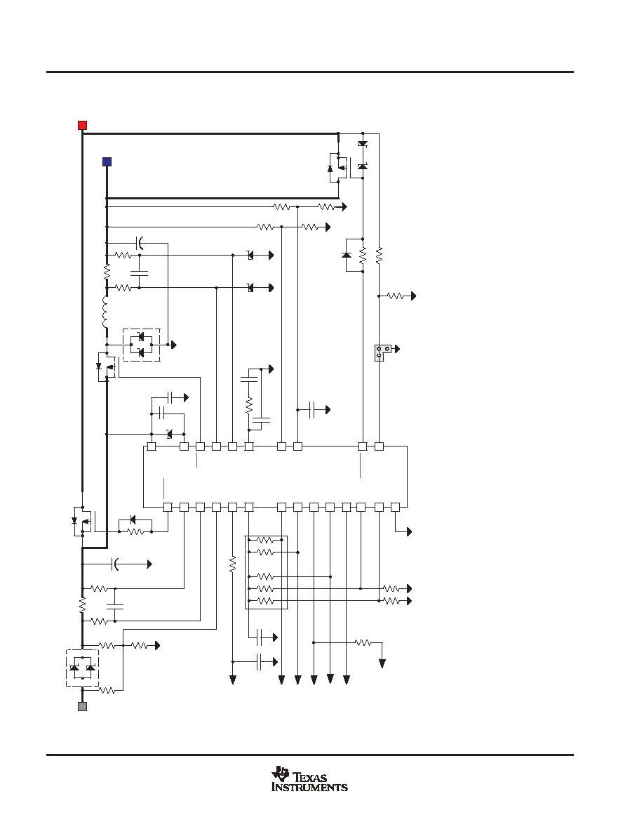
APPLICATION DIAGRAM
R6
R1
1
Open
R12
Note
1
R14
0.025
R13
R15
C3
C12
35
V
U2
SI4435DY
R18
D2
BAS16
ACDRV
24
ACN
11
12
ACP
1
ACDET
22
VCC
20
VHSP
D3
13 V
21
SRP
C6
16V
C7
35 V
PWM
L1
U3
SI4435DY
R20
SRN
D5
Note 1
D6
Note 1
R22
R23
Note
1
R24
R25
Note
1
16
15
BA
TDEP
BA
TP
4
13
R16
C5
C4
150pF
10
COMP
D1
MBRD640CTT4
D4
MBRD640CTT4
C1
1
35 V
R21
Note
1
R19
Note
1
C8
U4
SI4435DY
D9
BAS16
R26
100K
BA
TDRV
23
SYSTEM
R27
R28
Note
1
Battery Plus
VS
18
AC
Adapter
VREF
7
ENABLE
ACSEL
3
8
19
ALARM
ACPRES
2
C1
ENABLE
ACSEL
ALARM
ACPRES
5
6
SRSET
ACSET
R2
R10
Note
1
R8
Note
1
C10
180pF
14
IBA
T
C13
1 nF
IBA
T
R29
17
GND
9
BA
TSET
BA
TSET
100 k
100
1
µ
F
100
10
33
µ
H
4.7
µ
F
1
µ
F
0.025
22
µ
F
100
4.7
µ
F
604 k
Connect to GND
to Disable
100 k
30 k
4.7
µ
F
Note 1:
R8 Sets
AC
Adapter Current Limit
R10 Sets Charge Current
R12
Sets
AC
ADAPTER Current Limit
R23 Sets the Battery Depleted
Threshold
R25 Sets the Charge Regulation V
oltage
R28 Sets System Break Before Make
R19 = R21, Sets Zero V
olt Charge Current
bq24703
bq24702
Note
1
604 k
604 k
Note
1
Note
1
C1
1 Optional, See
Application
Notes
C12 For V
alue, See
Application
Notes
C8 V
alue Depends on R21 and R19, See
Application
Notes
D5, D6 Refer to the
Application
Section
PROCESSOR'S
POWER SUPPL
Y
bq24702, bq24703
SLUS553D - MAY 2003 - REVISED JULY 2005
11
www.ti.com
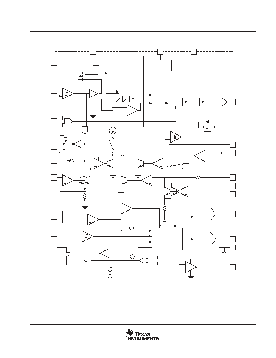
BLOCK DIAGRAM
UDG-00137
20
VHSP
VHSP
REGULATOR
22
VCC
7
VREF
VOLTAGE
REFERENCE
VREF
ACPRES
2
ACPRES
+
1
ACDET
ACPRES
HYST
LEVEL
SHIFT
S
Q
Q
R
PWM
LOGIC
OSC
21
HIGH-SIDE
DRIVE
300 kHz
+
3
ACSEL
8
ENABLE
VCC
VHSP
10
COMP
5 V
100
µ
A
+
+
5 V
SRN
+
2 k
12
ACP
11
ACN
+
6
ACSET
25
k
VCC
ac
CURRENT
ERROR
AMPLIFIER
BATTERY
CURRENT
ERROR
AMPLIFIER
BATTERY
VOLTAGE
ERROR
AMPLIFIER
+
13
PWM
BATP
9
BATSET
16
SRP
2 k
15
SRN
5
SRSET
25
k
0.25 V
BATTERY
SELECT
DRIVE
ADAPTER
SELECT
DRIVE
+
24
VCC
VHSP
VCC
23
BATDRV
BATTERY SELECT
LOGIC
AND
ANTI-CROSS
CONDUCT
+
NO BATTERY
COMPARATOR
17
GND
+
A=20
VCC
14
IBAT
SRP
SRN
ACSEL
ACPRES
+
SWITCH TO
BATTERY
4
BATDEP
+
DEPLETED
BATTERY
COMPARATOR
BATP
18
VS
2
2
1
1
ACDRV
ACDRV
ACSEL
bq24702 ONLY
bq24703 ONLY
19
ALARM
2 V
+
BATDA
VTBD
Zero Volt
Charging
VACPRES
VFB
0.8 x VNOBAT
VBATDEP

bq24702, bq24703
SLUS553D - MAY 2003 - REVISED JULY 2005
12
www.ti.com
Terminal Functions
TERMINAL
NAME
bq24702
(PW)
bq24703
(QFN)
I/O
DESCRIPTION
ACDET
1
26
I
AC or adapter power detection
ACDRV
24
25
O
AC or adapter power source selection output
ACN
11
8
I
Negative differential input
ACP
12
9
I
Positive differential input
ACPRES
2
27
O
AC power indicator
ACSEL
3
28
I
AC adapter power select
ACSET
6
3
I
Adapter current programming voltage
ALARM
19
19
O
Alarm output
BATDEP
4
1
I
Depleted battery level
BATDRV
23
24
O
Battery power source select output
BATP
13
12
I
Battery charge regulation voltage measurement input to the battery-voltage gm amplifier
BATSET
9
6
I
External override to an internal precision reference
COMP
10
7
O
Inverting input to the PWM comparator
ENABLE
8
5
I
Charge enable
GND
17
17
O
Supply return and ground reference
IBAT
14
13
O
Battery current differential amplifier output
PWM
21
21
O
Gate drive output
SRN
15
15
I
Negative differential battery current sense amplifier input
SRP
16
16
I/O
Positive differential battery current sense amplifier input
SRSET
5
2
I
Battery charge current programming voltage
VCC
22
22
I
Operational supply voltage
VHSP
20
20
O
Voltage source to drive gates of the external MOSFETs
VREF
7
4
O
Precision 5-V reference
VS
18
18
I
System (load) voltage input pin

bq24702, bq24703
SLUS553D - MAY 2003 - REVISED JULY 2005
13
www.ti.com
Pin Assignments
ACDET: AC or adapter power detection. This input pin is used to determine the presence of the ac adapter.
When the voltage level on the ACDET pin is less than V
ACPRES
, the bq24702/bq24703 is in sleep mode, the
PWM control is disabled, the BATDRV is driven low, and the ACDRV is driven high. This feature can be used
to automatically select battery as the system power source.
ACDRV: AC or adapter power source select output. This pin drives an external P-channel MOSFET used to
switch to the ac wall-adapter as the system power source. When the ACSEL pin is high while the voltage on
the ACDET pin is greater than V
ACPRES
, the output ACDRV pin is driven low (V
HSP
). This pin is driven high (V
CC
)
when the ACDET is less than V
ACPRES
.
ACN, ACP: Negative and positive differential inputs, respectively for ac-to-dc adapter current sense resistor.
ACPRES: This open-drain output pin is used to indicate the presence of ac power. A logic high indicates there
is a valid ac input. A low indicates the loss of ac power. ACPRES is high when the voltage level on the ACDET
pin is greater than V
ACPRES
.
ACSEL: AC adapter power select. This input selects either the ac adapter or the battery as the power source.
A logic high selects ac power, while a logic low selects the battery.
ACSET: Adapter current programming voltage. This input sets the system current level at which dynamic power
management occurs. Adapter currents above this programmed level activate the dynamic power management
and proportionally reduce the available power to the battery.
ALARM: Depleted battery alarm output. This open-drain pin indicates that a depleted battery condition exists.
A pullup on ALARM goes high when the voltage on the BATDEP pin is below V
ACPRES
. On the bq24702, the
ALARM output also activates when the selector inputs do not match the selector state.
BATDEP: Depleted battery level. A voltage divider network from the battery to BATDEP pin is used to set the
battery voltage level at which depletion is indicated by the ALARM pin. See ALARM pin for more details. A
battery depletion is detected when BATDEP is less than V
ACPRES
. A no-battery condition is detected when the
battery voltage is < 80% of the depleted threshold. In a no-battery condition, the bq24702 automatically selects
ac as the input source. If ENABLE = 1, the PWM remains enabled.
BATDRV: Battery power source select output. This pin drives an external P-channel MOSFET used to switch
the battery as the system's power source. When the voltage level on the ACDET pin is less than V
ACPRES
, the
output of the BATDRV pin is driven low, GND. This pin is driven high (V
CC
) when ACSEL is high and ACDET
> V
ACPRES
.
BATP: Battery charge regulation voltage measurement input to the battery-voltage g
m
amplifier. The voltage
on this pin is typically derived from a voltage divider network connected across the battery. In a voltage loop,
BATP is regulated to the V
FB
precision reference of the battery voltage g
m
amplifier.
BATSET: An external override to an internal precision reference. When BATSET is > 0.25 V, the voltage level
on the BATSET pin sets the voltage charge level. When BATSET
0.25 V, an internal V
FB
reference is
connected to the inverting input of the battery error amplifier. To ensure proper battery voltage regulation with
BATSET, BATSET must be > 1.0 V. Simply ground BATSET to use the internal reference.
COMP: The inverting input to the PWM comparator and output of the g
m
amplifiers. A type II compensation
network between COMP and GND is recommended.
ENABLE: Charge enable. A high on this input pin allows PWM control operation to enable charging while a low
on this pin disables and forces the PWM output to a high state. Battery charging is initiated by asserting a logic
1 on the ENABLE pin.
GND: Supply return and ground reference
IBAT: Battery current differential amplifier output. The output of this pin produces a voltage proportional to the
battery charge current. This voltage is suitable for driving an ADC input.

bq24702, bq24703
SLUS553D - MAY 2003 - REVISED JULY 2005
14
www.ti.com
PWM: Gate drive output pin drives the P-channel MOSFET for PWM control. The PWM control is active when
ACPRES, ACSEL, and ENABLE are high. PWM is driven low to V
HSP
and high to V
CC
.
SRN, SRP: Differential amplifier inputs for battery current sense. These pins feed back the battery charge
current for PWM control. SRN is tied to the battery terminal. SRP is the source pin for zero volt operation.
SRSET: Battery charge current programmed voltage. The level on this pin sets the battery charge current limit.
VCC: Operational supply voltage.
VHSP: The VHSP pin is connected to a 1-
µ
F capacitor (close to the pin) to provide a stable voltage source to
drive the gates of the external MOSFETs. VHSP = VCC - 10 V for VCC > 10.5 V and VHSP = VCC - 0.5 V for
VCC <10.5 V. A 13-V Zener diode should be placed between VCC and VHSP to prevent MOSFET overstress
during start-up.
VREF: Bypassed precision voltage 5-V output. It can be used to set fixed levels on the inverting inputs of any
one of the three error amplifiers if desired. The tight tolerance is suitable for charging lithium-ion batteries.
VS: System (Load) voltage input pin. The voltage on this pin indicates the system voltage in order to insure a
break before make transition when changing from ac power to battery power. The battery is protected from an
over-voltage condition by disabling the P-channel MOSFET connected to the BATDRV pin if the voltage at VS
is greater than BATP. This function can be eliminated by grounding the VS pin.

bq24702, bq24703
SLUS553D - MAY 2003 - REVISED JULY 2005
15
www.ti.com
APPLICATION INFORMATION
Programming the Thresholds
The input-referenced thresholds for battery depleted, ac detection and charge voltage are defined by
dimensioning the external dividers connected to pins BATDEP, ACDET and BATP. This calculation is simple,
and consists of assuming that when the input voltage equals the desired threshold value the voltage at the
related pin is equal to the pin internal reference voltage:
Vinput = Vpin
◊
(1 + Kres)
where:
Vinput = Target threshold, referenced to input signal
Vpin = Internal reference(1.196 V for BATP; 1.246 V for BATDEP, ACDET)
Kres = External resistive divider gain ( for instance: R24/R25 for BATP)
When using external dividers with high absolute value the input bias currents for those pins must be included
in the threshold calculation. On the bq24702/3 the input bias currents increase the actual value for the threshold
voltage, when compared to the values calculated using the internal references and divider gain only:
Vinput = Vpin
◊
(1+Kres) + Vbias
The increase on the threshold voltage is given by:
Vbias = Rdiv
◊
Ipin
where:
Vbias = Voltage increase due to pin bias current
Rdiv = External resistor value for resistor connected from pin to input voltage
Ipin = Maximum pin leakage current
The effect of IB can be reduced if the resistor values are decreased.
Dynamic Power Management
The dynamic power management (DPM) feature allows a cost effective choice of an ac wall-adapter that
accommodates 90% of the system's operating-current requirements. It minimizes battery charge time by
allocating available power to charge the battery (i.e. I
BAT
= I
ADPT
- I
SYS
). If the system plus battery charge
current exceeds the adapter current limit, as shown in Figure 1, the DPM feature reduces the battery charge
current to maintain an overall input current consumption within user defined power capability of the wall-adapter.
As the system's current requirements decrease, additional current can be directed to the battery, thereby
increasing battery charge current and minimizing battery charge time.
The DPM feature is inherently designed into the PWM controller by inclusion of the three control loops,
battery-charge regulation voltage, battery-charge current, and adapter-charge current, refer to Figure 2. If any
of the three user programmed limits are reached, the corresponding control loop commands the PWM controller
to reduce duty cycle, thereby reducing the battery charge current.
bq24702, bq24703
SLUS553D - MAY 2003 - REVISED JULY 2005
16
www.ti.com
UDG-00113
NO
CHARGE
MAXIMUM
CHARGE CURRENT
DYNAMIC POWER
MANAGEMENT
MAXIMUM
CHARGE CURRENT
ADAPTER CURRENT
SYSTEM CURRENT
BATTERY CHARGE CURRENT
ADAPTER CURRENT LIMIT
Figure 1. Dynamic Power Management
ACDET Operation
The ACDET function senses the loss of adequate adapter power. If the voltage on ACDET drops below the
internal V
ACPRES
reference voltage, a loss of ADAPTER power is declared and the bq24702/bq24703 switches
to battery power as the main system power. In addition, the bq24702/bq24703 shuts down its 5-V VREF and
enters a low power sleep mode.
Battery Charger Operation
The bq24702/bq24703 fixed-frequency, PWM controller is designed to provide closed-loop control of battery
charge-current (I
CH
) based on three parameters, battery-float voltage (V
BAT
), battery-charge current, and
adapter charge current (I
ADPT
). The bq24702/bq24703 is designed primarily for control of a buck converter
using a high side P-channel MOSFET device (SW, refer to Figure 2).
The three control parameters are voltage programmable through resistor dividers from the bq24702/bq24703
precision 5-V reference, an external or internal precision reference, or directly via a DAC interface from a
keyboard controller.
Adapter and battery-charge current information is sensed and fed back to two transconductance (g
m
) amplifiers
via low-value-sense resistors in series with the adapter and battery respectively. Battery voltage information is
sensed through an external resistor divider and fed back from the battery to a third g
m
amplifier.
Precharge Operation
The precharge operation must be performed using the PWM regulator. The host can set the precharge current
externally by monitoring the ALARM pin to detect a battery depleted condition and programming SRSET voltage
to obtain the desired precharge current level.
bq24702, bq24703
SLUS553D - MAY 2003 - REVISED JULY 2005
17
www.ti.com
Zero Volt Operating
The zero volt operation is intended to provide a low current path to close open packs and protect the system
in the event of a pack cell short-circuit condition or if a short is applied to the pack terminal. It is not designed
to precharge depleted packs, as it is disabled at voltages that are not within normal pack operating range for
precharge.
If the voltage at BATDEP pin is below the zero volt operation threshold , charge is enabled (EN=HI), and ac is
selected (ACSEL=HI) the bq24702/3 enters the zero volt operation mode. When the zero volt operation mode
is on, the internal PWM is disabled, and an internal power MOSFET connects SRP to V
CC
. The battery charge
current is limited by the filter resistor connected to SRP pin (R19). R19 must be dimensioned to withstand the
worst case power dissipation when in zero volt operation mode.
The zero volt operation mode is disabled when BATDEP is above the zero volt operation threshold, and the main
PWM loop is turned on if charge is enabled, regulating the current to the value set by SRSET voltage. To avoid
errors on the charge current both resistors on the SRP, SRN filter must have the same value. Note, however,
that R21 (connected to SRN) does not dissipate any power when in zero volt operation and can be of minimum
size.
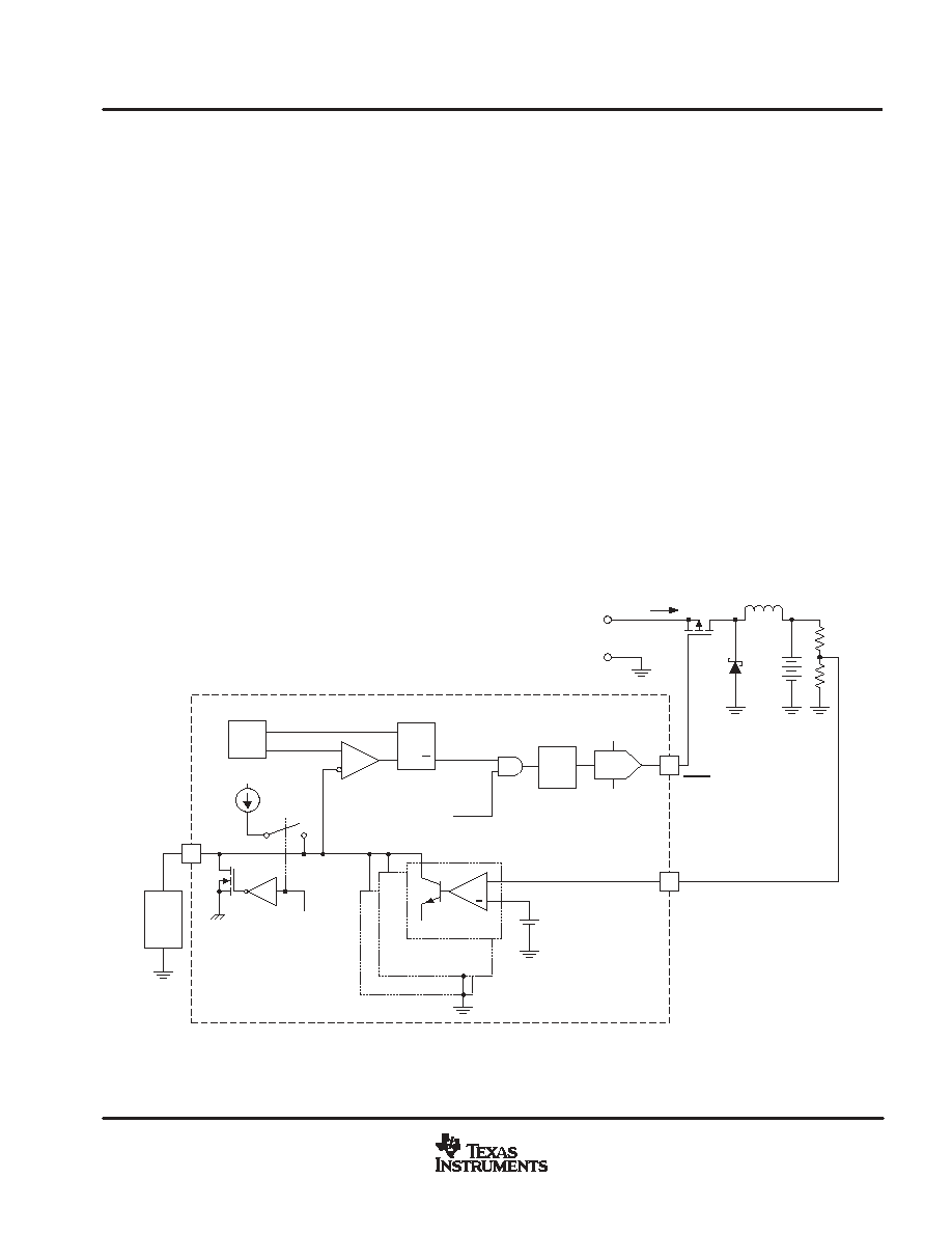
PWM Operation
The three open collector g
m
amplifiers are tied to the COMP pin (refer to Figure 2), which is internally biased
up by a 100-
µ
A constant current source. The voltage on the COMP pin is the control voltage (V
C
) for the PWM
comparator. The PWM comparator compares V
C
to the sawtooth ramp of the internally fixed 300-kHz oscillator
to provide duty cycle information for the PWM drive. The PWM drive is level-shifted to provide adequate gate
voltage levels for the external P-channel MOSFET. Refer to PWM selector switch gate drive section for gate
drive voltage levels.
UDG-00114
10
21
100
µ
A
ENABLE
5 V
OSC
CLK
RAMP
S
Q
Q
R
ENABLE
LATCH OUT
FROM ENABLE LOGIC
PWM COMPARATOR
LEVEL
SHIFT
PWM
DRIVE
VHSP
VCC
+
1.25 V
BATTERY
VOLTAGE
BATTERY CHARGE
CURRENT
ADP CURRENT
Z
COMP
COMP
+
V
ADPT
+
I
SW
SW
V
BAT
gm
AMPLIFIERS
PWM
BATP
13
Q1
D1
Figure 2. PWM Controller Block Diagram

bq24702, bq24703
SLUS553D - MAY 2003 - REVISED JULY 2005
18
www.ti.com
Softstart
Softstart is provided to ensure an orderly start-up when the PWM is enabled. When the PWM controller is
disabled (ENABLE = Low), the 100-
µ
A current source pullup is disabled and the COMP pin is actively pulled
down to GND. Disabling the 100-
µ
A pullup reduces current drain when the PWM is disabled. When the
bq24702/bq24703 PWM is enabled (ENABLE = High), the COMP pin is released and the 100-
µ
A pullup is
enabled (refer to Figure 2). The voltage on the COMP pin increases as the pullup charges the external
compensation network connected to the COMP pin. As the voltage on the COMP pin increases the PWM duty
cycle increases linearly as shown in Figure 3.
Figure 3
10
0
30
20
40
60
50
70
90
80
100
VCOMP - Compensation Voltage - V
Percent Duty Cycle - %
PERCENT DUTY CYCLE
vs
COMPENSATION VOLTAGE
1.2
1.7
2.2
2.7
3.2
As any one of the three controlling loops approaches the programmed limit, the g
m
amplifier begins to shunt
current away from the COMP pin. The rate of voltage rise on the COMP pin slows due to the decrease in total
current out of the pin, decreasing the rate of duty cycle increase. When the loop has reached the programmed
limit the g
m
amplifier shunts the entire bias current (100
µ
A) and the duty cycle remains fixed. If any of the control
parameters tries to exceed the programmed limit, the g
m
amplifier shunts additional current from the COMP pin,
further reducing the PWM duty cycle until the offending parameter is brought into check.
Setting the Battery Charge Regulation Voltage
The battery charge regulation voltage is programmed through the BATSET pin, if the internal precision
reference is not used. The BATSET input is a high-impedance input that is driven by either a keyboard controller
DAC or via a resistor divider from a precision reference (see Figure 4).
The battery voltage is fed back to the g
m
amplifier through a resistor divider network. The battery charge
regulation voltage can be defined as:
V
BATTERY
+
(R1
)
R2)
V
BATSET
R2
V
)
I
BATP
R1
where I
BATP
= input bias current for pin BATP
(1)
bq24702, bq24703
SLUS553D - MAY 2003 - REVISED JULY 2005
19
www.ti.com
The overall accuracy of the battery charge regulation voltage is a function of the bypassed 5-V reference voltage
tolerance as well as the tolerances on R1 and R2. The precision voltage reference has a 0.5% tolerance making
it suitable for the tight battery voltage requirements of Li-ion batteries. Tolerance resistors of 0.1% are
recommended for R1 and R2 as well as any resistors used to set BATSET.
The bq24702/bq24703 provides the capability of using an internal precision voltage reference through the use
of a multiplexing scheme, refer to Figure 4, on the BATSET pin. When BATSET voltage is less than 0.25 V, an
internal reference is switched in and the BATSET pin is switched out from the g
m
amplifier input. When the
BATSET voltage is greater than 0.25 V, the BATSET pin voltage is switched in to the input of the g
m
amplifier
and the voltage reference is switched out.
NOTE:The minimum recommended BATSET is 1.0 V, if BATSET is used to set the voltage loop.
UDG-00116
(a) VBATSET < 0.25 V
(b) VBATSET > 1 V
13
+
9
0.25 V
BATSET
BATP
R2
VBAT
gm AMPLIFIER
1.196 V
R1
VREF = 5 V
COMP
13
9
+
10
0.25 V
BATSET
BATP
VBAT
gm AMPLIFIER
1.25 V
COMP
10
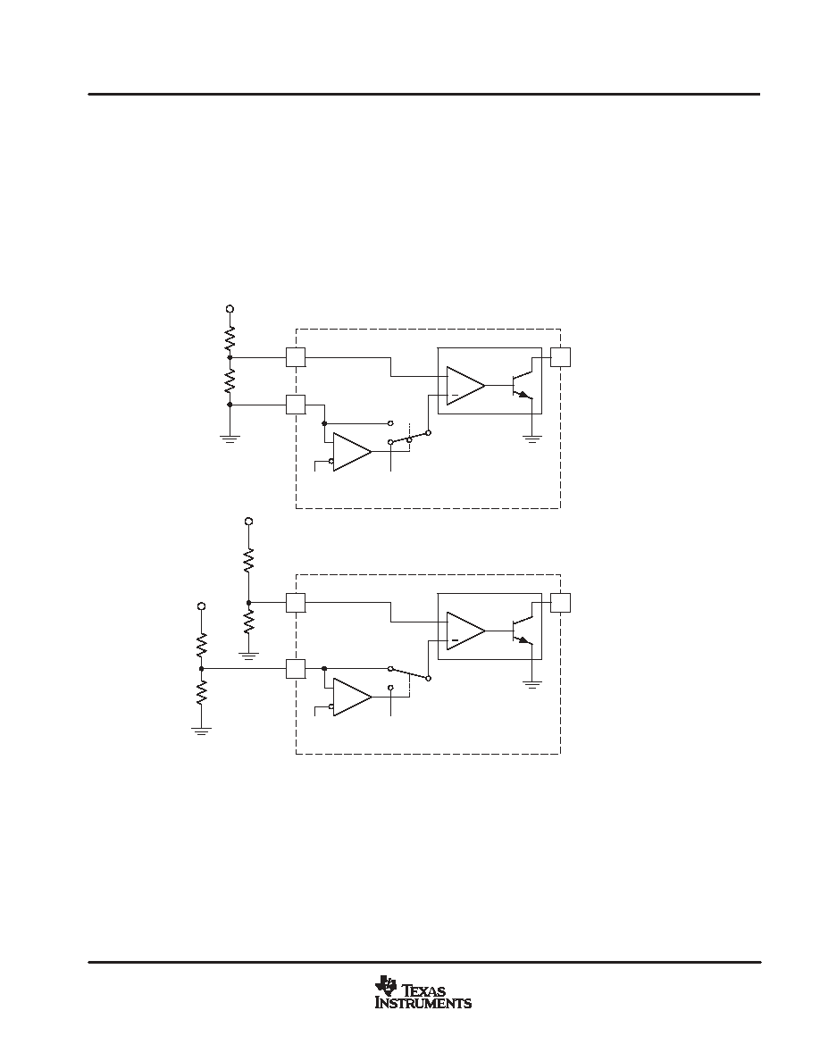
Figure 4. Battery Error Amplifier Input Multiplexing Scheme
bq24702, bq24703
SLUS553D - MAY 2003 - REVISED JULY 2005
20
www.ti.com
Programming the Battery Charge Current
The battery charge current is programmed via a voltage on the SRSET pin. This voltage can be derived from
a resistor divider from the 5-V VREF or by means of an DAC. The voltage is converted to a current source that
is used to develop a voltage drop across an internal offset resistor at one input of the SR g
m
amplifier. The charge
current is then a function of this voltage drop and the sense resistor (R
S
), refer to Figure 5.
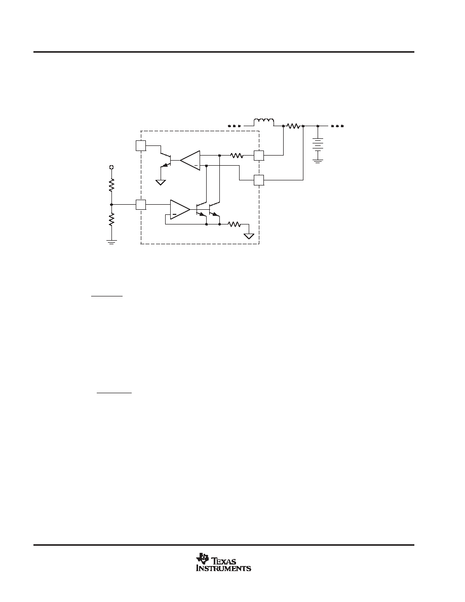
UDG-00117
RS
25 k
10
5
16
COMP
+
2 k
15
+
SRN
SRP
VREF
SRSET
Figure 5. Battery Charge Current Input Threshold Function
The battery charge current can be defined as:
I
BAT
+
V
SRSET
25
R
S
where V
SRSET
is the programming voltage on the SRSET pin. V
SRSET
maximum is 2.5 V.
Programming the Adapter Current
Like the battery charge current described previously, the adapter current is programmed via a voltage on the
ACSET pin. That voltage can either be from an external resistor divider from the 5-V VREF or from an external
DAC. The adapter current is defined as:
I
ADPT
+
V
ACSET
25
R
S2
(2)
(3)

bq24702, bq24703
SLUS553D - MAY 2003 - REVISED JULY 2005
21
www.ti.com
COMPONENT SELECTION
MOSFET Selection
MOSFET selection depends on several factors, namely, gate-source voltage, input voltage, and input current.
The MOSFET must be a P-channel device capable of handling at least 15-V gate-to-source with a drain-source
breakdown of V
BV
~ V
IN
+1 V. The average input current can be approximated by:
I
IN
(avg)
+
D
Ichg
A
D = Duty cycle
Ichg = Charge current
The RMS current through the MOSFET is defined as:
I
IN
(RMS)
+
Ichg
D
A
RMS
The rise/fall times for pin PWM for the selected MOSFET should be greater than 40 nsec.
Schottky Rectifier (Freewheeling)
The freewheeling Schottky rectifier must also be selected to withstand the input voltage, V
IN
. The average
current can be approximated from:
I
D1
(avg)
+
Ichg
(1
*
D) A
Choosing an Inductance
Low inductance values result in a steep current ramp or slope. Steeper current slopes result in the converter
operating in the discontinuous mode at a higher power level. Steeper current slopes also result in higher output
ripple current, which may require a higher number or more expensive capacitors to filter the higher ripple current.
In addition, the higher ripple current results in an error in the sensed battery current particularly at lower charging
currents. It is recommended that the ripple current not exceed 20% to 30% of full scale dc current.
L
+
D
V
IN
*
V
BAT
F
S
Ichg
Ripple
Ripple = % Ripple allowed (Ex.: 0,2 for 20% ripple)
Too large an inductor value results in the current waveform of Q1 and D1 in Figure 2 approximating a
squarewave with an almost flat current slope on the step. In this case, the inductor is usually much larger than
necessary, which may result in an efficiency loss (higher DCR) and an area penalty.
Selecting an Output Capacitor
For this application the output capacitor is used primarily to shunt the output ripple current away from the battery.
The output capacitor should be sized to handle the full output ripple current as defined as:
Ic (RMS)
+
V
IN
*
V
BAT
D
F
S
L
A
RMS
(4)
(5)
(6)
(7)
(8)

bq24702, bq24703
SLUS553D - MAY 2003 - REVISED JULY 2005
22
www.ti.com
Selecting an Input Capacitor
The input capacitor is used to shunt the converter ripple current on the input lines. The capacitor(s) must have
a ripple current (RMS) rating of:
I
RMS
+
[Ichg
(1≠D)]
2
D
)
[Ichg
D]
2
(1≠D)
A
RMS
In addition to shunting the converter input ripple when the PWM is operating, the input capacitor also acts as
part of an LC filter, where the inductance component is defined by the ac adapter cable inductance and board
trace inductance from adapter connector to filter capacitor. Overshoot conditions can be observed at V
CC
line
during fast load transients when the adapter powers the load or when the adapter is hot-plugged .
Increasing the input capacitor value decreases the overshoot at V
CC
. Avoid overshoot voltages at V
CC
in excess
of the absolute maximum ratings for that pin.
Compensating the Loop
For the bq24702/bq24703 used as a buck converter, the best method of compensation is to use a Type II
compensation network from the output of the transconductance amplifiers (COMP pin) to ground (GND) as
shown in Figure 2. A Type II compensation adds a pole-zero pair and an additional pole at dc.
The Type II compensation network places a zero at
F
Z
+
1
2
1
p
R
COMP
C
Z
Hz
and a pole at
F
P
+
1
2
1
p
R
COMP
C
P
Hz
For this battery charger application the following component values: C
Z
= 4.7
µ
F, C
P
= 150 pF, and
R
COMP
= 100
, provides a closed loop response with more than sufficient phase margin, as long as the LC
pole [1/2
◊
PI
◊
sqrt (l
◊
c)] is set below 10 kHz. The SRP/SRN filter (R19, R21, C8) and ACP/ACN filter
(R13/R15/C3) are required to filter noise associated with the PWM switching. To avoid adding secondary poles
to the PWM closed loop system those filters should be set with cutoff frequencies higher than 1 kHz.
Selector Operation
The bq24702/bq24703 allows the host controller to manually select the battery as the system's main power
source, without having to remove adapter power. This allows battery conditioning through smart battery learn
cycles. In addition, the bq24702/bq24703 supports autonomous supply selection during fault conditions on
either supply. The selector function uses low R
DS(on)
P-channel MOSFETs for reduced voltage drops and longer
battery run times.
NOTE: Selection of battery power whether manual or automatic results in the suspension of battery
charging.
(9)
(10)
(11)
bq24702, bq24703
SLUS553D - MAY 2003 - REVISED JULY 2005
23
www.ti.com
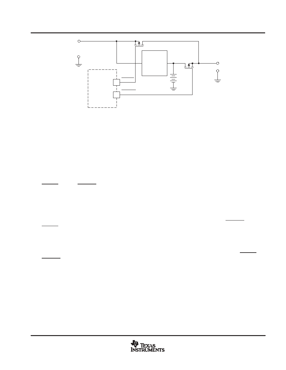
UDG-00119
(bq24702)
BATTERY
SELECTOR
CONTROL
BATDRV
24
23
ACDRV
BATTERY
SELECT
SWITCH
ADAPTER SELECT SWITCH
ADAPTER
INPUT
SYSTEM
LOAD
PWM
BATTERY
CHARGER
BAT
(bq24702)
Figure 6. Selector Control Switches
Autonomous Selection Operation
Adapter voltage information is sensed at the ACDET pin via a resistor divider from the adapter input. The voltage
on the ACDET pin is compared to an internally fixed threshold. An ACDET voltage less than the set threshold
is considered as a loss of adapter power regardless of the actual voltage at the adapter input. Information
concerning the status of adapter power is fed back to the host controller through ACPRES. The presence of
adapter power is indicated by ACPRES being set high. A loss of adapter power is indicated by ACPRES going
low regardless of which power source is powering the system. During a loss of adapter power, the
bq24702/bq24703 obtains operating power from the battery through the body diode of the P-channel battery
select MOSFET. Under a loss of adapter power, ACPRES (normally high) goes low, if adapter power is selected
to power the system, the bq24702/bq24703 automatically switches over to battery power by commanding
ACDRV high and BATDRV low. During the switch transition period, battery power is supplied to the load via the
body diode of the battery select P-channel MOSFET. When adapter power is restored, the bq24702/bq24703
configures the selector switches according to the state of signals; ACSEL, and ACPRES. If the ACSEL pin is
left high when ac power is restored, the bq24702/bq24703 automatically switches back to ac power. To remain
on battery power after ac power is restored, the ACSEL pin must be brought low.
Conversely, if the battery is removed while the system is running on battery power and adapter power is present,
the bq24702/bq24703 automatically switches over to adapter power by commanding BATDRV high and
ACDRV low.
NOTE: For the bq24702 any fault condition that results in the selector MOSFET switches not
matching their programmed states is indicated by the ALARM pin momentarily going high. Refer
to Battery Depletion Detection Section for more information on the ALARM discrete.
When switching between the ac adapter and battery the internal logic monitors the voltage at pins ACDRV and
BATDRV to implement a break-before-make function, with typical dead time on the order of 150 nsec.
The turnon times for the external ac/battery switches can be increased to minimize inrush peak currents; that
can be accomplished by adding external resistors in series with the MOSFET gates(R18 and R26). Note,
however, that adding those resistors effectively disables the internal break-before-make function for
ac/battery-switches, as the MOSFET gate voltages can not be monitored directly. If external resistors are added
to increase the rise/fall times for battery/ac switches the break-before-make has to be implemented with discrete
external components, to avoid shoot-through currents between ac adapter and battery pack. This functionality
can be implemented by adding diodes (D2/D9) that bypass the external resistors when turning off the external
FETs.

bq24702, bq24703
SLUS553D - MAY 2003 - REVISED JULY 2005
24
www.ti.com
Smart Learn Cycles When Adapter Power Is Present
Smart learn cycles can be conducted when adapter power is present by asserting and maintaining the ACSEL
pin low. The adapter power can be reselected at the end of the learn cycle by a setting ACSEL to a logic high,
provided that adapter power is present. Battery charging is suspended while selected as the system power
source.
NOTE: On the bq24703 the ac adapter is switched to the load when the battery voltage reaches
the battery depleted threshold; it can be used when the learn cycle does not require the battery
voltage to go below the battery depleted threshold. If the learn cycle algorithm requires the battery
voltage to go lower than the battery depleted voltage, the bq24702 should be used, as it does not
switch the ac adapter to load upon battery depleted detection.
System Break Before Make Function
When selecting the battery as the system primary power source, the adapter power select MOSFET turns off,
in a break-before-make fashion, before the battery select MOSFET turns on. To ensure that this happens under
all load conditions, the system voltage (load voltage) can be monitored through a resistor divider on the VS pin.
This function provides protection against switching over to battery power if the adapter selector switch were
shorted and adapter power present. Setting the VS resistive divider gain with the same gain selected for the
BATP resistive divider assures the battery switch is turned on only when the system voltage is equal or less than
the battery voltage. This function can be eliminated by grounding the VS pin.
The ACDET function senses the adapter voltage via a resistive divider (refer to application circuit).The divider
can be connected either to the anode of the input blocking diode (directly to the adapter supply) or to the cathode
of the input blocking diode (bq24702/3 VCC pin). When the divider is connected to the adapter supply, the
adapter power removal is immediately identified and the sleep mode is entered, disabling the
break-before-make function for system voltage (see section for system power switching) and coupling system
voltage to the battery line. In normal operation with a battery present, the battery low impedance prevents any
over-voltage conditions. However, if a pack is not present or the pack is open, the battery line voltage has a
transient equal to the adapter voltage. The bq24703 SRP/SRN pins are designed to withstand this over-voltage
condition, but avoid connection to the battery line of any external devices that are not rated to withstand the
adapter voltage.
Connecting the ACDET resistive divider input to the VCC node keeps the system break-before-make function
enabled until the voltage at pin VS is lower than the voltage at pin BATP. However, note that when using this
topology the VCC pin voltage can be held by capacitive loads at either the VCC or system (ac switch is on) nodes
when the ac adapter is removed. As the ACDET divider is connected to the VCC line there is a time delay from
ac adapter removal to ac adapter removal detection by the IC. This time is dependent on load conditions and
capacitive load values at VCC and system lines.
Battery Depletion Detection
The bq24702/bq24703 provides the host controller with a battery depletion discrete, the ALARM pin, to alert
the host when a depleted battery condition occurs. The battery depletion level is set by the voltage applied to
the BATDEP pin through a voltage divider network. The ALARM output asserts high and remains high as long
as the battery deplete condition exists, regardless of the power source selected.
For the bq24702, the host controller must take appropriate action during a battery deplete condition to select
the proper power source. The bq24702 remains on the selected power source. The bq24703, however,
automatically reverts over to adapter power, provided the adapter is present, during a deep discharge state. The
battery is considered as being in a deep discharge state when the battery voltage is less than (0.8
◊
depleted
level).
Feature sets for the bq24702 and bq24703 are detailed in Table 1.
bq24702, bq24703
SLUS553D - MAY 2003 - REVISED JULY 2005
25
www.ti.com
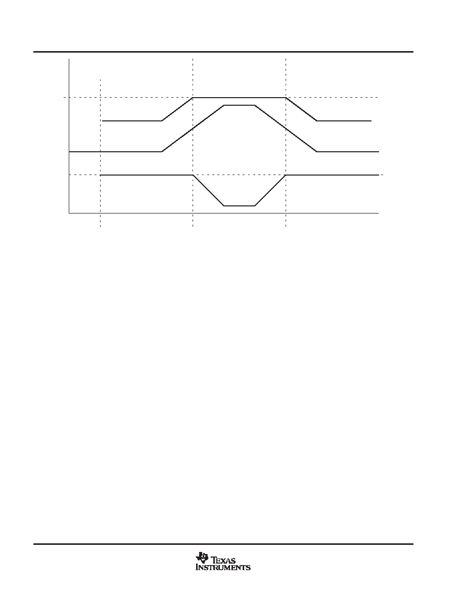
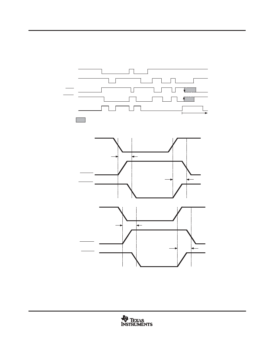
SELECTOR/ALARM TIMING EXAMPLE
The selector and ALARM timing example in Figure 7 illustrates the battery conditioning support.
NOTE: For manual selection of wall power as the main power source, both the ACPRES and
ACSEL signals must be a logic high.
UDG-00120
UDG-00122
ACPRES
ACSEL
BATDRV
ALARM
bq24703 ONLY
ACDRV
BATTERY
DEPLETE
CONDITION
BATDEP< 1 V
t
ACSEL
tBATSEL
ACSEL
(ACPRES)
tACSEL
tBATSEL
ACDRV
BATDRV
BATDRV
ACDRV
Figure 7. Battery Selector and ALARM Timing Diagram

bq24702, bq24703
SLUS553D - MAY 2003 - REVISED JULY 2005
26
www.ti.com
PWM SELECTOR SWITCH GATE DRIVE
Because the external P-channel MOSFETs (as well as the internal MOSFETs) have a maximum gate-source
voltage limitation of the input voltage, VCC, cannot be used directly to drive the MOSFET gate under all input
conditions. To provide safe MOSFET-gate-drive at input voltages of less than an intermediate gate drive voltage
rail was established (VSHP). Where V
HSP
= VCC - 10 V. This ensures adequate enhancement voltage across
all operating conditions.
An external zener diode (D3) connected between VCC and VHSP is required for transient protection; its
breakdown voltage should be above the maximum value for internal VHSP/VCC clamp voltage for all operating
conditions.
TRANSIENT CONDITIONS AT SYSTEM, OVER-VOLTAGE AT SYSTEM TERMINAL
Overshoot conditions can be observed at the system terminal due to fast load transients and inductive
characteristics of the system terminal to load connection. An overshoot at the system terminal can be directly
coupled to the VCC and VBAT nodes, depending on the switch mode of operation. If the capacitors at VBAT
and VCC can not reduce this overshoot to values below the absolute maximum ratings, it is recommended that
an additional capacitor is added to the system terminal to avoid damage to IC or external components due to
voltage overstress under those transient conditions.
AC ADAPTER COLLAPSING DUE TO TRANSIENT CONDITIONS
The ac adapter voltage collapses when the ac switch is on and a current load transient at the system exceeds
the adapter current limit protection. Under those conditions the ac switch is turned off when the ac adapter
voltage falls below the ac adapter detection threshold. If the system terminal to load impedance has an inductive
characteristic, a negative voltage spike can be generated at the system terminal and coupled into the battery
line via the battery switch backgate diode.
In normal operation, with a battery present, this is not an issue, as the low battery impedance holds the voltage
at battery line. However, if a battery is not present or the pack protector switches are open the negative spike
at the system terminal is directly coupled to the SRP/SRN pins via the R19/R21 resistors.
Avoid damage to the SRP/SRN pins if this transient condition happens in the application. If a negative voltage
spike happens at system terminal and R19/R21 limit the current sourced from the pin to less than -50 mA (Ipin
= Vsystem/R19), the pins SRP/SRN are not damaged and the external protection schottky diodes are not
required. However, if the current under those transient conditions exceeds -50 mA, external schottky diodes
must be added to clamp the voltage at pins SRP/SRN so they do not exceed the absolute maximum ratings
specified (-0.3 V).
IBAT AMPLIFIER
A filter with a cutoff frequency smaller than 10 kHz should be added to the IBAT output to remove switching
noise.
POWER DISSIPATION CALCULATION
During PWM operation, the power dissipated internally to the IC increases as the internal driver is switching the
PWM FET on/off. The power dissipation figures are dependent on the external FET used, and can be calculated
using the following equation:
Pd(max) = [IDDOP + Qg
◊
Fs(max)]
◊
VADAP
where:
Qg= Total gate charge for selected PWM MOSFET
IDDOP = Maximum quiescent current for IC
VADAP = Maximum adapter voltage
Fs(max) = Maximum PWM switching frequency
The maximum junction temperature for the IC must be limited to 125
∞
C, under worst case conditions.

bq24702, bq24703
SLUS553D - MAY 2003 - REVISED JULY 2005
27
www.ti.com
TYPICAL CHARACTERISTICS
Figure 8
1.175
1.18
1.185
1.19
1.195
1.2
1.205
1.21
1.215
-40
10
60
110
V
FB
Error
Amplifier Reference - V
-
VCC = 18 V
ERROR AMPLIFIER REFERENCE
vs
JUNCTION TEMPERATURE
TJ - Junction Temperature -
_
C
125
Figure 9
4.9
4.92
4.94
4.96
4.98
5
5.02
5.04
5.06
5.08
5.1
-40
10
60
110
VREF - 5 -V Reference - V
VCC = 18 V
BYPASSED 5-V REFERENCE
vs
JUNCTION TEMPERATURE
TJ - Junction Temperature -
_
C
125
Figure 10
TOTAL SLEEP CURRENT
vs
JUNCTION TEMPERATURE
TJ - Junction Temperature -
_
C
14
16
18
20
22
24
26
-40
10
60
110
I SLEEP
- Battery Sleep Current -
A
µ
VCC = 18 V
125
Figure 11
OSCILLATOR FREQUENCY
vs
JUNCTION TEMPERATURE
TJ - Junction Temperature -
_
C
235
245
255
265
275
285
295
305
315
325
335
-40
10
60
110
f - Oscillator Frequency - kHz
VCC = 18 V
125
bq24702, bq24703
SLUS553D - MAY 2003 - REVISED JULY 2005
28
www.ti.com
Figure 12
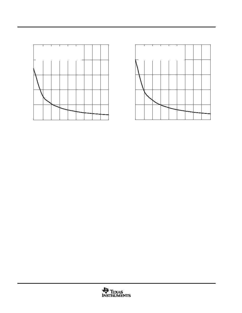
BATTERY CURRENT SET ACCURACY
vs
BATTERY CURRENT SET VOLTAGE
VSRSET - Battery Current Set Voltage - V
0
5
10
15
20
25
0.25
0.75
1.25
1.75
2.25
SRSET Full Scale = 2.5 V
= Max Programmed Current
TJ = 25
∞
C
Battery Current Set
Accuracy - %
0.5
1
1.5
2
2.5
Figure 13
AC CURRENT SET ACCURACY
vs
AC CURRENT SET VOLTAGE
VACSET - AC Current Set Voltage - V
0
5
10
15
20
25
0.25
0.75
1.25
1.75
2.25
AC Current Set
Accuracy - %
ACSET Full Scale = 2.5 V
= Max Programmed Current
TJ = 25
∞
C
0.5
1
1.5
2
2.5
BOARD LAYOUT GUIDELINES
Recommended Board Layout
Follow these guidelines when implementing the board layout:
1.
Do not place lines and components dedicated to battery/adapter voltage sensing (ACDET,BATDEP, VS),
voltage feedback loop (BATP, BATSET if external reference is used) and shunt voltage sensing
(SRP/SRN/ACP/ACN) close to lines that have signals with high dv/dt (PWM, BATDRV, ACDRV, VHSP) to
avoid noise coupling.
2.
Add filter capacitors for SRP/SRN (C8) and ACP/ACN (C3) close to IC pins
3.
Add Reference filter capacitor C1 close to IC pins
4.
Use an isolated, clean ground for IC ground pin and resistive dividers used in voltage sensing; use an
isolated power ground for PWM filter cap and diode (C11/D4). Connect the grounds to the battery PACK-
and adapter GND.
5.
Place C7 close to VCC pin.
6.
Place input capacitor C12 close to PWM switch (U3) source and R14.
7.
Position ac switch (U2) to minimize trace length from ac switch source to input capacitor C12.
8.
Minimize inductance of trace connecting PWM pin and PWM external switch U3 gate
9.
Maximize power dissipation planes connected to PWM switch
10. Maximize power dissipation planes connected to SRP resistor if steady state in zero volt mode is possible
11. Maximize power dissipation planes connected to D1

PACKAGING INFORMATION
Orderable Device
Status
(1)
Package
Type
Package
Drawing
Pins Package
Qty
Eco Plan
(2)
Lead/Ball Finish
MSL Peak Temp
(3)
BQ24702PW
ACTIVE
TSSOP
PW
24
60
Green (RoHS &
no Sb/Br)
CU NIPDAU
Level-1-260C-UNLIM
BQ24702PWG4
ACTIVE
TSSOP
PW
24
60
Green (RoHS &
no Sb/Br)
CU NIPDAU
Level-1-260C-UNLIM
BQ24702PWR
ACTIVE
TSSOP
PW
24
2000 Green (RoHS &
no Sb/Br)
CU NIPDAU
Level-1-260C-UNLIM
BQ24702PWRG4
ACTIVE
TSSOP
PW
24
2000 Green (RoHS &
no Sb/Br)
CU NIPDAU
Level-1-260C-UNLIM
BQ24703PW
ACTIVE
TSSOP
PW
24
60
Green (RoHS &
no Sb/Br)
CU NIPDAU
Level-1-260C-UNLIM
BQ24703PWR
ACTIVE
TSSOP
PW
24
2000 Green (RoHS &
no Sb/Br)
CU NIPDAU
Level-1-260C-UNLIM
BQ24703PWRG4
ACTIVE
TSSOP
PW
24
2000 Green (RoHS &
no Sb/Br)
CU NIPDAU
Level-1-260C-UNLIM
BQ24703RHDR
ACTIVE
QFN
RHD
28
3000 Green (RoHS &
no Sb/Br)
CU NIPDAU
Level-2-260C-1 YEAR
BQ24703RHDRG4
ACTIVE
QFN
RHD
28
3000 Green (RoHS &
no Sb/Br)
CU NIPDAU
Level-2-260C-1 YEAR
(1)
The marketing status values are defined as follows:
ACTIVE: Product device recommended for new designs.
LIFEBUY: TI has announced that the device will be discontinued, and a lifetime-buy period is in effect.
NRND: Not recommended for new designs. Device is in production to support existing customers, but TI does not recommend using this part in
a new design.
PREVIEW: Device has been announced but is not in production. Samples may or may not be available.
OBSOLETE: TI has discontinued the production of the device.
(2)
Eco
Plan
-
The
planned
eco-friendly
classification:
Pb-Free
(RoHS)
or
Green
(RoHS
&
no
Sb/Br)
-
please
check
http://www.ti.com/productcontent
for the latest availability information and additional product content details.
TBD: The Pb-Free/Green conversion plan has not been defined.
Pb-Free (RoHS): TI's terms "Lead-Free" or "Pb-Free" mean semiconductor products that are compatible with the current RoHS requirements
for all 6 substances, including the requirement that lead not exceed 0.1% by weight in homogeneous materials. Where designed to be soldered
at high temperatures, TI Pb-Free products are suitable for use in specified lead-free processes.
Green (RoHS & no Sb/Br): TI defines "Green" to mean Pb-Free (RoHS compatible), and free of Bromine (Br) and Antimony (Sb) based flame
retardants (Br or Sb do not exceed 0.1% by weight in homogeneous material)
(3)
MSL, Peak Temp. -- The Moisture Sensitivity Level rating according to the JEDEC industry standard classifications, and peak solder
temperature.
Important Information and Disclaimer:The information provided on this page represents TI's knowledge and belief as of the date that it is
provided. TI bases its knowledge and belief on information provided by third parties, and makes no representation or warranty as to the
accuracy of such information. Efforts are underway to better integrate information from third parties. TI has taken and continues to take
reasonable steps to provide representative and accurate information but may not have conducted destructive testing or chemical analysis on
incoming materials and chemicals. TI and TI suppliers consider certain information to be proprietary, and thus CAS numbers and other limited
information may not be available for release.
In no event shall TI's liability arising out of such information exceed the total purchase price of the TI part(s) at issue in this document sold by TI
to Customer on an annual basis.
PACKAGE OPTION ADDENDUM
www.ti.com
27-Sep-2005
Addendum-Page 1
MECHANICAL DATA
MTSS001C ≠ JANUARY 1995 ≠ REVISED FEBRUARY 1999
POST OFFICE BOX 655303
∑
DALLAS, TEXAS 75265
PW (R-PDSO-G**)
PLASTIC SMALL-OUTLINE PACKAGE
14 PINS SHOWN
0,65
M
0,10
0,10
0,25
0,50
0,75
0,15 NOM
Gage Plane
28
9,80
9,60
24
7,90
7,70
20
16
6,60
6,40
4040064/F 01/97
0,30
6,60
6,20
8
0,19
4,30
4,50
7
0,15
14
A
1
1,20 MAX
14
5,10
4,90
8
3,10
2,90
A MAX
A MIN
DIM
PINS **
0,05
4,90
5,10
Seating Plane
0
∞
≠ 8
∞
NOTES: A. All linear dimensions are in millimeters.
B. This drawing is subject to change without notice.
C. Body dimensions do not include mold flash or protrusion not to exceed 0,15.
D. Falls within JEDEC MO-153

IMPORTANT NOTICE
Texas Instruments Incorporated and its subsidiaries (TI) reserve the right to make corrections, modifications,
enhancements, improvements, and other changes to its products and services at any time and to discontinue
any product or service without notice. Customers should obtain the latest relevant information before placing
orders and should verify that such information is current and complete. All products are sold subject to TI's terms
and conditions of sale supplied at the time of order acknowledgment.
TI warrants performance of its hardware products to the specifications applicable at the time of sale in
accordance with TI's standard warranty. Testing and other quality control techniques are used to the extent TI
deems necessary to support this warranty. Except where mandated by government requirements, testing of all
parameters of each product is not necessarily performed.
TI assumes no liability for applications assistance or customer product design. Customers are responsible for
their products and applications using TI components. To minimize the risks associated with customer products
and applications, customers should provide adequate design and operating safeguards.
TI does not warrant or represent that any license, either express or implied, is granted under any TI patent right,
copyright, mask work right, or other TI intellectual property right relating to any combination, machine, or process
in which TI products or services are used. Information published by TI regarding third-party products or services
does not constitute a license from TI to use such products or services or a warranty or endorsement thereof.
Use of such information may require a license from a third party under the patents or other intellectual property
of the third party, or a license from TI under the patents or other intellectual property of TI.
Reproduction of information in TI data books or data sheets is permissible only if reproduction is without
alteration and is accompanied by all associated warranties, conditions, limitations, and notices. Reproduction
of this information with alteration is an unfair and deceptive business practice. TI is not responsible or liable for
such altered documentation.
Resale of TI products or services with statements different from or beyond the parameters stated by TI for that
product or service voids all express and any implied warranties for the associated TI product or service and
is an unfair and deceptive business practice. TI is not responsible or liable for any such statements.
Following are URLs where you can obtain information on other Texas Instruments products and application
solutions:
Products
Applications
Amplifiers
amplifier.ti.com
Audio
www.ti.com/audio
Data Converters
dataconverter.ti.com
Automotive
www.ti.com/automotive
DSP
dsp.ti.com
Broadband
www.ti.com/broadband
Interface
interface.ti.com
Digital Control
www.ti.com/digitalcontrol
Logic
logic.ti.com
Military
www.ti.com/military
Power Mgmt
power.ti.com
Optical Networking
www.ti.com/opticalnetwork
Microcontrollers
microcontroller.ti.com
Security
www.ti.com/security
Telephony
www.ti.com/telephony
Video & Imaging
www.ti.com/video
Wireless
www.ti.com/wireless
Mailing Address:
Texas Instruments
Post Office Box 655303 Dallas, Texas 75265
Copyright
2005, Texas Instruments Incorporated