Äîêóìåíòàöèÿ è îïèñàíèÿ www.docs.chipfind.ru
www.ti.com
FEATURES
APPLICATIONS
DESCRIPTION
32
31
30
29
28
27
25
13
14
15
16
17
18
19
20
33
34
35
36
37
38
39
40
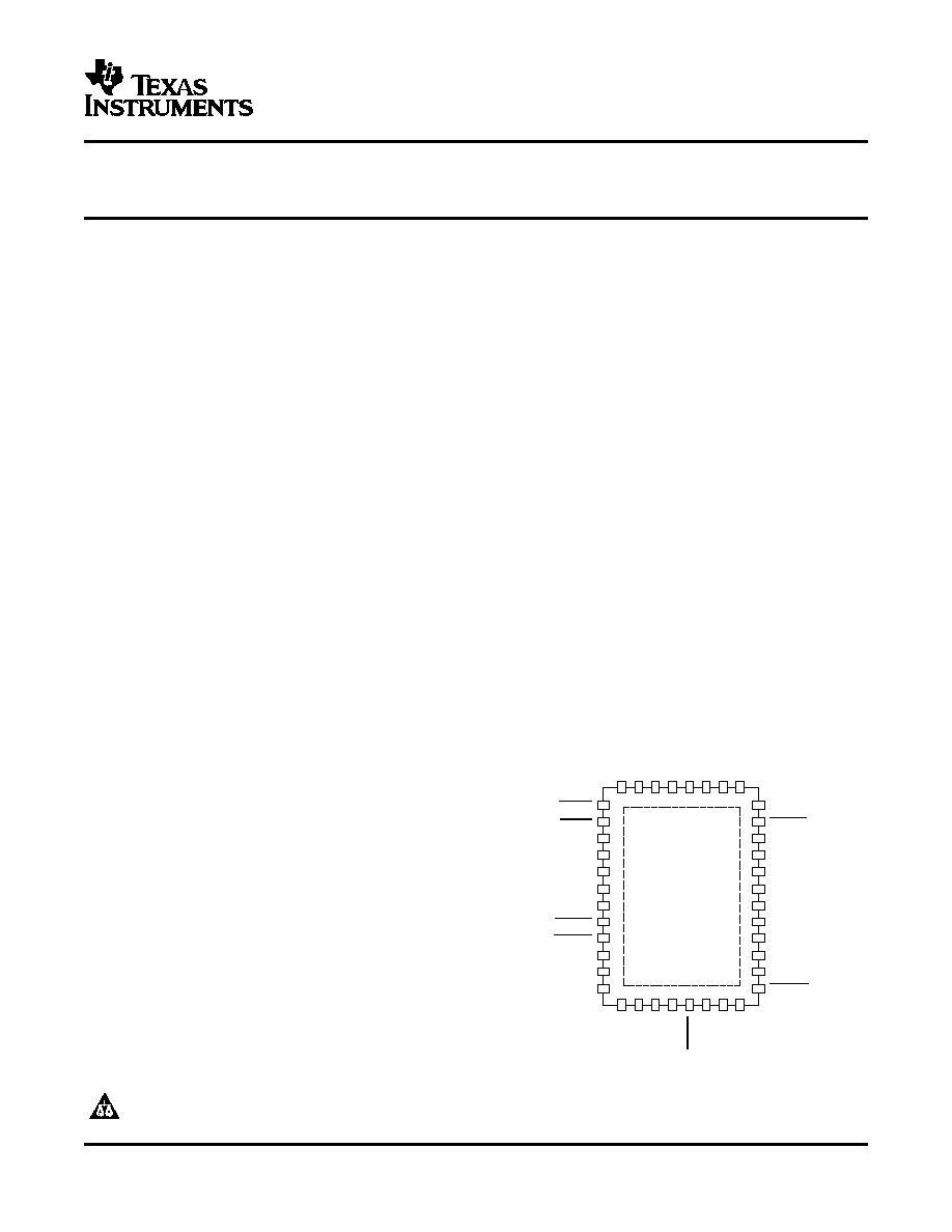
bq24730
(Top View)
CHGEN
ACDRV
ACN
ACP
ACDET
ACSET
BYPASS
FBO
AGND
VREF5
VCC
IADSLP
GND
ACGOOD
ISYNSET
IADAPT
SRN
SRP
SYNN
SYNP
SYS
BATDRV
CELLS
PVCC
BTST
HIDR
V
PH
REGN
LODR
V
PGND
ST
A
T
26
21
AIRDET
EAI
24
DPMDET
23
LBSET
22
EAO
1
2
3
4
5
6
8
7
12
9
10
11
BAT
SRSET
LOWBAT
IBAT
bq24730
SLUS695 MARCH 2006
ADVANCED MULTI-CHEMISTRY AND MULTI-CELL SYNCHRONOUS SWITCH-MODE
CHARGER AND SYSTEM POWER SELECTOR
·
Portable Notebook Computers
·
High Efficiency:
·
Portable DVD Players
NMOS-NMOS Synchronous Buck Converter
·
Webpads, PC Tablets
With Fixed 300 kHz Frequency
Enhanced 6-V Drive Supply Voltage and
99.5% Max Duty Cycle
The bq24730 is a high efficiency synchronous battery
·
High Voltage and Current Regulation
pack charger with high level of integration for portable
Accuracy (0
°
C-85
°
C):
applications.
This
device
implements
a
high
0.4% Charge Voltage Regulation Accuracy
performance analog front-end that interfaces to the
4% Charge Current Regulation Accuracy
system power management micro-controller through
a hardware interface.
4% Adapter Current Regulation Accuracy
Dynamic Power Management (DPM)
The dynamic power management (DPM) function
·
3-Cell or 4-Cell Li-Ion Battery Voltage Select
modifies the charge current depending on system
load conditions, avoiding ac adapter overload.
·
Programmable Battery Charge Current, and
AC Adapter Current via Resistor
High
accuracy
current
sense
amplifiers
enable
accurate measurement of either the charge current or
·
2% Accurate Current Sense Amplifiers for
the ac adapter current, allowing termination of
Both Input Current and Charge Current
nonsmart packs and monitoring of overall system
(0
°
C-125
°
C)
power. The input current sense amplifier can be
·
Input Current Sense Amplifier Can Be Enabled
enabled with no adapter to sense battery discharge
with No Adapter to Sense Battery Discharge
current.
Current
Integrated features such as charger soft start, charge
·
Regulates Charge Current Down to 0-V
overcurrent protection, and IC temperature monitoring
Battery Voltage
provide a second level of protection, in addition to
·
AC Adapter Operating Range 8 V24 V
pack and system protection functions.
·
Internal Soft Start
·
Status Indicators:
AC Adapter Present
Low Battery Indicator
DPM Regulation Loop Active Indicator
·
Reverse Battery to Adapter Discharge
Protection
·
Battery/Adapter to System Power Selector
Function
·
Charge Overcurrent Protection
·
Available in 40-Pin 5x7mm QFN Package
Please be aware that an important notice concerning availability, standard warranty, and use in critical applications of Texas
Instruments semiconductor products and disclaimers thereto appears at the end of this data sheet.
PowerPAD is a trademark of Texas Instruments.
PRODUCTION DATA information is current as of publication date.
Copyright © 2006, Texas Instruments Incorporated
Products conform to specifications per the terms of the Texas
Instruments standard warranty. Production processing does not
necessarily include testing of all parameters.
www.ti.com
DEVICE INFORMATION
bq24730
SLUS695 MARCH 2006
These devices have limited built-in ESD protection. The leads should be shorted together or the device placed in conductive foam
during storage or handling to prevent electrostatic damage to the MOS gates.
ORDERING INFORMATION
BATTERY SHORTED
ORDERING NUMBER
PART NO.
PACKAGE
(VERY LOW BATTERY
QUANTITY
(TAPE AND REEL)
VOLTAGE) OPERATION
bq24730RGFR
3000
40 PIN
bq24730
Charge Current Down to BAT = 0 V
5 x 7 mm QFN
bq24730RGFT
250
PACKAGE THERMAL DATA
TA
40
°
C
DERATING FACTOR
PACKAGE
(1)
JA
POWER RATING
ABOVE T
A
= 25
°
C
RGF
(2)
36
°
C/W
2.36 W
0.028 W/
°
C
(1)
For the most current package and ordering information, see the Package Option Addendum at the end of this document, or see the TI
Web site at
www.ti.com
.
(2)
This data is based on using the JEDEC High-K board and the exposed die pad is connected to a copper pad on the board. This is
connected to the ground plane by a 2
×
3 via matrix.
TERMINAL FUNCTIONS
TERMINAL
DESCRIPTION
NO.
NAME
Charge enable logic level low input. Logic High (HI) on the CHGEN pin disables the charger. Logic Low (LO) on the
1
CHGEN
CHGEN pin enables the charger.
AC adapter to system switch driver output. Connect directly to the gate of the ACFET PMOS power FET. Connect the
FET source to the PVCC node and negative side of the input current-sense resistor. Connect the FET drain to the
system load side. Recommend placing a 10-k
resistor from the gate to the source of the AC FET to keep the FET off
2
ACDRV
when there is no power to the IC. If needed, an optional capacitor from gate to source of the ACFET is used to help
slow down the ON and OFF times. The internal gate drive is asymmetrical allowing a quick turn-off and slower turn-off
in addition to the internal break-before-make logic with respect to the BATDRV.
Adapter current sense resistor, negative input. An optional 0.1-
µ
F ceramic capacitor is placed from this pin to AGND
3
ACN
for common-mode filtering. An optional 0.1-
µ
F ceramic capacitor is placed from ACN to ACP to provide
differential-mode filtering.
Adapter current sense resistor, positive input. Place this on the adapter side of the input current sense resistor.
4
ACP
Recommend placing a 0.1-
µ
F ceramic capacitor from ACP to AGND to provide common-mode filtering.
AC adapter detected sense voltage input. Connect a voltage divider resistor from adapter input (before Bypass FET)
5
ACDET
to ACDET, and another resistor from ACDET to AGND, in order to program adapter detect threshold of 2.4 V. ACDET
threshold should be greater than maximum battery regulation voltage, and lower than the minimum adapter voltage.
AC adapter (input) current limit setting. Program input current limit by a resistor from ACSET to AGND. Input current is
6
ACSET
proportional to the current out of the ACSET pin.
Airline mode program pin. Program airline mode input voltage by a resistor divider between input voltage (before
BYPASS FET) and AGND. VREF5 regulator and system power selector (BYPASS pin and ACDRV pin) are enabled
7
AIRDET
500 ms after AIRDET voltage rises above 1.2 V. Charge is disabled until 500 ms after AIRDET voltage rises above 1.2
V, and 8 ms after ACDET rises above 2.4 V.
Gate drive for the adapter input BYPASS switch to prevent reverse discharge from the battery to the input. Connect
this pin directly to the gate of the input bypass PMOS power FET. The drain of the FET is connected to the adapter
input voltage node. The source of the FET is connected to the positive node of the input current-sense resistor.
8
BYPASS
Recommend placing a 10-k
resistor from the gate to the source of the BYPASS FET to keep the FET off when there
is no power to the IC. An optional capacitor can be placed from the gate to the source to slow-down the switching
times. Adjusting the turn-on and turn-off times is typically not needed for this FET.
Dynamic power management (DPM) input current loop active, open-drain output status. Logic low (LO) indicates input
9
DPMDET
current is being limited by reducing the charge current. A 10-k
pull-up resistor to the host controller supply rail is
needed.
2
Submit Documentation Feedback

www.ti.com
bq24730
SLUS695 MARCH 2006
DEVICE INFORMATION (continued)
TERMINAL FUNCTIONS (continued)
TERMINAL
DESCRIPTION
NO.
NAME
Low battery voltage threshold set. Program depleted battery pack threshold by a resistor from LBSET to AGND. The
10
LBSET
depleted voltage threshold is proportional to the voltage on the LBSET pin.
Error amplifier output for compensation. Connect the feedback compensation components from EAO to EAI. Typically,
11
EAO
a capacitor in parallel with a series resistor and capacitor. See the compensation calculation procedures. This node is
internally compared to the PWM saw-tooth oscillator.
Error amplifier negative input for compensation, also connect the feedback compensation components from EAI to
12
EAI
EAO. Connect the input compensation components from FBO to EAI. See the compensation calculation procedures.
Feedback output for compensation. Connect the input compensation components from FBO to EAI. Typically, a
13
FBO
resistor in parallel with a series resistor and capacitor. See the compensation calculation procedures.
Analog ground. Ground connection for low current sensitive analog and digital signals. Only connect to the PGND and
14
AGND
GND nodes by connecting to the PowerPADTM underneath the IC.
5-V regulated voltage output, used for internal bias. Used to indicate adapter present status, since enabled by AC
15
VREF5
detected. Connect a 1-
µ
F ceramic capacitor from VREF5 pin to AGND as close as possible to the IC .
IC analog positive supply. Connect to adapter input, or diode, or by putting a diode from adapter input and a diode
16
VCC
from battery pack to VCC. Put a 1-
µ
F ceramic capacitor from VCC to AGND, as close as possible to the IC.
Adapter input current sense amplifier sleep mode enable logic input. Logic low (LO) input turns-off the input current
sense amplifier (and enters sleep mode) when the input voltage falls below AIRDET threshold. Logic high (HI) input
17
IADSLP
keeps-on the input current sense amplifier when the input voltage falls below AIRDET threshold and VCC is kept
above 7 V. This allows measuring battery discharge current when the discharge path includes the voltage across
ACP-ACN.
18
GND
Ground. Only connect to the AGND and PGND nodes by connecting to the PowerPADTM underneath the IC.
AC adapter voltage detected and above the AIRDET threshold, open-drain output. Logic high (HI) output indicates
19
ACGOOD
input voltage is above AIRDET threshold. A 10-k
pull-up resistor to the host controller supply rail is needed.
Program current threshold for synchronous to nonsynchronous regulation transition. Place a resistor from ISYNSET to
AGND to program the charge undercurrent threshold to force non-synchronous converter operation at low output
20
ISYNSET
current and prevent negative inductor current. Threshold should be set from inductor current ripple to the full value of
inductor current ripple.
Low battery voltage, open-drain output. Logic low (LO) output on LOWBAT pin indicates the BAT voltage is below the
21
LOWBAT
LBSET depleted battery threshold. A 10-k
pull-up resistor to the host controller supply rail is needed.
Adapter current sense amplifier output. Current sense amplifier output voltage is 20x the current sense resistor
22
IADAPT
differential voltage (ACP-ACN). Place a 0.1-
µ
F capacitor from IADAPT to AGND for filtering the output ripple.
Optionally, add an RC filter after the output capacitor for additional filtering.
Battery charge current sense amplifier output. Current sense amplifier output voltage is 20x the current sense resistor
23
IBAT
differential voltage (SRP-SRN). Place a 0.1-
µ
F capacitor from IBAPT to AGND for filtering the output ripple. Optionally,
add an RC filter after the output capacitor for additional filtering.
Battery charge current limit setting. Program battery charge current limit by a resistor from SRSET to AGND. Battery
24
SRSET
charge current is proportional to the current out of the SRSET pin.
Battery voltage remote sense. Directly connect a kelvin sense trace from the battery pack positive terminal to the BAT
25
BAT
pin to accurately sense the battery pack voltage. Place a 0.1-
µ
F capacitor from BAT to AGND close to the IC to filter
high frequency noise.
Charge current sense resistor, negative input. Connect to the charge current sense resistor negative terminal.
26
SRN
Optionally, add a 0.1-
µ
F ceramic capacitor from SRN to AGND near the IC for common-mode filter.
Charge current sense resistor, positive input. Connect to the charge current sense resistor positive terminal. Placing a
27
SRP
0.1-
µ
F ceramic capacitor from SRP to AGND near the IC for common-mode filter is recommend. Optionally, place a
0.1-
µ
F ceramic capacitor from SRP to SRN near the IC for differential-mode filter.
Charge overcurrent and charge undercurrent negative sense input. Connect to the charge current sense resistor
negative terminal. If sensing the same sense resistor as SRN, the user can connect directly to the SRN pin and no
28
SYNN
further filter capacitors are needed. To sense a different sense resistor, add a 0.1-
µ
F ceramic capacitor from SYNN to
AGND near the IC for common-mode filter.
Charge overcurrent and charge undercurrent negative sense input. Connect to the charge current sense resistor
positive terminal. If sensing the same sense resistor as SRP, the user can connect directly to the SRP pin, and no
29
SYNP
further filter capacitors are needed. To sense a different sense resistor, add a 0.1-
µ
F ceramic capacitor from SYNP to
AGND near the IC for common-mode filter, and place a 0.1-
µ
F ceramic capacitor from SYNP to SYNN near the IC for
differential-mode filter.
30
SYS
System load, voltage sense. Connect directly to the system load node and the drain of the BAT PMOS power FET.
3
Submit Documentation Feedback
www.ti.com
ABSOLUTE MAXIMUM RATINGS
bq24730
SLUS695 MARCH 2006
DEVICE INFORMATION (continued)
TERMINAL FUNCTIONS (continued)
TERMINAL
DESCRIPTION
NO.
NAME
Battery to system switch driver output. Gate drive for the battery to system load BAT PMOS power FET to isolate the
system from the battery to prevent current flow from the system to the battery, while allowing a low impedance path
from battery to system and while discharging the battery pack to the system load. Connect this pin directly to the gate
of the input BAT PMOS power FET. Connect the source of the FET to the system load voltage node. Connect the
31
BATDRV
drain of the FET to the battery pack positive node. Placing a 10-k
resistor from the gate to the source of the BAT
FET to keep the FET off when there is no power to the IC is recommended. An optional capacitor is placed from the
gate to the source to slow-down the switching times. The internal gate drive is asymmetrical allowing a quick turn-off
and slower turn-off in addition to the internal break-before-make logic with respect to the ACDRV.
Battery pack cell select logic input. Logic low (LO) input programs 3-cell Li-Ion output voltage (12.6 V). Logic high (HI)
32
CELLS
input programs 4-cell Li-Ion output voltage (16.8 V)
Charger status, open-drain output. Logic low(LO) output indicates charger is on. Logic high (HI) output indicates
33
STAT
controller is not charging. A 10-k
pull-up resistor to the host controller supply rail is needed.
Power ground. Ground connection for the high-current power converter nodes. Only connect to the AGND and GND
34
PGND
nodes by connecting to the PowerPADTM underneath the IC.
35
LODRV
PWM low side driver output. Connect directly to the gate of the low-side NMOS power FET with a short trace.
Low-side driver gate voltage regulator and source for high-side driver bootstrap voltage. Add a 1-
µ
F ceramic capacitor
36
REGN
from REGN pin to PGND pin, close to the IC. Place a small signal Schottky diode from REGN to BTST for bootstrap
voltage.
Synchronous buck phase node. Connect directly to the source of the high-side NMOS FET with a short trace. This
37
PH
node is the common connection between the high-side FET, low-side FET, and output inductor. Connect a 0.1-
µ
F
boot-strap ceramic capacitor from BTST to PH.
38
HIDRV
PWM high side driver output. Connect directly to the gate of the high-side NMOS power FET with a short trace.
High-side FET Boot-strap input pin. Connect to positive side of boot-strap capacitor. Connect a 0.1-
µ
F bootstrap
capacitor from the BTST pin to the PH node. Also, connect a bootstrap diode with the anode connected to the REGN
39
BTST
pin and the cathode connected to the BTST pin. An optional 4.7-
- 15-
series resistor is placed between the BTST
pin and the bootstrap-diode/capacitor junction to slow-down the turn-on time of the high-side FET for reducing ringing
due to high dv/dt of the phase node.
IC power positive supply. Connect directly to the drain of the high-side NMOS power FET. A 0.1-
µ
F decoupling
40
PVCC
ceramic capacitor is recommended from PVCC to PGND.
over operating free-air temperature range (unless otherwise noted)
(1) (2)
PIN
VALUE / UNIT
ACN, ACP, PVCC, ACDRV, SYNN, SYNP, SRP, SRN , BATDRV,
0.3 V to 30 V
BAT, BYPASS, SYS, VCC
PH
1 V to 30 V
Supply voltage range
LODRV, REGN, FBO, EAI, EAO, ACGOOD, ISYNSET, CHGEN,
VREF5, ACDET, IBAT, STAT, ACSET, AIRDET, DPMDET,
0.3 V to 7 V
LBSET, IADSLP, LOWBAT, IADAPT, SRSET, CELLS
BTST, HIDRV (with respect to AGND and PGND)
1 V to 36 V
Maximum differential voltage
AGND-PGND, AGND-DGND
0.3 V to 0.3 V
Maximum difference voltage
ACPACN , SRPSRN, and SYNPSYNN
0.6 V
Operating ambient temperature range (T
A
)
40
°
C to 85
°
C
Maximum junction temperature (T
J
)
150
°
C
Storage temperature range (T
stg
)
65
°
C to 150
°
C
(1)
Stresses beyond those listed under absolute maximum ratings may cause permanent damage to the device. These are stress ratings
only, and functional operation of the device at these or any other conditions beyond those indicated under recommended operating
conditions is not implied. Exposure to absolute-maximum-rated conditions for extended periods may affect device reliability.
(2)
All voltages are with respect to AGND, unless otherwise noted. Currents are positive into, negative out of the specified terminal. Consult
Packaging Section of the Data book for thermal limitations and considerations of packages.
4
Submit Documentation Feedback
www.ti.com
RECOMMENDED OPERATING CONDITIONS
ELECTRICAL CHARACTERISTICS
bq24730
SLUS695 MARCH 2006
PIN
MIN
NOM
MAX
UNIT
ACN, ACP, PVCC, ACDRV, SRP, SRN, BATDRV, BAT,
0
24
V
BYPASS, SYS, VCC, SYNN, SYNP
PH
0.5
24
V
LODRV, REGN, VREF5
0
6.5
V
Supply voltage range
FBO, EAI, EAO, ACGOOD, ISYNSET, CHGEN, ACDET, STAT,
ACSET, AIRDET, DPMDET, LBSET, IADSLP, LOWBAT,
0
5.5
V
SRSET, CELLS, IBAT, IADAPT, ACDET
BTST, HIDRV
0
30
V
Maximum differential voltage
AGND-PGND, AGND-DGND
0
V
Maximum difference voltage
ACPACN, SYNNSYNP, SRPSRN
0.5
V
Junction temperature range (T
J
)
-40
125
°
C
Storage temperature range (T
stg
)
-55
150
°
C
8 Vdc
V
(VCC)
24 Vdc, 0
°
C
T
J
125
°
C, all voltages with respect to AGND (unless otherwise noted)
PARAMETER
TEST CONDITIONS
MIN
TYP
MAX
UNIT
BATTERY VOLTAGE REGULATION
V
(BAT_ICR)
VBAT Input voltage range
V
(BAT)
0
PVCC
V
T
J
= 0
°
C 85
°
C
0.4%
0.4%
Battery regulation voltage Accuracy
12.6 V and 16.8 V
T
J
= 0
°
C 125
°
C
0.5%
0.5%
CELLS = 0
12.6
V
(VBATREG)
BAT voltage regulation range
V
CELLS = 1
16.8
PWM AC ADAPTER INPUT CURRENT REGULATION, DPM (DYNAMIC POWER MANAGEMENT)
ACP-ACN differential voltage range
V
(IREG_DPM)
V
(IREG_DPM)
= V
(ACP)
- V
(ACN)
200
mV
for input current regulation
V
(ACSET)
Voltage on the ACSET pin
1
V
G
(ACSET)
ACSET gain
1000
V/A
V
(ACP)
V
(ACN)
= 40 mV
3%
4%
(4 A with 10 m
)
T
J
= 0
°
C 85
°
C, V
CC
V
CC
(min),
V
CC
V
(BAT)
+ V
(DO-MAX)
,
(1)
V
(ACP)
V
(ACN)
= 20 mV
Current regulation accuracy
Over differential threshold range, V
(IREG)
,
3%
7%
(2 A with 10 m
)
Does not include error induced by the
tolerance of the sense resistor, R
(SNS)
V
(ACP)
V
(ACN)
= 5 mV
25%
25%
(0.5 A with 10 m
)
PWM BATTERY CHARGE CURRENT REGULATION
SRP-SRN differential voltage range
V
(IREG_CHG)
V
(IREG_CHG)
= V
(SRP)
- V
(SRN)
200
mV
for input current regulation
V
(SRSET)
Voltage on the SRSET pin
1
V
G
(SRSET)
SRSET gain
1000
V/A
V
(SRP-SRN)
= 40 mV
3%
4%
(4 A with 10 m
)
T
J
= 0
°
C 85
°
C, V
CC
V
CC
(min),
V
CC
V
(BAT)
+ V
(DO-MAX)
,
(1)
V
(SRP-SRN)
= 20 mV
Current regulation accuracy
Over differential threshold range, V
(IREG)
,
3%
7%
(2 A with 10 m
)
Does not include error induced by the
tolerance of the sense resistor, R
(SNS)
V
(SRP-SRN)
= 5 mV
25%
25%
(0.5 A with 10 m
)
CHARGE CURRENT SENSE AMPLIFIER IBAT AMPLIFIER
SRP, SRN common-mode input
2.5
20
V
voltage range
V
(IBAT)
V
(IBAT)
= V
(SRP, SRN)
×
G
(IBAT)
IBAT output voltage range
0
3.5
V
V
(BAT)
> 2.5 V or V
(BAT)
> V
(IBAT)
+ V
(DO-MAX)
(1)
G
(IBAT)
Voltage gain
G
(IBAT)
= V
(IBAT)
/ V
(SRP, SRN)
20
V/V
V
(SRP-SRN)
= 40 mV
2%
2%
(4 A with 10 m
)
Charge current sense amplifier output
V
(BAT)
> 2.5 V or V
(BAT)
>
V
(SRP-SRN)
= 20 mV
3%
3%
voltage accuracy
V
(IBAT)
+ V
(DO-MAX)
(1)
(2 A with 10 m
)
V
(SRP-SRN)
= 5 mV
25%
25%
(0.5 A with 10 m
)
I
(BAT_LIM)
IBAT output current limit
IBAT shorted to AGND
4.5
mA
(1)
V
(DO-max)
is defined as the maximum drop-out voltage. V
(DO-max)
= 1 V unless other wise specified. In an actual application, V
(DO - MAX)
=
(R
(SNS)
×
I
O
) + V
(DSON_HIGH_SIDE_FET)
+ V
(DSON_BYPASS_FET)
.
5
Submit Documentation Feedback
Document Outline