bq24901 Single-Cell Li-Ion and Li-Pol Charge Management IC

bq24901
SLUS527 DECEMBER 2002
SINGLE CELL LI ION AND LI POL CHARGE MANAGEMENT IC
FOR OFFLINE APPLICATIONS
1
www.ti.com
FEATURES
D
Designed for Off-Line Charger Design for
Single-Cell Li-Ion Packs
D
Provides Control Feedback to a Primary-Side
Controller
D
Robust Battery Insertion and Removal
Detection
D
Charge Current and Voltage Regulation
Feedback to Primary-Side for High-Accuracy
Charging
D
Charge Termination by Minimum Current and
Time
D
Pre-Charge Conditioning Regulator with
Safety Timer
D
Charge Status Outputs for LED or Host
Processor Interface Indicates Charge-
in-Progress, Charge Completion, and Fault
Conditions
D
Temperature Monitoring Before and During
Charge
D
Short-Circuit Protection
D
Small, 14-Pin TSSOP Package
APPLICATIONS
D
Cradle Chargers for Digital Cameras
D
Desktop Chargers
D
Handheld Devices
DESCRIPTION
The bq24901 Li-Ion charge management devices
are designed specifically for off-line charger
applications. The bq24901 resides on the
secondary-side of the transformer and provides
the control feedback to a variety of primary side
controllers. The bq24901 offers current or voltage
regulation feedback, temperature monitoring,
charge status, and adjustable charge termination,
in a single monolithic device. During
battery-absent or charge-complete conditions,
the bq24901 continuously regulates the
secondary-side voltage, used as V
CC
supply to
the device.
The bq24901 features a time-limited precon
ditioning phase to condition deeply discharged
cells. The pre-conditioning phase is achieved by
linear regulation in the secondary side. Following
preconditioning, the bq24901 regulates the
charge current to the value set by the external
current sense resistor. Once the battery reaches
the charge voltage, the voltage regulation loop
takes over and completes the charge cycle. The
accuracy of the voltage regulation is better than
±
30mV. Charge is terminated based on minimum
current. The minimum current level is set through
TADJ pin. An internal five-hour charge timer
provides a backup for charge termination.
The bq24901 is designed to reliably detect battery
insertion and removal conditions, including packs
with open protectors. Other standard features
include a recharge feature activated when the
battery voltage falls below the V
RCH
threshold.
PRODUCTION DATA information is current as of publication date.
Products conform to specifications per the terms of Texas Instruments
standard warranty. Production processing does not necessarily include
testing of all parameters.
Copyright
2002, Texas Instruments Incorporated
bq24901
SLUS527 DECEMBER 2002
2
www.ti.com
DESCRIPTION (continued)
In addition to the standard features, the bq24901 offers battery temperature monitoring and status display. The
temperature-sense circuit continuously measures battery temperature using an external thermistor and
suspends charge until the battery temperature is within the userdefined thresholds. The STAT pins indicate
conditions of operation of the charger. These outputs can be used to drive an LED or interface to a host
microcontroller.
These devices have limited built-in ESD protection. The leads should be shorted together or the device placed in conductive foam
during storage or handling to prevent electrostatic damage to the MOS gates.
ORDERING INFORMATION
TA
CHARGE REGULATION
VOLTAGE
PACKAGE DEVICES(1)
TOP SIDE MARKINGS
20
°
C to 85
°
C
4.2 V
bq24901PW
bq24901
(1) The PW package is also available taped and reeled. Add an R suffix to the device type (i.e., bq24901PWR) for quantities of 2,500 devices per
reel.
PACKAGE DISSIPATION RATING TABLE
PACKAGE
JA
TA
25
°
C
POWER RATING
DERATING FACTOR
ABOVE TA = 25
°
C
PW
110
°
C/ W
907 mW
9.07 mW/
°
C/
ABSOLUTE MAXIMUM RATINGS
over operating free-air temperature range unless otherwise noted(1)
bq24901
UNIT
Supply voltage, VCC
with respect to VSS
11.5
V
I
t
lt
V
SNS, BAT, STAT1, STAT2, VCOMP, ICOMP, SCOMP, OPTD, CC
(all with respect to Vss)
11.5
V
Input voltage range, VI
TADJ, VREF (all with respect to Vss)
7
V
TS (with respect to Vss)
0.3 to VCC + 0.3 V
Output sink/source current, IO
STAT1, STAT2, OPTD
20
O tp t sink c rrent
CC
80
mA
Output sink current
VREF
1
mA
Operating free-air temperature range, TA
40 to 100
Junction temperature range, TJ
40 to 125
°
C
Storage temperature, Tstg
65 to 150
°
C
Lead temperature 1,6 mm (1/16 inch) from case for 10 seconds
300
(1) Stresses beyond those listed under "absolute maximum ratings" may cause permanent damage to the device. These are stress ratings only,
and functional operation of the device at these or any other conditions beyond those indicated under "recommended operating conditions" is
not implied. Exposure to absolute-maximum-rated conditions for extended periods may affect device reliability.
RECOMMENDED OPERATING CONDITIONS
MIN
MAX
UNIT
Supply voltage, VCC
3
10
V
Operating free-air temperature, TA
20
85
°
C

bq24901
SLUS527 DECEMBER 2002
3
www.ti.com
ELECTRICAL CHARACTERISTICS
Over recommended operating free-air temperature and supply voltage (unless otherwise noted)
PARAMETER
TEST CONDITIONS
MIN
TYP
MAX
UNIT
SUPPLY CURRENT
ICC(VCC)
Input current
VCC > VCC(min)
2
mA
IIB(BAT)
Input bias current on BAT pin
VI(BAT) > VO(REG), when not in charge
1
IIB(TS)
Input bias current on TS pin
VI(TS) = 2.5 V
1
A
IIB(SNS)
Input bias current on SNS pin
VCC = 6 V, VI(SNS) = 6 V when not in charge
1
µ
A
IIB(TADJ)
Input bias current on TADJ pin
VI(TADJ) = VREF
1
BATTERY VOLTAGE and VCC REGULATION
VO(REG)
Output voltage
0
°
C
TA
70
°
C
4.17
4.20
4.23
V
VCC
Supply voltage
5.8
6.0
6.3
V
CURRENT REGULATION
V(SNS)
Current regulation threshold
voltage
Voltage at pin SNS relative to BAT,
0
°
C
TA
70
°
C,
V(LOWV)
V(SNS)
VO(REG)
184
200
216
mV
Input common mode range on
SNS pin
V(UVT)
VCC
V
PRE-CHARGE AND SHORT-CIRCUIT CURRENT REGULATION
Pre-charge voltage threshold
Voltage at pin SNS relative to BAT pin,
0
°
C
TA
70
°
C
V(UVT)
VI(BAT)
V(LOWV)
10
20
30
mV
ISC
Short-circuit current
0
°
C
TA
70
°
C, 0
VI(BAT)
V(UVT)
5.4
30.0
mA
CHARGE TERMINATION DETECTION
V
Charge termination current detect
Voltage at pin SNS relative to BAT pin,
0
°
C
TA
70
°
C
TADJ pin tied to VREF pin,
VI(SNS) = VO(REG)VI(BAT) > V(RCH)
16
20
24
mV
V(ITERM)
Charge termination current detect
threshold
Voltage at pin SNS relative to BAT pin,
0
°
C
TA
70
°
C
TADJ pin tied to VSS pin,
VI(SNS) = VO(REG)VI(BAT) > V(RCH)
7.5
10.0
12.5
mV
V(EN-TERM) Enable termination voltage
(VI(SNS) VI(BAT)
)
< V(ITERM) , VBAT increasing
above threshold
VO(REG)
210
VO(REG)
160
VO(REG)
110
V
t(TRMDET2)
Falling-edge delay for termination
detection
(VSNS VBAT
)
increasing above threshold,
VI(BAT) > V(ENTERM),
100 ns fall time
2 mV overdrive
100
µ
s
t(TRMDET1)
Rising-edge delay for termination
detection
(VSNS VBAT
)
increasing above threshold,
VI(BAT) > V(ENTERM),
100 ns fall time
2 mV overdrive
20
ms
TEMPERATURE COMPARATOR
V(LTF)
Cold temperature threshold voltage
VTS,
VCC
3.5 V
72.6
73.5
74.1
V(HTF)
Hot temperature threshold voltage
VTS,
VCC
3.5 V
33.7
34.4
35.1
%V
V(TCO)
Cutoff temperature threshold voltage
VTS,
VCC
3.5 V
28.7
29.3
29.9
%VCC
LTF hysteresis
Hysteresis for LTF threshold voltage
0.1
0.6
1.1
LOW BATTERY VOLTAGE (LOWV) THRESHOLD COMPARATOR
V(LOWV)
3.00
3.05
3.15
V
(1)
Ensured by design. Not production tested.

bq24901
SLUS527 DECEMBER 2002
4
www.ti.com
ELECTRICAL CHARACTERISTICS (continued)
Over recommended operating free-air temperature and supply voltage (unless otherwise noted)
PARAMETER
UNIT
MAX
TYP
MIN
TEST CONDITIONS
BATTERY RECHARGE THRESHOLD (VRCH) COMPARATOR
V(RCH)
Recharge threshold voltage
VO(REG)
0.24
VO(REG)
0.12
V
POWER-ON RESET (POR)
V(POR)
POR threshold voltage
2.60
2.70
2.85
V
TIMERS
t(PRECHG) Precharge time
VI(BAT) < V(LOWV)
1,350
1,800
2,250
t(CHG)
Charge time
V(LOWV) < VI(BAT) < VO(REG),
(VI(SNS) VI(BAT)
)
< V(ITERM)
13,500
18,000
22,500
s
OPTO-DRIVER PIN (OPTD)
VSAT(OPTD) Output saturation voltage
IO(OPTD) = 10 mA
100
mV
I(OPTDLKG) Opto-driver leakage current
V(OPTD) = 5 V,
VI(BAT) < VO(REG)
VCC = 5.8 V,
(VI(SNS) VI(BAT)
)
< 184 mV
100
µ
A
gM
Transconductance
IO(OPTD) = 5 mA
5
500
S
Gain-bandwidth product
IO(OPTD) = 5 mA, RLOAD = 100
1
MHz
DISCHARGE CURRENT, DISCHARGE VOLTAGE, CONDITION CURRENT AND WAKE CURRENT
I(DISCHG)
Discharge current
1 V
VI(BAT)
4.2 V
60
300
800
µ
A
t(DISCHG1) Discharge time 1
250
310
370
ms
t(DISCHG2) Discharge time 2
20
25
30
ms
V(DISCHG) Discharge voltage(1)
1.5
2.0
2.5
V
I
Batter detection c rrent
I(DETECT_min) at VCC = 5.8 V,VI(BAT) = 4.2 V
0.8
I(DETECT)
Battery detection current
I(DETECT_max) at VCC = 6 V, VI(BAT) = 0 V
30
mA
I
Wake current source 1
I(WK_SRC_min) at VCC = 5.8 V,VI(BAT) = 4.2 V
0.8
mA
I(WK_SRC) Wake current, source 1
I(WK_SRC_max) at VCC = 6 V,VI(BAT) = 0 V
30
I
Wake c rrent so rce 2
I(WK_SINK_min) at VCC = 5.8 V,VI(BAT) = 4.2 V
0
A
I(WK_SINK) Wake current, source 2
I(WK_SINK_max) at VCC = 6 V,VI(BAT) = 0 V
1000
µ
A
t(WK)
Wake time
100
125
150
ms
CHARGE STATUS OUTPUT (STAT1/STAT2)
VOL(STATx) Low-level output saturation voltage
IO(STATx) = 10 mA, VCC
3.5 V
0.5
V
VOLTAGE REFERENCE OUTPUT (VREF)
VREF voltage threshold
0 V < IO(VREF) < 500
µ
A, 0
°
C
TA
70
°
C
1.18
1.22
V
CHARGE CONTROL OUTPUT (CC)
VOL
Low-level output voltage (FstChg)
IO(CC) = 40 mA (sink)
0.45
V
COUT
Output capacitance
LDO to BAT,
LDO to VSS
0.1
10.0
µ
F
UNDERVOLTAGE THRESHOLD SHORT-CIRCUIT PROTECTION
V(UVT)
Undervoltage threshold voltage
2.00
2.15
V
(1)
Ensured by design. Not production tested.
bq24901
SLUS527 DECEMBER 2002
5
www.ti.com
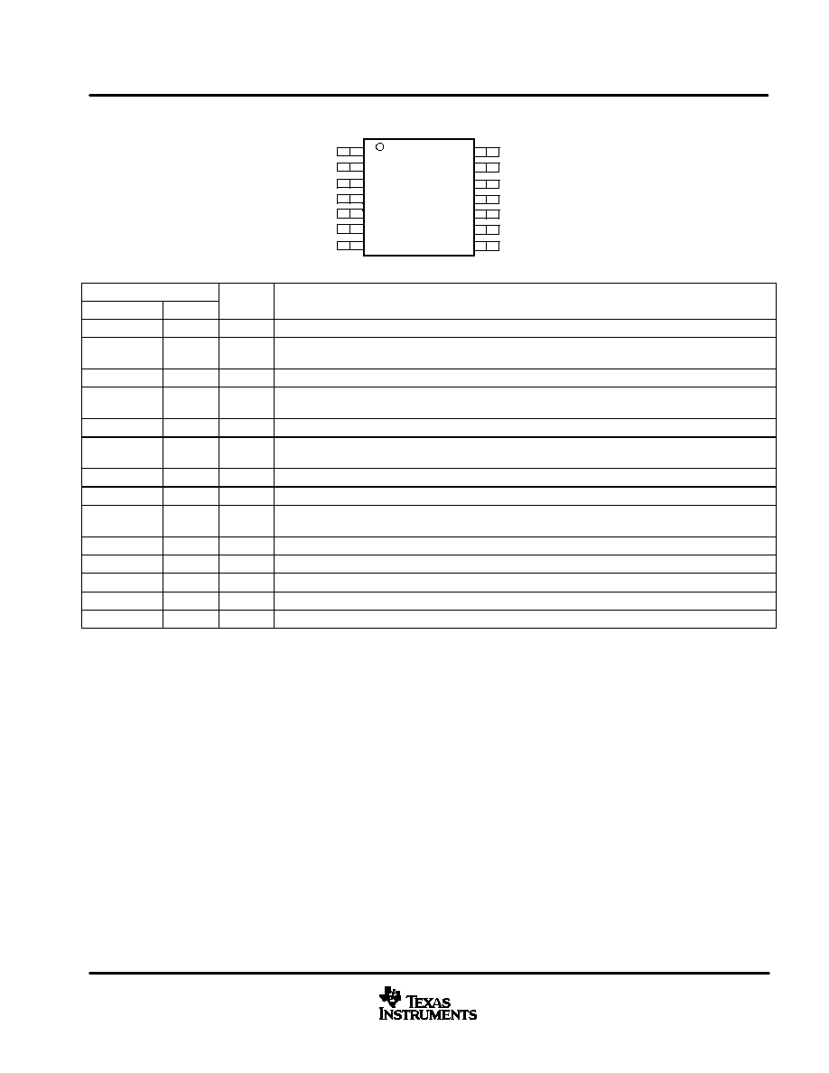
1
2
3
4
5
6
7
14
13
12
11
10
9
8
OPTD
VCC
SCOMP
ICOMP
VCOMP
STAT1
STAT2
VSS
CC
SNS
BAT
TS
VREF
TADJ
PW PACKAGE
(TOP VIEW)
TERMINAL FUNCTIONS
TERMINAL
I/O
DESCRIPTION
NAME
NO.
I/O
DESCRIPTION
BAT
11
I
Battery voltage sense input. This input is tied directly to the positive side of the battery pack.
CC
13
O
Charge control output. CC is an open-drain pulldown output that is used to drive an external pass tran-
sistor for charge current and voltage control
ICOMP
4
I
Current loop compensation. This is the compensation for the fast charge current regulation loop.
OPTD
1
O
Optocoupler driver output. This open-collector output is used to provide feedback to the primary side
by driving an external optocoupler.
SCOMP
3
I
Supply loop compensation. This is the compensation for the VCC supply regulation loop.
SNS
12
I
Current sense input. Battery current is sensed via the voltage developed on this pin by an external
sense resistor.
STAT1
6
O
Charge status output 1 (open drain)
STAT2
7
O
Charge status output 2 (open drain)
TADJ
8
I
Termination adjust. This input is used to set the minimum current termination level during voltage regu-
lation phase.
TS
10
I
Temperature sense Input. Input for an external battery temperature monitoring.
VCC
2
I
VCC supply input.
VCOMP
5
I
Voltage loop compensation. This is the compensation for the battery regulation loop
VREF
9
O
Voltage reference output. This buffered output provides the internal bandgap voltage.
VSS
14
Ground input.
Document Outline
- FEATURES
- APPLICATIONS
- DESCRIPTION
- ORDERING INFORMATION
- PACKAGE DISSIPATION RATING TABLE
- ABSOLUTE MAXIMUM RATINGS
- RECOMMENDED OPERATING CONDITIONS
- ELECTRICAL CHARACTERISTICS
- TERMINAL FUNCTIONS
- FUNCTIONAL BLOCK DIAGRAM
- APPLICATION INFORMATION
- Charge Qualification and Pre-Conditioning
- Temperature Sense (TS) Input
- VCC Regulation
- Voltage Monitoring and Regulation
- Current Regulation
- Current Regulation Ramp-Up and Ramp-Down
- Battery Insertion and Removal Detection
- Charge Termination and Re-Charge
- Charge Timers
- Charge Status Display
- IMPORTANT NOTICE