Single Chip Charger and DC/DC Converter IC for Bluetooth (bqHYBRID) (Rev. A)
www.ti.com
FEATURES
DESCRIPTION
APPLICATIONS
5
6
7
8
19
3
AC
USB
SW
VSS
STAT1
STAT2
13
12
ISET2
ISET1
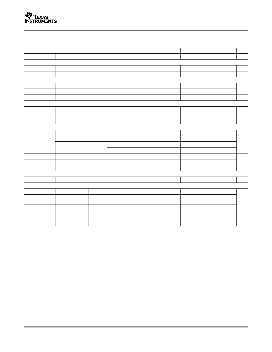
bq25012RHL
PACK+
PACK-
VDC
GND
VBUS
GND
D+
D -
USB Port
AC Adapter
15
CE
2
FB
16
BAT/OUT
+
DSP
Processor
Bluetooth Chipset
Battery
Pack
1.8 V
17
BAT/OUT
9
18
VSS
VSS
EN
4
20
FPWM
UDG-04070
R
SET
14
PG
bq25010
bq25011
bq25012
SLUS615A DECEMBER 2004 REVISED MARCH 2005
SINGLE-CHIP CHARGER AND DC/DC CONVERTER IC FOR BLUETOOTH HEADSETS
AND OTHER PORTABLE APPLICATIONS (bq2501x)
·
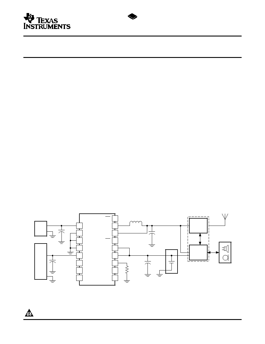
Li-Ion Or Li-Pol Charge Management and
The bq2501x series are highly integrated charge and
Synchronous DC-DC Power Conversion In a
power management devices targeted at space-limited
Single Chip
bluetooth applications. The bq2501x series offer inte-
grated power FET and current sensor for charge
·
Optimized for Powering Bluetooth Headsets
control, reverse blocking protection, high accuracy
and Accessories
current and voltage regulation, charge status, charge
·
Charges and Powers the System from Either
termination, and a highly efficient and low-power
the AC Adapter or USB with Autonomous
dc-dc converter in a small package.
Power Source Selection
The bq2501x charges the battery in three phases:
·
Integrated USB Charge Control with
conditioning, constant current and constant voltage.
Selectable 100 mA and 500 mA Charge Rates
Charge is terminated based on minimum current. An
·
Integrated Power FET and Current Sensor for
internal charge timer provides a backup safety feature
for charge termination. The bq2501x automatically
Up to 500 mA Charge Applications AND
re-starts the charge if the battery voltage falls below
100 mA 1.8 V DC-DC Controller with
an internal threshold. The bq2501x automatically
Integrated FET
enters sleep mode when V
CC
supply is removed.
·
Reverse Leakage Protection Prevents Battery
The integrated low-power high-efficiency dc-dc con-
Drainage
verter
is
designed
to
operate
directly
from
a
·
Automatic Power Save Mode For High
single-cell Li-Ion or Li-Pol battery pack. The output
Efficiency at Low Current, or Forced PWM for
voltage is either adjustable from 0.7 V to VBAT
Frequency Sensitive Applications
(bq25010), fixed at 3.3 V (bq25011), or fixed at 1.8 V
(bq25012), and is capable of delivering up to 150-mA
of load current. The dc-dc converter operates at a
synchronized 1 MHz switching frequency allowing for
·
Bluetooth Headsets
the use of small inductors.
·
Bluetooth Accessories
·
Low-Power Handheld Devices
TYPICAL APPLICATION
Please be aware that an important notice concerning availability, standard warranty, and use in critical applications of Texas
Instruments semiconductor products and disclaimers thereto appears at the end of this data sheet.
UNLESS OTHERWISE NOTED this document contains PRO-
Copyright © 20042005, Texas Instruments Incorporated
DUCTION DATA information current as of publication date. Prod-
ucts conform to specifications per the terms of Texas Instruments
standard warranty. Production processing does not necessarily
include testing of all parameters.
www.ti.com
ABSOLUTE MAXIMUM RATINGS
(1)
RECOMMENDED OPERATING CONDITIONS
DISSIPATION RATINGS
bq25010
bq25011
bq25012
SLUS615A DECEMBER 2004 REVISED MARCH 2005
These devices have limited built-in ESD protection. The leads should be shorted together or the device
placed in conductive foam during storage or handling to prevent electrostatic damage to the MOS gates.
ORDERING INFORMATION
(1)
PACKAGE
T
A
OUTPUT VOLTAGE (V)
PART NUMBER
(2) (3)
MARKING
Adjustable
bq25010RHLR
ANC
-40°C to 125°C
3.3
bq25011RHLR
(4)
ANE
1.8
bq25012RHLR
ANF
(1)
For the most current package and ordering information, see the Package Option Addendum at the end of this document, or see the TI
website at
www.ti.com
(2)
The RHL package is available taped and reeled only in quantities of 3,000 devices per reel.
(3)
This product is RoHS compatible, including a lead concentration that does not exceed 0.1% of total product weight, and is suitable for
use in specified lead-free soldering processes. In addition, this product uses package materials that do not contain halogens, including
bromine (Br) or antimony (Sb) above 0.1% of total product weight.
(4)
Advanced Information, contact factory for availability.
over operating free-air temperature range (unless otherwise noted)
bq25010
bq25011
bq25012
Supply voltage
AC, USB (wrt VSS)
0.3 V to 7 V
PG, OUT, ISET1, ISET2, STAT1, STAT2, TS (wrt VSS)
0.3 V to 7 V
Input voltage
EN, FB, FPWM, SW (wrt VSS)
V
OUT
+ 0.3 V
PG, STAT1, STAT2
15 mA
Output sink/source current
TS
200 µA
Output source current
OUT
1.5 A
Storage temperature range, T
stg
65°C to 150°C
Junction temperature range, T
J
0°C to 125°C
Lead temperature (solderig, 10 seconds)
260°C
ESD rating (human body model, HBM)
1500 V
(1)
Stresses beyond those listed under absolute maximum ratings may cause permanent damage to the device. These are stress ratings
only, and functional operation of the device at these or any other conditions beyond those indicated under recommended operating
conditions is not implied. Exposure to absolute-maximum-rated conditions for extended periods may affect device reliability. All voltage
values are with respect to the network ground terminal unless otherwise noted.
MIN
MAX
UNIT
V
CC
Supply voltage (from AC input)
4.5
6.5
V
V
CC
Supply voltage (from USB input)
4.35
6.5
T
J
Operating junction temperature range
40
125
°C
T
A
< 40°C
DERATING FACTOR
PACKAGE
JA
POWER RATING
ABOVE T
A
= 40°C
20-pin RHL
(1)
1.81 W
21 mW/°C
46.87°C/W
(1)
This data is based on using the JEDEC High-K board and the exposed die pad is connected to a Cu pad on the board. This is
connected to the ground plane by a 2×3 via matrix.
2
www.ti.com
ELECTRICAL CHARACTERISTICS
bq25010
bq25011
bq25012
SLUS615A DECEMBER 2004 REVISED MARCH 2005
over junction temperature range (0°C
T
J
125°C) and the recommended supply voltage range (unless otherwise noted)
PARAMETER
TEST CONDITIONS
MIN
TYP
MAX UNIT
INPUT CURRENT
I
CC(VCC)
Supply current 1, VCC
V
VCC
> V
VCC(min)
1.2
2.0
mA
Sum of currents into OUT/BAT,
I
CC(SLP)
Sleep current
2
5
V
VCC
< V
(SLP)
I
CC(STDBY)
Standyby current
CE = High, 0°C
T
J
85°C
150
µA
Charge DONE, V
VCC
> V
VCC(min)
,
I
IB(OUT)
Input current, OUT
15
35
I
OUT(SW)
= 0 mA, Converter not switching
I
IB
Input current, CE
1
CHARGE VOLTAGE REGULATION (V
BAT(REG)
+ V
(DO-MAX)
V
VCC
, I
(TERM)
< I
OUT(BAT)
0.5 A)
V
REG(BAT)
Charger output voltage
4.2
V
T
A
= 25°C
0.35%
0.35%
Charge voltage regulation
accuracy
1%
1%
(V
(AC)
V
(OUT)
)
AC dropout voltage
V
OUT (BAT)
= V
REG (BAT)
, I
OUT(BAT)
= 0.5 A
175
250
V
OUT (BAT)
= V
REG (BAT)
, ISET2 = High
350
500
mV
(V
(USB)
V
(OUT)
)
USB dropout voltage
V
OUT (BAT)
= V
REG (BAT)
, ISET2 = Low
60
100
CHARGE CURRENT REGULATION
V
VCC
4.5 V, V
OUT (BAT)
= V
(LOWV)
,
I
OUT (BAT)
AC output current range
V
VCC
V
OUT (BAT)
> V
(DO-MAX)
,
50
500
I
OUT(BAT)
= (K
(SET)
× V
(SET)
/ R
SET
)
V
VCC(min)
4.5 V, V
OUT (BAT)
= V
(LOWV)
,
mA
80
100
V
VCC
V
OUT (BAT)
> V
(DO-MAX)
, ISET2= Low
I
OUT (BAT)
USB output current range
V
VCC(min)
4.5 V, V
OUT (BAT)
= V
(LOWV)
,
400
500
V
VCC
V
OUT (BAT)
> V
(DO-MAX)
, ISET2 = High
Voltage on ISET1, V
VCC
4.5 V,
V
(SET)
Output current set voltage
V
OUT (BAT)
= V
(LOWV)
,
2.436
2.500
2.538
V
V
VCC
V
OUT (BAT)
> V
(DO-MAX)
, ISET2 = High
50 mA
I
OUT(OUT)
500 mA
307
322
337
K
(SET)
Output current set factor
10 mA
I
OUT(OUT)
50 mA
296
320
346
10 mA
I
OUT(OUT)
10 mA
246
320
416
PRECHARGE and SHORT-CIRCUIT CURRENT REGULATION
Precharge to fast-charge tran-
V
(LOWV)
Voltage on OUT/BAT
2.8
3.0
3.2
V
sition threshold
V
VCC(min)
4.5 V, t
FALL
= 100 ns,
Deglitch time for fast-charge to
t
PRECHG_DG
10 mV overdrive,
250
375
500
ms
precharge transition
V
IN(BAT)
decreasing below threshold
0 V < V
IN(BAT)
< V
(LOWV)
, t < t
(PRECHG)
,
I
OUT(PRECHG)
Precharge range
5
100
mA
I
OUT(PRECHG)
= (K
(SET)
× V
(PRECHG)
)/ R
SET
Voltage on ISET1, V
REG(BAT)
= 4.2 V,
V
(PRECHG)
Precharge set voltage
0 V < V
IN(BAT)
< V
(LOWV)
,
240
255
270
mV
t < t
(PRECHG)
CHARGE TAPER and TERMINATION DETECTION
V
IN(BAT)
> V
(RCH)
, t < t
(PRECHG)
,
I
(TAPER)
Charge taper detection range
5
100
mA
I
(TAPER)
= (K
(SET)
× V
(TAPER)
)/ R
SET
Charge taper detection set
Voltage on ISET1, V
REG(BAT)
= 4.2 V,
V
(TAPER)
235
250
265
voltage
V
IN(BAT)
> V
(RCH)
, t < t
(PRECHG)
mV
Voltage on ISET1, V
REG(BAT)
= 4.2 V,
Charge termination detection
V
(TERM)
V
IN(BAT)
> V
(RCH)
, t < t
(PRECHG)
,
11
18
25
set voltage
I
(TERM)
= (K
(SET)
× V
(TERM)
)/ R
SET
3
www.ti.com
bq25010
bq25011
bq25012
SLUS615A DECEMBER 2004 REVISED MARCH 2005
ELECTRICAL CHARACTERISTICS (continued)
over junction temperature range (0°C
T
J
125°C) and the recommended supply voltage range (unless otherwise noted)
PARAMETER
TEST CONDITIONS
MIN
TYP
MAX UNIT
V
VCC(min)
4.5 V, t
FALL
= 100 ns,
Deglitch time for taper detec-
t
TPRDET_DG
10 mV overdrive, I
CHG
increasing above or
250
375
500
tion
decreasong below threshold
ms
V
VCC(min)
4.5 V, t
FALL
= 100 ns,
Deglitch time for termination
t
TERMDET_DG
10 mV overdrive,
350
375
500
detection
I
CHG
decreasing below threshold
BATTERY RECHARGE THRESHOLD
V
REG(BAT)
V
REG(BAT)
V
REG(BAT)
V
RCH
Recharge threshold voltage
V
0.115
0.10
0.085
V
VCC(min)
4.5 V, t
FALL
= 100 ns,
Deglitch time for recharge de-
t
RCHDET
10 mV overdrive, I
CHG
decreasing below or
250
375
500
ms
tect
increasing above threshold
STAT1, STAT2 and PG OUTPUTS
V
OL
Low-level output voltage
I
OL
= 5 mA
0.25
V
ISET2 and CE INPUTS
V
IL
Low-level input voltage
I
IL
= 10 µA
0
0.4
V
V
IH
High-level input voltage
I
IL
= 20 µA
1.4
I
IL
Low-level input current, CE
1
I
IH
High-level input current, CE
1
I
IL
Low-level input current, ISET2
V
ISET2
= 0 V
20
µA
I
IH
High-level input current, ISET2 V
ISET2
= V
CC
40
I
IHZ
High-Z input current, ISET2
V
ISET2
= High-Z
1
TIMERS
t
(PRECHG)
Precharge time
1620
1800
1930
t
(TAPER)
Taper time
1620
1800
1930
s
t
(CHG)
Charge time
16200
18000
19300
I
(FAULT)
Timer fault recovery current
200
µA
SLEEP COMPARATOR for CHARGER
V
VCC
V
(SLP)
Sleep mode entry threshold
2.3 V
V
IN(BAT)
V
REG(BAT)
V
IN(BAT)
+80 mV
V
V
VCC
V
(SLP_DG)
Sleep mode exit threshold
2.3 V
V
IN(BAT)
V
REG(BAT)
V
IN(BAT)
+190 mV
V
CC
decreasing below threshold,
t
(DEGL)
Deglitch time for sleep mode
250
375
500
ms
t
FALL
= 100 ns, 10 mV overdrive,
THERMAL SHUTDOWN
Thermal trip threshold tem-
T
(SHTDWN)
165
perature
°C
Thermal hysteresis
15
UNDERVOLTAGE LOCKOUT AND POR
Undervoltage lockout
V
(UVLO_CHG)
Decreasing V
CC
2.4
2.5
2.6
V
threshold voltage
Hysteresis
27
mV
V
POR
POR threshold voltage
(1)
2.3
2.4
2.5
V
DC-DC INPUT/OUTPUT CURRENT
Input power absent
V
(LOWV)
4.2
V
(BAT)
Input voltage range
Input power present
V
(UVLO)
4.2
V
V
(UVLO)
Undervoltage lockout
2.0
(1)
Ensured by design. Not production tested.
4
www.ti.com
bq25010
bq25011
bq25012
SLUS615A DECEMBER 2004 REVISED MARCH 2005
ELECTRICAL CHARACTERISTICS (continued)
over junction temperature range (0°C
T
J
125°C) and the recommended supply voltage range (unless otherwise noted)
PARAMETER
TEST CONDITIONS
MIN
TYP
MAX UNIT
I
OUT_L
Maximum output current
150
mA
FPWM bq25010
V
IH(FPWM)
High-level input voltage
2.0
V
IL(FPWM)
Low-level input voltage
0.4
FPWM bq25011 and bq25012
V
IH(FPWM)
High-level input voltage
1.3
V
V
IL(FPWM)
Low-level input voltage
0.4
I
FPWM
Input bias current
V
EN
= GND or V
BAT
, V
FPWM
= GND or V
BAT
0.01
0.1
µA
ENABLE
V
IH(EN)
High-level input voltage
1.3
V
V
IL(EN)
Low-level input voltage
0.4
I
EN
Input bias current
V
EN
= GND or V
BAT
, V
FPWM
= GND or V
BAT
0.01
0.1
µA
POWER SWITCH
V
IN
= V
GS
= 3.6 V
0.97
1.52
Internal P-channel MOSFET
on-resistance
V
IN
= V
GS
= 2.5 V
1.27
2.00
R
DS(on)
V
IN
= V
GS
= 3.6 V
0.68
1.19
Internal N-channel MOSFET
on-resistance
V
IN
= V
GS
= 2.5 V
0.86
1.45
I
LEAK(P)
P-channel leakage current
V
DS
= 6.0 V
0.1
1.0
µA
I
LEAK(N)
N-channel leakage current
V
DS
= 6.0 V
0.1
1.0
I
(LIM)
P-channel current limit
2.5 V < V
BAT
< 4.2 V
190
230
350
mA
OSCILLATOR
f
SW
Switching frequency
0.65
1.00
1.50
MHz
OUTPUT
V
REF
Reference voltage
bq25010
0.5
Feedback volt-
V
FB
bq25010 3.6 V
V
BAT
4.2 V, 0 mA
I
OUT
150 mA
3%
+3%
age
(2)
Adjustable output
V
bq25010
0.7
V
BAT
voltage range
V
DC-DC
bq25011 3.6 V
V
BAT
4.2 V, 0 mA
I
OUT
150 mA
3.2
3.3
3.4
Fixed output volt-
age
bq25012 3.6 V
V
BAT
4.2 V, 0 mA
I
OUT
150 mA
1.746
1.8
1.854
(2)
For output voltages
1.2 V a 22-µF output capacitor value is required to achieve a maximum output voltage accuracy of +3% while
operating in power save mode (PFM).
5
Document Outline