 | –≠–ª–µ–∫—Ç—Ä–æ–Ω–Ω—ã–π –∫–æ–º–ø–æ–Ω–µ–Ω—Ç: BQ2502 | –°–∫–∞—á–∞—Ç—å:  PDF PDF  ZIP ZIP |
Features
Æ Power monitoring, backup supply,
and switching for 3V battery-
backup applications
Æ Write-protect control
Æ Input decoder for control of up to
2 banks of SRAM
Æ 3-volt backup power output
Æ Internal 130mAh lithium-coin
cell
Æ Reset output for system power-on
reset
Æ Less than 10ns chip-enable
propagation delay
Æ 5% or 10% supply operation
General Description
The CMOS bq2502 Integrated Backup
Unit provides all the necessary func-
tions for converting one or two
banks of standard CMOS SRAM
into nonvolatile read/write memory.
A precision comparator monitors the 5V
V
CC
input for an out-of-tolerance condi-
tion. When out of tolerance is detected,
the two conditioned chip-enable outputs
are forced inactive to write-protect both
banks of SRAM.
Power for the external SRAMs is
switched from the V
CC
supply to the
internal battery-backup supply as
V
C C
decays. On a subsequent
power-up, the V
OUT
supply is auto-
matically switched from the internal
lithium supply to the V
CC
supply.
The external SRAMs are write-pro-
tected until a power-valid condition
exists. The reset output provides
power-fail and power-on resets for the
system.
During power-valid operation, the
input decoder selects one of two
banks of SRAM.
The internal lithium cell is initially
electrically isolated, protecting the
battery from accidental discharge.
Connection to the battery is made
only after the first application of
V
CC
.
1
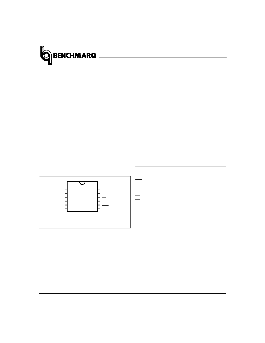
Integrated Backup Unit
bq2502
1
PN250201.eps
12-Pin 600-mil DIP Module
2
3
4
5
6
12
11
10
9
8
7
VCC
CE
CECON1
CECON2
NC
RST
VOUT
NC
A
NC
THS
VSS
Pin Names
V
OUT
Supply output
RST
Reset output
THS
Threshold select input
CE
chip-enable active low input
CE
CON1
,
Conditioned chip-enable outputs
CE
CON2
A
Bank select input
NC
No connect
V
CC
5-volt supply input
V
SS
Ground
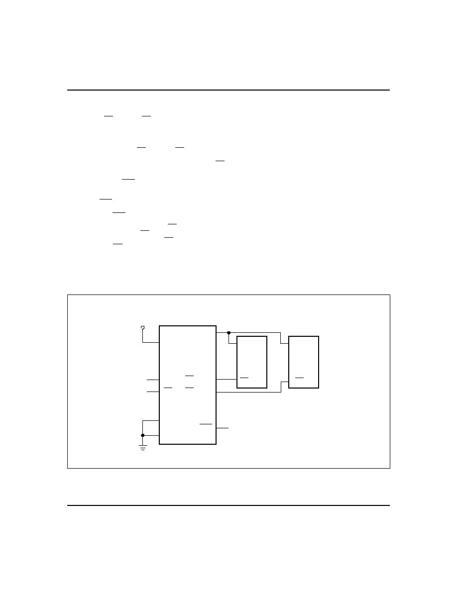
Two banks of CMOS static RAM can be battery-backed
using the V
OUT
and conditioned chip-enable output pins
from the bq2502. As the voltage input V
CC
slews down
during a power failure, the two conditioned chip-enable
outputs, CE
CON1
and CE
CON2
, are forced inactive
independent of the chip-enable input CE.
This activity unconditionally write-protects external SRAM
as V
CC
falls to an out-of-tolerance threshold V
PFD
. V
PFD
is
selected by the threshold-select input pin, THS. If THS is
tied to V
SS
, the power-fail detection occurs at 4.62V typical
for 5% supply operation.
Apr. 1991
Functional Description
Pin Connections
If THS is tied to V
OUT
, power-fail detection occurs at
4.37V typical for 10% supply operation. The THS pin
must be tied to V
SS
or V
OUT
for proper operation.
If a memory access is in process to any of the two exter-
nal banks of SRAM during power-fail detection, that
memory cycle continues to completion before the memory
is write-protected. If the memory cycle is not terminated
within time t
WPT
(150
µ
s maximum), the two chip-enable
outputs are unconditionally driven high, write-protecting
the controlled SRAMs.
As the supply continues to fall past V
PFD
, an internal
switching device forces V
OUT
to the internal backup en-
ergy source. CE
CON1
and CE
CON2
are held high by the
V
OUT
energy source.
During power-up, V
OUT
is switched back to the 5V sup-
ply as V
CC
rises above the backup cell input voltage
sourcing V
OUT
. Outputs CE
CON1
and CE
CON2
are held
inactive for time t
CER
(120ms maximum) after the
power supply has reached V
PFD
, independent of the CE
input, to allow for processor stabilization.
The reset output (RST) goes active within t
R
(150
µ
s
maximum) after V
PFD,
and remains active for a mini-
mum of 40ms (120ms maximum) after power returns
valid. The RST output can be used as the power-on re-
set for a microprocessor. Access to the external RAM
may begin when RST returns inactive.
During power-valid operation, the CE input is passed
through to one of the two CE
CON
outputs with a propa-
gation delay of less than 10ns. The CE input is output on
one of the two CE
CON
output pins depending on the
level of bank select input A, as shown in the Truth Ta-
ble.
Bank select input A is usually tied to a high-order address
pin so that a large nonvolatile memory can be designed
using lower-density memory devices. Nonvolatility and de-
coding are achieved by hardware hookup, as shown in Fig-
ure 1.
The internal lithium cell is capable of supplying 3V on
V
OUT
for an extended period. The cumulative length of
time that the external SRAMs retain data in the ab-
sence of power is a function of the data-retention cur-
rent of the SRAMs used. The initial capacity of the in-
ternal lithium cell is 130mAh. Typically, if the data- re-
tention currents for two external SRAMs are 1
µ
A per
SRAM at room temperature, nonvolatility is calculated
to be for more than 7 years. If only one external SRAM
is used, the data-retention time increases to more than
13 years.
The bq2502 battery life is a function of the time spent in
battery-backed mode and the data-retention current of
the external SRAM. For example, office equipment is
generally powered on for 8 hours and powered off for 16
hours. Under these conditions, a single bq2502 provides
SRAMs drawing 2
µ
A total data-retention current with
more than 10 years of nonvolatility.
2
FG250201.eps
VCC
CE
THS
VSS
VOUT
bq2502
VCC
CE
CMOS
SRAM
5V
CECON2
RST
CECON1
A
VCC
CE
CMOS
SRAM
To Microprocessor
Figure 1. Hardware Hookup (5% Supply Operation)
Apr. 1991
bq2502

As shipped from Benchmarq, the internal lithium cell is
electrically isolated from V
OUT
, CE
CON1
, and CE
CON2
.
Self-discharge in this condition is less than 0.5% per
year at 20∞C.
Note: Following the first application of V
CC
, this isola-
tion is broken, and the backup cell provides power to
V
OUT
, CE
CON1
, and CE
CON2
for the external SRAM.
This isolation can be reestablished by applying a valid
isolation signal to the bq2502. See Figure 2. This signal
requires CE low as V
CC
crosses both V
PFD
and V
SO
dur-
ing a power--down. Between these two points in time,
CE must be brought to (0.48 to 0.52) * V
CC
and held for
at least 700ns. The isolation signal is invalid if CE ex-
ceeds 0.54*V
CC
at any point between V
CC
crossing
V
PFD
and V
SO
.
The battery is connected to V
OUT
immediately on subse-
quent application and removal of V
CC
.
3
TD220201.eps
VCC
CE
VPFD
VSO
0.5 VCC
700ns
Figure 2. Battery Isolation Signal
Truth Table
Input
Output
CE
A
CE
CON1
CE
CON2
H
X
H
H
L
L
L
H
L
H
H
L
Apr. 1991
Caution:
Take care to avoid inadvertent discharge through
V
OUT
, CE
CON1
, and CE
CON2
after battery isolation
has been broken.
bq2502
4
Recommended DC Operating Conditions
(TA = 0 to 70∞C)
Symbol
Parameter
Minimum
Typical
Maximum
Unit
Notes
V
CC
Supply voltage
4.75
5.0
5.5
V
THS = V
SS
4.50
5.0
5.5
V
THS = V
OUT
V
SS
Supply voltage
0
0
0
V
V
IL
Input low voltage
-0.3
-
0.8
V
V
IH
Input high voltage
2.2
-
V
CC
+ 0.3
V
THS
Threshold select
-0.3
-
V
CC
+ 0.3
V
Note:
Typical values indicate operation at T
A
= 25∞C, V
CC
= 5V or V
BAT
.
Absolute Maximum Ratings
Symbol
Parameter
Value
Unit
Conditions
V
CC
DC voltage applied on V
CC
relative to V
SS
-0.3 to +7.0
V
V
T
DC voltage applied on any pin excluding V
CC
relative to V
SS
-0.3 to +7.0
V
V
T
V
CC
+ 0.3
T
OPR
Operating temperature
0 to 70
∞C
T
STG
Storage temperature
-40 to +70
∞C
T
BIAS
Temperature under bias
-10 to +70
∞C
T
SOLDER
Soldering temperature
260
∞C
For 10 seconds
I
OUT
V
OUT
current
200
mA
Note:
Permanent device damage may occur if Absolute Maximum Ratings are exceeded. Functional opera-
tion should be limited to the Recommended DC Operating Conditions detailed in this data sheet. Expo-
sure to conditions beyond the operational limits for extended periods of time may affect device reliability.
Apr. 1991
bq2502
5
DC Electrical Characteristics
(TA = 0 to 70∞C, VCC = 5V
±
10%)
Symbol
Parameter
Minimum
Typical
Maximum
Unit
Conditions/Notes
C
Battery capacity
-
130
-
mAhr
Refer to graphs in Typical
Battery Characteristics
section.
I
LI
Input leakage current
-
-
±
1
µ
A
V
IN
= V
SS
to V
CC
V
OH
Output high voltage
2.4
-
-
V
I
OH
= -2.0mA
V
OHB
V
OH
, backup supply
V
BAT
- 0.3
-
-
V
V
BAT
> V
CC
, I
OH
= -10
µ
A
V
OL
Output low voltage
-
-
0.4
V
I
OL
= 4.0mA
V
BAT
Internal battery voltage
-
2.9
-
V
Refer to graphs in Typical
Battery Characteristics
section.
I
CC
Operating supply current
-
3
6
mA
No load on V
OUT
, CE
CON1
,
CE
CON2
, and RST.
V
PFD
Power-fail detect voltage
4.55
4.62
4.75
V
THS = V
SS
4.30
4.37
4.50
V
THS = V
OUT
V
SO
Supply switch-over voltage
-
2.9
-
V
I
CCDR
Data-retention mode
current from internal battery
-
-
100
nA
No load on V
OUT
, CE
CON1
,
CE
CON2
, and RST.
V
OUT1
V
OUT
voltage
V
CC
- 0.2
-
-
V
V
CC
> V
BAT
, I
OUT
= 100mA
V
CC
- 0.3
-
-
V
V
CC
> V
BAT
, I
OUT
= 160mA
V
OUT2
V
OUT
voltage from internal
battery
VBAT - 0.2
-
-
V
V
CC
< V
BAT
, I
OUT
= 100
µ
A,
from internal battery
I
OUT1
V
OUT
current
-
-
160
mA
V
OUT
V
CC
- 0.3V
Note:
Typical values indicate operation at T
A
= 25∞C, V
CC
= 5V or V
BAT
.
Capacitance
(TA = 25∞C, F = 1MHz, VCC = 5.0V)
Symbol
Parameter
Minimum
Typical
Maximum
Unit
Conditions
C
IN
Input capacitance
-
-
8
pF
Input voltage = 0V
C
OUT
Output capacitance
-
-
10
pF
Output voltage = 0V
Note:
This parameter is sampled and not 100% tested.
Apr. 1991
bq2502