Äîêóìåíòàöèÿ è îïèñàíèÿ www.docs.chipfind.ru
www.ti.com
FEATURES
APPLICATIONS
DESCRIPTION
SDQ
P-
C1
0.1 F
m
+
VSS
CO
BAT
OC
DO
bq26100
SDQ
VSS
NC
PWR
NC
NC
R1
4.7 kW
P+
Protector
bq26100
SLUS696 JUNE 2006
SHA-1/HMAC BASED SECURITY AND AUTHENTICATION IC WITH SDQ INTERFACE
·
Cellular Phones
·
Provides Authentication of Battery Packs
Through SHA-1 Engine Based HMAC
·
PDA and Smart Phones
·
MP3 Players
·
160 Bytes OTP, 16 Bytes EEPROM
·
Digital Cameras
·
Internal Time-Base Eliminates External
·
Internet Appliances
Crystal Oscillator
·
Handheld Devices
·
Low Power Operating Modes:
Active: < 50
µ
A
Sleep: 8
µ
A Typical
·
Single-Wire SDQ Interface
·
Powers Directly From the Communication
Bus
·
6 Lead SON Package
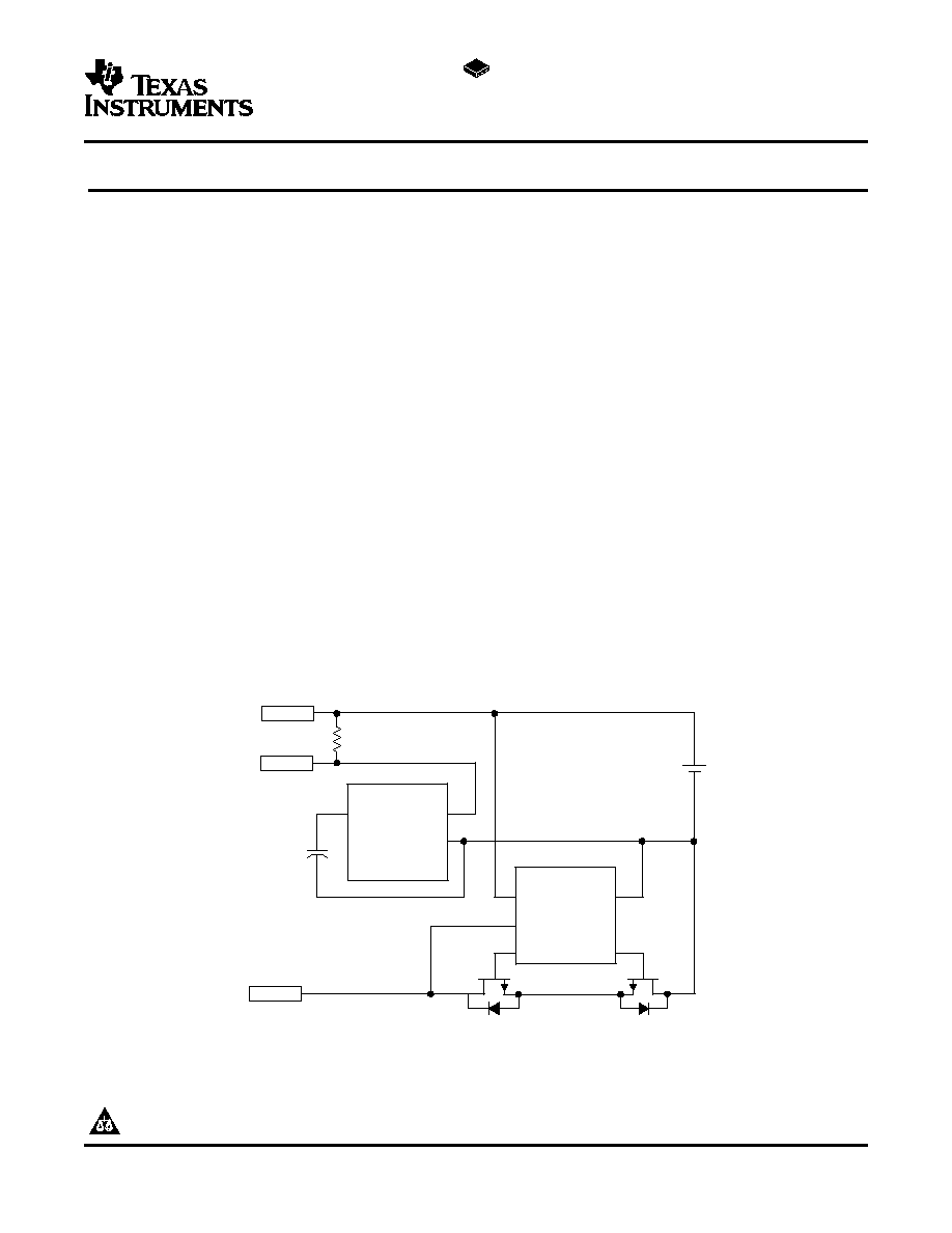
The bq26100 provides a method to authenticate battery packs, ensuring that only packs manufactured by
authorized sub-contractors are used in the end application. The security is achieved using the SHA-1 hash
function inside the widely adopted HMAC construction. A unique 128-bit key is stored in each bq26100 device,
allowing the host to authenticate each pack.
The bq26100 communicates to the system over a simple one-wire bi-directional serial interface. The 5-kbits/s
SDQ bus interface reduces communications overhead in the external microcontroller. The bq26100 also derives
power over the SDQ bus line via an external capacitor.
TYPICAL APPLICATION
Please be aware that an important notice concerning availability, standard warranty, and use in critical applications of Texas
Instruments semiconductor products and disclaimers thereto appears at the end of this data sheet.
PRODUCTION DATA information is current as of publication date.
Copyright © 2006, Texas Instruments Incorporated
Products conform to specifications per the terms of the Texas
Instruments standard warranty. Production processing does not
necessarily include testing of all parameters.

www.ti.com
ABSOLUTE MAXIMUM RATINGS
(1)
RECOMMENDED OPERATING CONDITIONS
ELECTRICAL CHARACTERISTICS
STANDARD SERIAL COMMUNICATION (SDQ) TIMING
bq26100
SLUS696 JUNE 2006
ORDERING INFORMATION
T
A
PACKAGE
PART NUMBER
40
°
C to 85
°
C
6-lead SON
bq26100DRP
VALUE
UNIT
Supply voltage (SDQ all with respect to VSS)
0.3 to 7.7
V
Output current (SDQ)
5
mA
T
A
Operating free-air temperature range
40 to 85
°
C
T
stg
Storage temperature range
65 to 150
°
C
T
J
Junction temperature range
40 to 90
°
C
Lead temperature (Soldering, 10 sec)
300
°
C
(1)
Stresses beyond those listed under absolute maximum ratings may cause permanent damage to the device. These are stress ratings
only, and functional operation of the device at these or any other conditions beyond those indicated under recommended operating
conditions is not implied. Exposure to absolute-maximum-rated conditions for extended periods may affect device reliability.
over operating free-air temperature range (unless otherwise noted)
MIN
MAX
UNIT
V
sdq
Pull-up voltage
2.5
5.0
V
T
J
Operating free-air temperature range
40
85
°
C
all parameters over operating free-air temperature and supply voltage range (unless otherwise noted) (memory programming
and authentication were tested with R1 = 4.7 k
, C1 = 0.1
µ
F over pull-up voltage range)
PARAMETER
TEST CONDITIONS
MIN
TYP
MAX
UNIT
Power up communication delay
Power capacitor charge time
100
ms
I
sleep
Sleep current
8
11
µ
A
I
sdq(Vsdq)
V
sdq
Current
V
sdq
V
sdq(min)
50
µ
A
OTP Memory programming voltage
6.8
7
7.7
V
OTP Memory programming time
100
µ
s/byte
EEPROM Programming current (peak current)
83
µ
A
EEPROM Peak current duration
100
µ
s
EEPROM Programming time
50
ms
SDQ
V
IL
Input low-level voltage
0.63
V
I
OL
Output low sink current
V
OL
= 0.4 V
1
mA
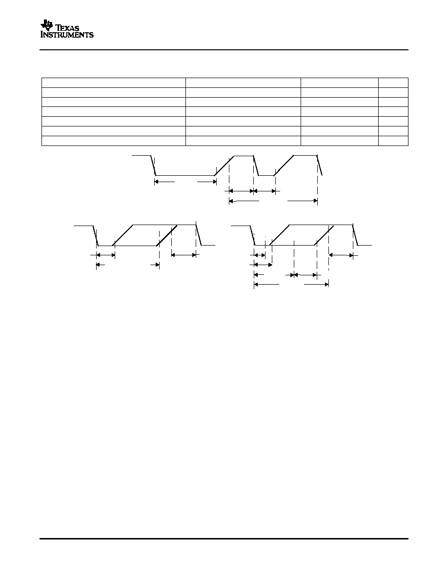
over recommended operating temperature and supply voltage range (unless otherwise noted) (See
Figure 1
)
PARAMETER
TEST CONDITIONS
MIN
TYP
MAX
UNIT
t
RSTL
Reset time low
480
µ
s
t
RSTH
Reset time high
480
µ
s
t
PDL
Presence detect low
60
240
µ
s
t
PDH
Presence detect high
15
60
µ
s
t
REC
Recovery time
1
µ
s
t
SLOT
Host bit window
60
120
µ
s
t
LOW1
Host sends 1
1
13
µ
s
2
Submit Documentation Feedback
www.ti.com
t
PDH
t
PDL
t
RSTL
t
RSTH
(c) bq26100 Transmitted Bit Timing
(a) Reset and Presence Timing
(b) Host Transmitted Bit Timing
t
LOW1
t
LOW0
SLOT
& t
t
SU
t
REC
t
RELEASE
t
REC
t
SLOT
t
RDV
t
LOWR
bq26100
SLUS696 JUNE 2006
STANDARD SERIAL COMMUNICATION (SDQ) TIMING (continued)
over recommended operating temperature and supply voltage range (unless otherwise noted) (See
Figure 1
)
PARAMETER
TEST CONDITIONS
MIN
TYP
MAX
UNIT
t
LOW0
Host sends 0
60
120
µ
s
t
LOWR
Host read bit start
1
13
µ
s
t
SLOT
bq26100 bit window
60
120
µ
s
t
SU
bq26100 data setup
1
µ
s
t
RDV
bq26100 data valid
exactly 15
µ
s
t
RELEASE
bq26100 data release
0
15
45
µ
s
Figure 1. SDQ Timing Diagrams
The SDQ protocol requires a CRC calculation as part of the communication flow. The CRC, based on a
polynomial of x
8
+x
5
+x
4
+1, is computed to determine data integrity and its use varies in the protocol. The Memory
Function flows show what data is shifted through the CRC and when the value is transmitted from the slave.
Each data byte used in the CRC calculation is pushed through the CRC shift register from LSB to MSB. The
byte wide CRC computation is:
for (i = 0; i < 8; i++)
{
if (crc[0] ^ input[i])
crc = (crc >> 1) ^ 0x8C;
else
crc = crc >> 1;
}
Where did the magic number 0x8C come from? CRC polynomials are defined such that the highest order simply
shows the number of bits, so x
8
+x
5
+x
4
+1 defines an 8-bit value with a binary value of 00110001 (bits 0, 4, and 5
are 1 and all others are 0). Since the SDQ CRC is computed by shifting in the LSB, the polynomial must be
used in reverse bit order binary 10001100 or hexadecimal 0x8C.
The CRC value is reset to 0 prior to the first byte being shifted through. The CRC is also reset when the CRC is
shifted out as part of the SDQ protocol.
3
Submit Documentation Feedback
www.ti.com
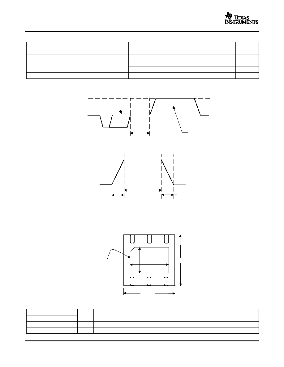
OTP PROGRAMMING SPECIFICATIONS
Last bit before
programming pulse
t
pon
GND
V
pull-up
V
prog
Programming
Pulse
t
rise
t
fall
t
prog
PIN ASSIGNMENT
2.3 mm
4
6
5
3
1
2
Exposed
Thermal Pad
3 mm
3 mm
1.6 mm
bq26100
SLUS696 JUNE 2006
PARAMETER
TEST CONDITIONS
MIN
TYP
MAX
UNIT
t
pon
Program setup time
2
µ
s
t
rise
Pulse rise time
1
10
µ
s
t
prog
Pulse high time
Single byte programming
300
µ
s
Key programming
3
µ
s
t
fall
Pulse fall time
1
10
µ
s
Figure 2. bq26100 Communication to OTP Programming Pulse Diagram
Figure 3. OTP Programming Pulse Detail
TERMINAL FUNCTIONS
TERMINAL
I/O
DESCRIPTION
NAME
NO.
NC
2, 3, 4
No connect
PWR
1
I/O
Power capacitor connection
4
Submit Documentation Feedback
www.ti.com
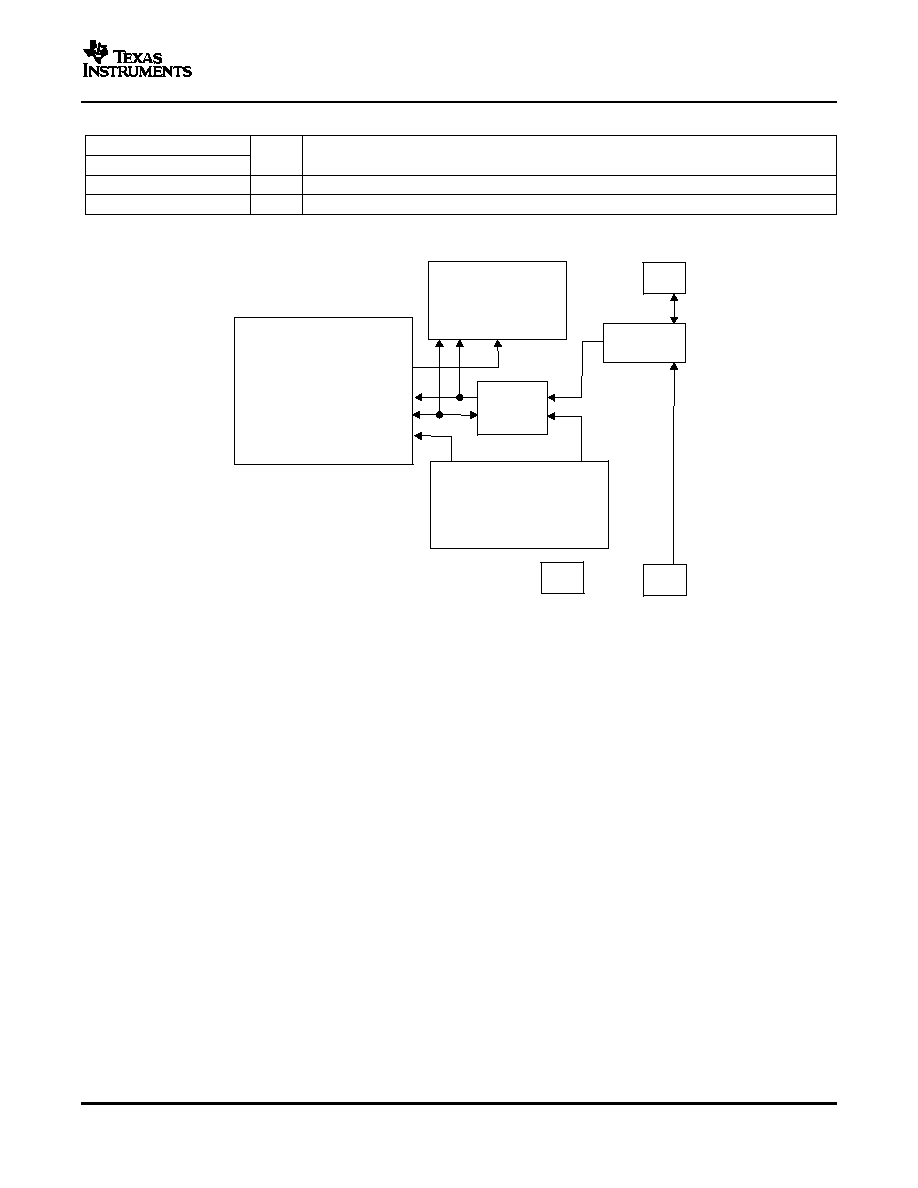
EEPROM
- Charge Pump
DTOP
- SHA-1/HMAC
- SDQ
- Ctrl and Status Registers
Power
Retification
ATOP
- Oscillator
- LDO
- POR
- OTP Power Comparator
VSS
OTP
PWR
SDQ
FUNCTIONAL DESCRIPTION
bq26100
SLUS696 JUNE 2006
TERMINAL FUNCTIONS (continued)
TERMINAL
I/O
DESCRIPTION
NAME
NO.
SDQ
6
I/O
Single wire SDQ interface to host
VSS
5
I
Ground
FUNCTIONAL BLOCK DIAGRAM
The bq26100 provides the same basic functionality as the bq2022 with added battery pack/accessory
authentication functions. In addition to four 32-byte pages of general use One Time Programmable (OTP)
non-volatile memory available on the bq2022, the bq26100 adds a fifth 32-byte page of OTP and a 16-byte page
of EEPROM to be used at the host system designer's discretion. An external high voltage is required for
programming the OTP, but not necessary for programming the EEPROM.
A modified form of the SHA-1/HMAC provides the authentication function of the bq26100. Both the host and the
bq26100 share two 64-bit keys used in the authentication calculation. To authenticate a battery pack, the host
writes a random 20-byte message to the bq26100 and sets the AUTH bit in the CTRL register. The bq26100
calculates the HMAC digest in less than 500
µ
s, replacing the random message sent by the host with the HMAC
result. To complete the authentication process, the host computes the HMAC function with the same 20-byte
random message originally written to the bq26100. The result is compared to the HMAC result computed by the
bq26100. If the values match, the pack is authenticated.
The key is separated into two 64-bit spaces, allowing multiple parties to program separate portions of the key
and providing an added level of security. Programming a key utilizes the SHA-1 algorithm to provide a mix from
the values used to program the device to the actual key stored on the device. When put into key programming
mode, the device combines the 160-bit message space with a pad as required to get the minimum 512-bit
SHA-1 block, and run through the SHA-1 engine once. The 160-bit output is truncated to the lower 64 bits,
scrambled internally, and then written to the appropriate non-volatile memory key space. The key can only be
read and descrambled by the authentication engine, not by the communication engine, of the bq26100.
5
Submit Documentation Feedback
Document Outline