High-Performance Battery Coulomb Counter for Cellular Phone Applications
bq26200
SLUS509 DECEMBER 2001
HIGH PERFORMANCE BATTERY MONITOR
WITH COLOUMB COUNTER AND FLASH MEMORY
1
www.ti.com
FEATURES
D
Multifunction Monitoring Device Designed to
Work With an Intelligent Host Controller
Provides State of Charge Information for
Rechargeable Batteries
Enhances Charge Termination
D
High Accuracy Coulometric Charge and
Discharge Current Integration With Automatic
Offset Compensation
D
Differential Current Sense
D
32 Bytes of General-Purpose RAM
D
96 Bytes of Flash (Including 32 Bytes of
Shadow Flash)
D
8 Bytes of ID ROM
D
Internal Temperature Sensor Eliminates Need
for External Thermistor
D
Multifunction Digital Output Port
D
High-Accuracy Internal Timebase Eliminates
External Crystal Oscillator
D
Low Power Consumption
Operating : <95
µ
A
Sleep: <2
µ
A
D
Single-Wire HDQ Serial Interface
D
8-Lead TSSOP Package
DESCRIPTION
The bq26200 is an advanced battery monitoring IC
designed to accurately measure the charge and
discharge currents in rechargeable battery packs.
Intended for pack integration, the bq26200 contains all
the necessary functions to form the basis of a
comprehensive battery capacity management system
in portable applications such as cellular phones, PDA's,
or other portable products.
The bq26200 works with the host controller in the
portable system to implement the battery management
system. The host controller is responsible for
interpreting the bq26200 data and communicating
meaningful battery data to the end-user or power
management system.
The bq26200 provides 64 bytes of general-purpose
flash memory, 8 bytes of ID ROM and 32 bytes of flash
backed RAM for data storage. The non-volatile memory
can maintain formatted battery monitor information,
identification codes, warranty information, or other
critical battery parameters during periods when the
battery is temporarily shorted or deeply discharged.
1
2
3
4
8
7
6
5
REG
VCC
VSS
HDQ
STAT
SRP
SRN
OSC
PW PACKAGE
(TOP VIEW)
AVAILABLE OPTIONS
T
MARKING
PACKAGE
T
A
MARKING
TSSOP (PW)
20
°
C to 70
°
C
bq262
bq26200PW
PRODUCTION DATA information is current as of publication date.
Products conform to specifications per the terms of Texas Instruments
standard warranty. Production processing does not necessarily include
testing of all parameters.
Copyright
2001, Texas Instruments Incorporated
Please be aware that an important notice concerning availability, standard warranty, and use in critical applications of
Texas Instruments semiconductor products and disclaimers thereto appears at the end of this data sheet.
bq26200
SLUS509 DECEMBER 2001
2
www.ti.com
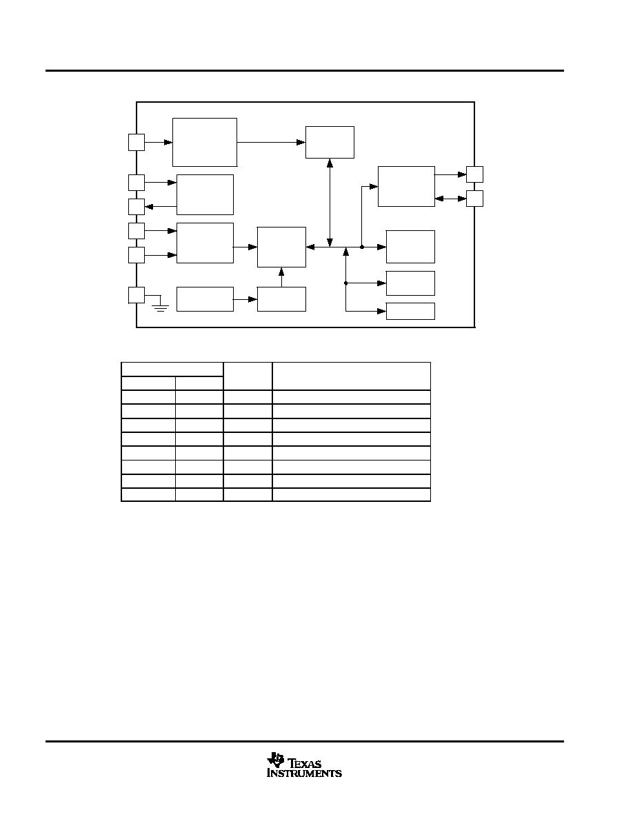
functional block diagram
UDG01132
2
1
7
6
3
Bandgap,
Reference
and Bias
Temperature
Compensated
Precision
Oscillator
Timer
Auto
Calibrating
VFC
RAM
ADC
Temperature
Sensor
System I/O
and Control
User
Registers
Flash
ID
8
4
5
OSC
VCC
REG
SRP
SRN
VSS
STAT
HDQ
terminal functions
TERMINAL
I/O
DESCRIPTION
NAME
No.
I/O
DESCRIPTION
HDQ
4
I/O
Single-wire HDQ interface
OSC
5
O
Time base adjust for the oscillator
REG
1
O
Regulator output
SRN
6
I
Current sense input 2
SRP
7
I
Current sense input 1
STAT
8
O
Open-drain status output
VCC
2
I
Supply voltage
VSS
3
Ground
bq26200
SLUS509 DECEMBER 2001
3
www.ti.com
absolute maximum ratings over operating freeair temperature range (unless otherwise noted)
Supply voltage (V
CC
with respect to GND)
0.3 to +7.0 V
. . . . . . . . . . . . . . . . . . . . . . . . . . . . . . . . . . . . . . . . . . .
Input voltage, SRP and SRN (all with respect to GND)
0.3 V to V
CC
+0.3 V
. . . . . . . . . . . . . . . . . . . . . . . . . . . .
Output current (STAT)
5 mA
. . . . . . . . . . . . . . . . . . . . . . . . . . . . . . . . . . . . . . . . . . . . . . . . . . . . . . . . . . . . . . . . . . . . . .
Output current (REG)
400 nA
. . . . . . . . . . . . . . . . . . . . . . . . . . . . . . . . . . . . . . . . . . . . . . . . . . . . . . . . . . . . . . . . . . . . .
Output current (HDQ)
5 mA
. . . . . . . . . . . . . . . . . . . . . . . . . . . . . . . . . . . . . . . . . . . . . . . . . . . . . . . . . . . . . . . . . . . . . . .
Operating free-air temperature range, T
A
20
_
C to 70
_
C
. . . . . . . . . . . . . . . . . . . . . . . . . . . . . . . . . . . . . . . . . . . .
Storage temperature range, T
stg
55
_
C to 150
_
C
. . . . . . . . . . . . . . . . . . . . . . . . . . . . . . . . . . . . . . . . . . . . . . . . .
Lead temperature (soldering, 10 s)
300
_
C
. . . . . . . . . . . . . . . . . . . . . . . . . . . . . . . . . . . . . . . . . . . . . . . . . . . . . . . . . .
Stresses beyond those listed under absolute maximum ratings may cause permanent damage to the device. These are stress ratings only, and
operation of the device at these or any other conditions beyond those indicated under recommended operating conditions is not implied. Exposure
to absolute-maximum-rated conditions for extended periods may affect device reliability.
recommended operating conditions
PARAMETER
TEST CONDITIONS
MIN
MAX
UNIT
VCC
Supply voltage
2.8
5.5
V
TA
Operating ambient temperature
20
70
_
C
dc electrical characteristics over recommended operating temperature and supply voltage (unless
otherwise noted)
PARAMETER
TEST CONDITIONS
MIN
TYP
MAX
UNIT
I
Supply current
VCC = 5.5 V, flash programming not active
88
120
µ
A
ICC(OP)
Supply current
VCC = 4.3 V, flash programming not active
78
95
µ
A
I(SLEEP)
Sleep current
2.8 V
VCC
4.3 V,
flash programming not active
1
2
µ
A
ICC(PROG) Flash programming supply current
VCC = 5.5 V
22
25
mA
ICC(ERASE) Flash erase supply current
VCC = 5.5 V
14
25
mA
VOL
Digital output low HDQ
IOL = 1 mA
0.4
V
IOL
Digital output low sink current
350
µ
A
VIL
Digital input low HDQ pin
0.7
V
V
Digital inp t high HDQ pin
VCC < 4.2 V
1.7
V
VIH
Digital input high HDQ pin
VCC > 4.2 V
1.9
V
RSR
SR input impedance
0.2 V < (V(SRP) V(SRN)
)
< VCC
10
M
ac electrical characteristics over recommended operating temperature and supply voltage (unless
otherwise noted)
PARAMETER
TEST CONDITIONS
MIN
TYP
MAX
UNIT
td(OR)
Power on reset delay
See Note 1
500
ms
NOTES:
1. Delay time after VCC is at least 2.8 V before HDQ communication is attempted.
REG amplifier characteristics over recommended operating temperature and supply voltage
(unless otherwise noted)
PARAMETER
TEST CONDITIONS
MIN
TYP
MAX
UNIT
V(TH)
Regulator threshold
4.5
4.75
5.0
V
bq26200
SLUS509 DECEMBER 2001
4
www.ti.com
timer
PARAMETER
TEST CONDITIONS
MIN
TYP
MAX
UNIT
R(OSC)
Oscillator current coefficient
10
ppm/
E(TMR)
Timer accuracy error
R(OSC) = 100 k (
±
0.1%),
See Note 1
3%
3%
NOTES:
1. Timer accuracy is linearly proportional to the tolerance of R(OSC).
NOTES:
2. Variation of oscillator frequency due to change in R(OSC).
temperature register
PARAMETER
TEST CONDITIONS
MIN
TYP
MAX
UNIT
T(RES)
Reported temperature resolution
1
_
k
E(T)
Reported temperature accuracy
VCC = 3.6 V
3
3
_
K
Reported temperature drift
2
_
kV
VFC
PARAMETER
TEST CONDITIONS
MIN
TYP
MAX
UNIT
VI(SR)
Input voltage: VSRP VSRN
100
100
mV
G(VFC)
Charge/discharge gain
TA = 25
_
C, VCC = 3.6
89.2
92.2
95.2
Hz/V
G(VCC)
Supply voltage gain coefficient
100 mV < (V(SRP) V(SRN)
)
< 100 mV
0.45
0.86
%/V
Slope ( 20
_
C
TA
70
_
C)
0.03
0.02
%/
_
C
G
Temperature gain coefficient
Total deviation ( 20
_
C
TA
70
_
C)
0.15%
0.56%
G(TCO)
Temperature gain coefficient
Slope ( 0
_
C
TA
50
_
C)
0.03
0.03
%/
_
C
Total deviation ( 0
_
C
TA
50
_
C)
0.06%
0.51%
INL
Integrated non-linearity
100 mV < (V(SRP) V(SRN)
)
< 100 mV
0.2%
0.5%
V(COS)
Auto compensated offset
2.8 V
Vcc
4.3 V, R(OSC) = 100 K (
±
1%)
17.7
12.5
µ
V
flash memory
PARAMETER
TEST CONDITIONS
MIN
TYP
MAX
UNIT
Data retention
5
Years
Flash programming write-cycles
10,000
Cycles
t(BYTEPROG) Byte programming time
90
µ
s
t(BLCKPROG) RAM-to-flash block programming
time
60
µ
s +30
µ
s/byte
1020
µ
s
t(BLKERASE) Block-erase time
60
µ
s +30
µ
s/byte
1020
µ
s
bq26200
SLUS509 DECEMBER 2001
5
www.ti.com
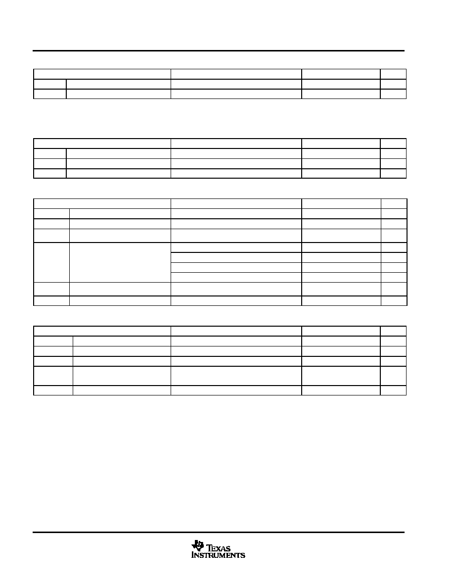
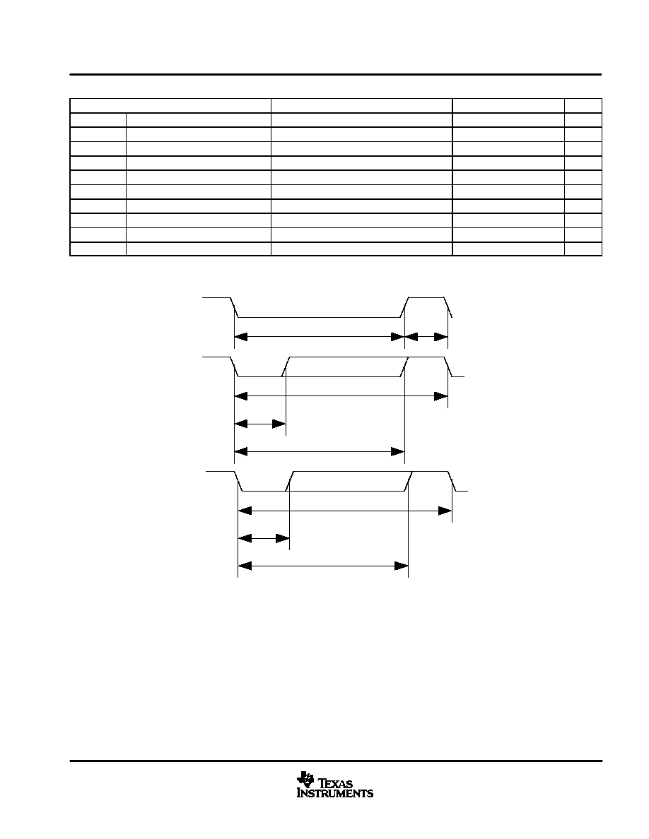
standard serial communication (HDQ) timing, See Figures 1 and 2.
PARAMETER
TEST CONDITIONS
MIN
TYP
MAX
UNIT
t(B)
Break timing
190
µ
s
t(BR)
Break recovery time
40
µ
s
t(CYCH)
Host bit window
190
µ
s
t(HW1)
Host sends 1
32
50
µ
s
t(HW0)
Host sends 0
100
145
µ
s
t(RSPS)
bq26200 to host response
190
320
µ
s
t(CYCD)
bq26200 bit window
190
250
µ
s
t(startdetect) See Note 1
5
ns
t(DW1)
Sends 1
bq26200
32
50
µ
s
t(DW0)
Sends 0
bq26200
80
145
µ
s
NOTES:
1. The HDQ engine of the bq26220 inteprets a 5 ns or longer glitch on HDQ as a bit start. A sufficient number of glitches 5 ns or longer
could result in incorrect data being written to the device. The HDQ line should be properly deglitched to ensure that this does not
occur.
t
(CYCH)
t
(HW1)
t
(HW0)
t
(CYCD)
t
(DW1)
t
(DW0)
t
(B)
t
(BR)
UDG01149
Figure 1. HDQ Timing Diagram