bq26501
SLUS586B - OCTOBER 2003 - REVISED MARCH 2004
SINGLE CELL LI ION AND LI POL BATTERY GAS GAUGE IC
FOR HANDHELD APPLICATIONS (bqJUNIORt FAMILY)
1
www.ti.com
FEATURES
D
Reports Accurate State-of-Charge in Li-Ion
and Li-Pol Cells, No System Processor
Calculations Needed
D
Communicates Directly With the Integrated
HDQ Engine in TI OMAP
t
Processors
D
Reports Cell Temperature and Voltage
D
High-Accuracy Coulometric Charge and
Discharge Current Integration with
Automatic Offset Cancellation
D
Requires No Offset Calibration
D
Programmable Input/Output Port
D
Internal Time-Base Eliminates External
Crystal Oscillator
D
Four Automatic Low-Power Operating Modes
- Active: < 100
�
A
- Sleep: < 2.5
�
A
- Ship: < 1.7
�
A
- Hibernate: < 1.5
�
A
D
Small 8-Pin TSSOP Package
APPLICATIONS
D
PDAs
D
Smart Phones
D
MP3 Players
D
Digital Cameras
D
Internet Appliances
D
Handheld Devices
DESCRIPTION
The bq26501, the first in the bqJUNIOR
t
family
of advanced gas gauge device for handhald
applications, is a highly accurate standalone
single-cell Li-Ion and Li-Pol battery capacity
monitoring and reporting device targeted at space
limited portable applications. The device monitors
a voltage drop across a small current sense
resistor connected in series with the battery to
determine charge and discharge activity of the
battery. Compensations for battery temperature,
self-discharge, and rate of discharge are applied
to the charge counter to provide available capacity
across a wide range of operating conditions.
Battery capacity is automatically recalibrated, or
learned, in the course of a discharge cycle from full
to empty. Internal registers include available
capacity, cell temperature and voltage,
state-of-charge, and status and control registers.
The bq26501 can operate directly from single-cell
Li-Ion and Li-Pol batteries and communicates to
the system over a simple one-wire bi-directional
serial interface. The 5-kbits/s HDQ bus interface
reduces communication overhead in the external
microcontroller.
PRODUCTION DATA information is current as of publication date.
Products conform to specifications per the terms of Texas Instruments
standard warranty. Production processing does not necessarily include
testing of all parameters.
Copyright
2003-2004, Texas Instruments Incorporated
Please be aware that an important notice concerning availability, standard warranty, and use in critical applications of
Texas Instruments semiconductor products and disclaimers thereto appears at the end of this data sheet.
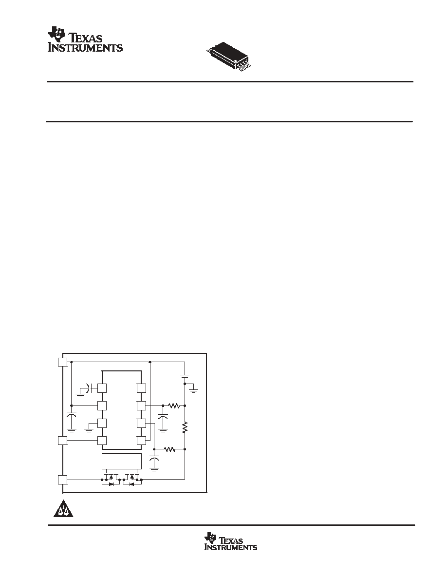
UDG-03038
SIMPLIFIED APPLICATION
1
2
3
4
8
7
6
5
GPIO
SRP
SRN
BAT
RBI
VCC
VSS
HDQ
bq26501
Protection
Controller
+
HDQ
PACK-
PACK+
Battery Pack
Li-Ion
or
Li-Pol
bq26501
SLUS586B - OCTOBER 2003 - REVISED MARCH 2004
2
www.ti.com
ABSOLUTE MAXIMUM RATINGS
over operating free-air temperature range unless otherwise noted(1)
bq26501
UNIT
Supply voltage range, VCC (all with respect to VSS)
-0.3 to 7.0
Input voltage range at SRP, SRN, RBI, and BAT (all with respect to VSS)
-0.3 to VCC + 0.3 V
V
Input voltage
HDQ, GPIO (with respect to VSS)
-0.3 to 7.0
V
Input voltage
GPIO (with respect to VSS) during EEPROM programming only
-0.3 to 22.0
Output sink current at GPIO, HDQ
5
mA
Operating free-air temperature range, TA
-20 to 70
Storage temperature range, Tstg
65
�
C to 150
�
C
�
C
Junction temperature range, TJ
-40
�
C to 125
�
C
�
C
Lead temperature 1,6 mm (1/16 inch) from case for 10 seconds
300
(1) Stresses beyond those listed under "absolute maximum ratings" may cause permanent damage to the device. These are stress ratings only,
and functional operation of the device at these or any other conditions beyond those indicated under "recommended operating conditions" is
not implied. Exposure to Absolute Maximum Rated conditions for extended periods may affect device reliability
RECOMMENDED OPERATING CONDITIONS
MIN
NOM
MAX
UNIT
Supply voltage, VCC
2.6
4.5
V
Operating free-air temperature, TJ
-20
70
�
C
Input voltage range at SRP and SRN, (with respect to VSS)
-100
100
mV
ELECTRICAL CHARACTERISTICS
TJ = -20
�
C to 70
�
C, TJ = TA, 2.6 V
VCC
4.5 V (unless otherwise noted)
PARAMETER
TEST CONDITIONS
MIN
TYP
MAX
UNIT
INPUT CURRENTS
ICC(ACT) Active current
VCC > VCC(min)
60
90
ICC(SLP) Sleep current
1.2
2.5
A
ICC(SHP) Ship current
0.9
1.7
�
A
ICC(POR) Hibernate current
0 V < VCC < V(POR)
0.6
1.5
RBI current
RBI pin only,
VCC < V(POR)
20
nA
V(POR)
POR threshold
2.05
2.55
V
POR threshold hysteresis
100
mV
Input impedance on BAT pin
10
M
Input impedance on SRP, SRN pins
10
M
VOLTAGE MEASUREMENT
Measurement range
VCC = VI(BAT)
2.6
4.5
V
Reported voltage resolution
1
mV
Reported accuracy
-20
20
mV
Voltage update time
2
s
TEMPERATURE MEASUREMENT
Reported temperature resolution
0.25
�
K
Reported temperature accuracy
-3
3
�
K
Temperature update time
2
s

bq26501
SLUS586B - OCTOBER 2003 - REVISED MARCH 2004
3
www.ti.com
ELECTRICAL CHARACTERISTICS(continued)
TJ = -20
�
C to 70
�
C, TJ = TA, 2.6 V
VCC
4.5 V (unless otherwise noted)
PARAMETER
TEST CONDITIONS
MIN
TYP
MAX
UNIT
CAPACITY MEASUREMENT
Voltage-to-frequency converter offset
15
�
V
Voltage-to-frequency converter gain
3
�
VH
Voltage-to-frequency converter gain
variabilty(3)
0
�
C
TA
50
�
C
2%
Voltage-to-frequency input
(VSRP - VSRN)
-100
100
mV
EEPROM PROGRAMMING (VCC
3.0 V, 20
�
C
TA
35
�
C)(1)
tRISE
Programming voltage rise time
1
tPROG
Programming voltage high time
VPROG = 21 V
20
100
ms
tFALL
Programming voltage fall time
1
ms
VPROG
Programming voltage
Applied to GPIO pin
20
22
V
IPROG
EEPROM programming current
Current into GPIO pin
3
mA
IO PORT (GPIO) AND SERIAL INTERFACE (HDQ)
VIH
High-level input voltage
1.9
VIL
Low-level input voltage
0.7
V
VOL
GPIO low-level output voltage
IOL = 0.3 mA
0.4
V
VOL
HDQ low-level output voltage
IOL = 2 mA
0.4
IHDQPD
HDQ internal pull-down current
4.5
�
A
STANDARD SERIAL COMMUNICATION (HDQ) TIMING(2)
t(B)
Break timing
190
t(BR)
Break recovery time
40
t(CYCH)
Host bit window timing
190
t(HW1)
Host sends 1 time
0.5
50
t(HW0)
Host sends 0 time
86
145
�
s
t(RSPS)
bq26501 to host response time
190
320
�
s
t(CYCD)
bq26501 bit window timing
190
260
t(DW1)
bq26501 sends 1 time
32
50
t(DW0)
bq26501 sends 0 time
80
145
(1) Maximum number of programming cycles on the EEPROM is 10 and data retention time is 10 years at TA=85
�
C
(2) See Figure 1.
(3) Not a production tested parameter.
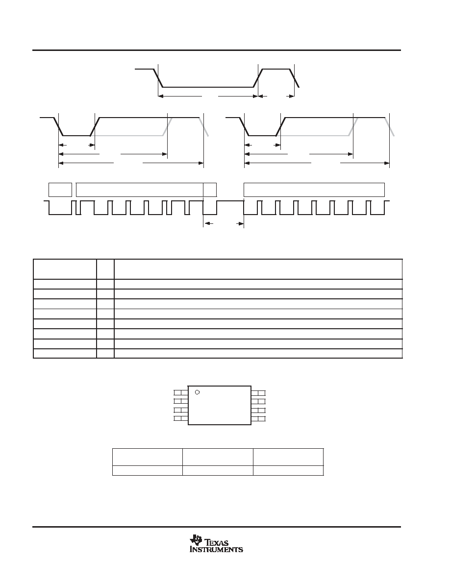
The following timing diagrams describe break and break recovery timing (a), host transmitted bit timing (b),
bq26501 transmitted bit timing (c), and bq26501 to host response timing (d).
bq26501
SLUS586B - OCTOBER 2003 - REVISED MARCH 2004
4
www.ti.com
UDG-03039
(a)
(b)
(c)
(d)
Break
7-Bit Address
R/W
8-Bit Data
t(B)
t(BR)
1-bit
t(HW1)
t(DW1)
t(HW0)
t(DW0)
t(CYCH)
t(CYCD)
t(RSPS)
Figure 1. HDQ Bit Timing Diagrams
PIN ASSIGNMENTS
TERMINAL
I/O
DESCRIPTION
NAME
NO.
I/O
DESCRIPTION
BAT
5
I
Battery voltage sense input
GPIO
8
I/O
General-purpose input/output port
HDQ
4
I/O
Single-wire HDQ serial interface
RBI
1
I
Register back-up input
SRN
6
I
Current sense input (negative)
SRP
7
I
Current sense input (positive)
VCC
2
I
VCC supply input
VSS
3
I
Ground input
1
2
3
4
8
7
6
5
RBI
VCC
VSS
HDQ
GPIO
SRP
SRN
BAT
PW PACKAGE
(TOP VIEW)
AVAILABLE OPTIONS
TA
PACKAGED
DEVICES(1)
MARKINGS
-20
�
C to 70
�
C
bq26501PW
26501
(1) The PW package is available taped and reeled. Add R suffix to device type (e.g. bq26501PWR) to
order quantities of 2,000 devices per reel.
bq26501
SLUS586B - OCTOBER 2003 - REVISED MARCH 2004
5
www.ti.com
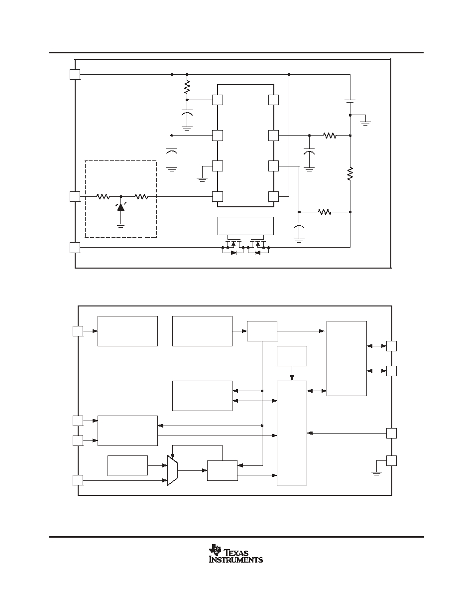
Autocalibration and
Autocompensating
VFC
UDG-03041
1
2
3
4
8
7
6
5
GPIO
SRP
SRN
BAT
RBI
VCC
VSS
HDQ
bq26501
+
HDQ
PACK-
PACK+
Battery Pack
ESD Protection
R4
R3
Protection
Controller
C4
0.1
�
F
C3
0.1
�
F
C2
0.1
�
F
R2
100 k
R1
100 k
C1
0.1
�
F
RS
0.02
Li-Ion
or
Li-Pol
R5
1 M
100
100
D1
5.6 V
Figure 2. Typical Application Circuit
Temperature
Compensated
Precision Oscillator
Clock
Generator
EEPROM
RAM
SCPU
System I/O
and Control
Temperature
Sensor
ADC
2
VCC
7
SRP
6
SRN
5
BAT
4
HDQ
8
GPIO
1
RBI
3
VSS
Autocalibrating and
Autocompensating
VFC
UDG-03040
Bandgap
Reference and
Bias
Figure 3. Functional Block Diagram