bq29311
SLUS487D - DECEMBER 2001 - REVISED NOVEMBER 2003
THREE AND FOUR CELL LITHIUM ION OR
LITHIUM POLYMER BATTERY PROTECTION IC
FEATURES
D
3- or 4-Cell Series Protection Control
D
Autonomous Overcurrent and Short Circuit
Protection
D
Provides Individual Cell Voltages to Battery
Management Host
D
Integrated Cell Balancing Control
D
I
2
C Compatible User Interface Allows Access
to Battery Information
D
User Control to Initiate Protection
D
Integrated 3.3-V 25-mA LDO
D
Programmable Shutdown and Brownout
Control
D
Provides Drive for Three External FETs
D
Low Supply Current of 140
�
A Typical
D
Programmable Threshold and Delay for
Short-Circuit Current Protection
D
Provides Drive for Three External FETs
D
Can Directly Interface With bq2083/5 for
Complete Battery Management Solution
APPLICATIONS
D
Notebook Computer Battery Packs
D
Test Equipment
DESCRIPTION
The bq29311 is a three- or four-cell lithium-ion battery
pack protection analog front end (AFE) IC that
incorporates a 3.3-V 25-mA low-dropout regulator
(LDO) and an I
2
C compatible interface to extract battery
parameters such as cell voltages and control output
status. Other parameters, such as overcurrent
protection threshold and delay, can also be
programmed into the bq29311 to increase the flexibility
of the battery management system.
The bq29311 provides safety protection in overcurrent,
short circuit, overvoltage, and undervoltage conditions
via control from the battery management host. In
overcurrent and short-circuit conditions the bq29311
can directly activate the FET drive as a secondary
protection level. The communications interface allows
the host to control and observe the current status of the
protection, to set overcurrent and overload levels, to set
the overcurrent and overload blanking delay time,
short-circuit threshold levels, and short-circuit blanking
delay time, and to program for the VREG shutdown
voltage and brownout-detection thresholds.
Each cell is balanced by a discharge path, which is
enabled by the internal control registers accessible
through the I
2
C compatible interface. The maximum
current is set by an external series resistor with an
absolute maximum value of 10 mA discharge current
per cell.
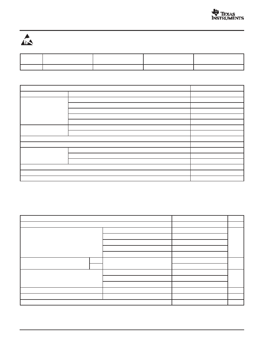
1
2
3
4
5
6
7
8
9
10
11
12
24
23
22
21
20
19
18
17
16
15
14
13
VCC
VBAT
VC1
VC2
VC3
VC4
VC5
SR1
SR2
CNTL
GND
VCELL
VPACK
DSG
PCHG
CHG
LEDOUT
VREG
TOUT
XALERT
CLKIN
SDATA
SCLK
GND
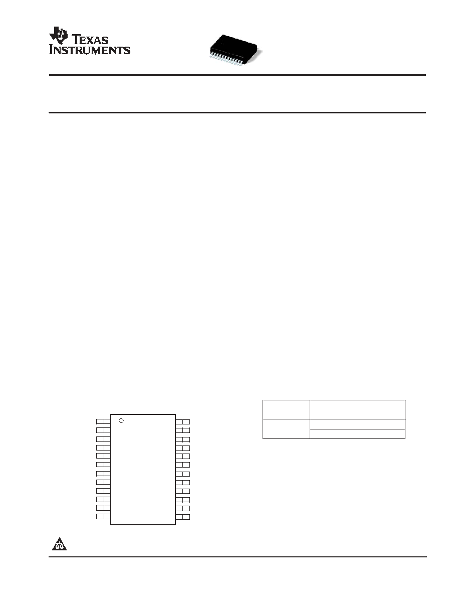
PW PACKAGE
(TOP VIEW)
ORDERING INFORMATION
TA
-25
�
C to 85
�
C
PACKAGED TSSOP
(PW)
bq29311PW
bq29311PWR(1)
PIN ASSIGNMENTS
(1) R suffix indicates tape and reel.
PRODUCTION DATA information is current as of publication date. Products
conform to specifications per the terms of Texas Instruments standard warranty.
Production processing does not necessarily include testing of all parameters.
Please be aware that an important notice concerning availability, standard warranty, and use in critical applications of Texas Instruments
semiconductor products and disclaimers thereto appears at the end of this data sheet.
www.ti.com
Copyright
2001 - 2003, Texas Instruments Incorporated
bq29311
SLUS487D - DECEMBER 2001 - REVISED NOVEMBER 2003
www.ti.com
2
These devices have limited built-in ESD protection. The leads should be shorted together or the device placed in conductive foam during
storage or handling to prevent electrostatic damage to the MOS gates.
PACKAGE DISSIPATION RATINGS
PACKAGE
TA
25
�
C
POWER RATING
DERATING FACTOR
ABOVE TA = 25
�
C
TA = 70
�
C
POWER RATING
TA = 85
�
C
POWER RATING
PW
874 mW
6.99 W/
�
C
559 mW
454 mW
ABSOLUTE MAXIMUM RATINGS
over operating free-air temperature range unless otherwise noted(1)
bq29311
Supply voltage range(2)
VCC, VPACK
-0.3 V to 34 V
VC1, VC2, VC3, VC4, VBAT
-0.3 V to 34 V
VC5, SR1, SR2
-1 V to 1 V
Input voltage range
VC1 to VC2, VC2 to VC3, VC3 to VC4, VC4 to VC5
-0.3 V to 8.5 V
Input voltage range
CLK-IN, SCLK, SDATA
-0.3 V to 7 V
CNTL
-0.3 V to 34 V
Output voltage range
DSG, CHG, PCHG
-0.3 V to VCC
Output voltage range
LEDOUT, TOUT, SCLK, SDATA, VCELL, XALERT
-0.3 V to 7 V
Current for cell balancing
10 mA
Continuous total power dissipation
See Dissipation Rating Table
(3)
HBM
1.5 kV
ESD rating(3)
CDM
250 V
ESD rating(3)
MM
50 V
Operating free-air temperature range, TA
-25
�
C to 85
�
C
Storage temperature range, Tstg
-65
�
C to 150
�
C
Lead temperature (soldering, 10 s)
260
�
C
(1) Stresses beyond those listed under "absolute maximum ratings" may cause permanent damage to the device. These are stress ratings only, and
functional operation of the device at these or any other conditions beyond those indicated under "recommended operating conditions" is not
implied. Exposure to absolute-maximum-rated conditions for extended periods may affect device reliability.
(2) All voltages are with respect to ground of this device except VCn-VC(n+1), where n = 1, 2, 3, 4 cell voltage.
(3) Design considerations should be made with respect to excessive ESD.
RECOMMENDED OPERATING CONDITIONS
MIN
NOM
MAX
UNIT
Supply voltage (VCC or VPACK)
25
V
VBAT
0
VCC
VC1, VC2, VC3, VC4
0
VCC
Input voltage range, VI
SR1, SR2, VC5
-0.5
0.5
V
Input voltage range, VI
VCn -VC(n+1), (n = 1, 2, 3, 4 )
0
5
V
CNTL
VREG
Logic level input voltage
VIH
SCLK, SDATA, CLK-IN
0.8
�
VREG
VREG
V
Logic level input voltage
VIL
SCLK, SDATA, CLK-IN
0
0.2
�
VREG
V
XALERT
200
Output current, IO
SDATA
50
�
A
Output current, IO
VCELL
�
10
�
A
Input current, II
CNTL
-0.5
1
�
A
External 3.3-V VREG capacitor, C(REG)
VREG
1
�
F
Operating ambient temperature range, TA
-25
85
�
C
bq29311
SLUS487D - DECEMBER 2001 - REVISED NOVEMBER 2003
www.ti.com
3
ELECTRICAL CHARACTERISTICS
TA = 25
�
C, CREG = 1
�
F, VCC = 14 V (unless otherwise noted)
SUPPLY CURRENT
PARAMETER
TEST CONDITIONS
MIN
TYP
MAX
UNIT
I(CC1)
Supply current 1
No load at VREG, TOUT,
LEDOUT, XALERT, SCLK,
TA = 25
�
C
140
190
�
A
I(CC1)
Supply current 1
LEDOUT, XALERT, SCLK,
SDATA. CLKIN not used
TA = -25
�
C to 85
�
C
220
�
A
I(CC2)
Supply current 2
VBAT
VSD, VPACK = 0
DSG, CHG and PCHG = off
TA = -25
�
C to 85
�
C
1
�
A
3.3 V REGULATOR
PARAMETER
TEST CONDITIONS
MIN
TYP
MAX
UNIT
V(REG)
Regulator output voltage
IO
25 mA,
TA = -25
�
C to 85
�
C
3.135
3.3
3.465
V
V(REGTEMP)
Regulator output change with
V(SD) = 6.5 V
VCC
25 V,
TA = -25
�
C to 25
�
C
�
0.2%
�
1.74%
V(REGTEMP)
Regulator output change with
temperature
V(SD) = 6.5 V
VCC
25 V,
IO = 25 mA
TA = 25
�
C to 85
�
C
�
0.2%
�
1.74%
V(REGLINE)
Line regulation
V(SD) =6.5 V
VCC
25V, IO = 25 mA
6
20
mV
V(REGLOAD) Load regulation
0.1 mA
IO
25 mA, VCC = 14 V
2
20
mV
SHUTDOWN V
I
MONITOR
PARAMETER
TEST CONDITIONS
MIN
TYP
MAX
UNIT
V(SD)
VREG shutdown threshold range(1)
Measured at VBAT
6.475
10.975
V
V(SD)
Shutdown threshold steps
Set by SDV register b0 -b3
300
mV
Vhys(SD)
Hysteresis
35
50
65
mV
Accuracy of the shutdown threshold
�
5%
(1) V(SD) = V(REG) brownout threshold voltage as determined by b0-b3 in the SDV register.
BROWNOUT V
IN
MONITOR
PARAMETER
TEST CONDITIONS
MIN
TYP
MAX
UNIT
VBO
Brownout threshold range(1)
Measured at VBAT
7.975
12.475
V
VBO
Brownout threshold steps
Set by SDV register b4 - b7
300
mV
Vhys(BO)
Hysteresis
35
50
65
mV
Brownout threshold accuracy
�
5%
(1) VBO = V(REG) brownout threshold voltage as determined by b4-b7 in the SDV register.
CELL VOLTAGE MONITOR
PARAMETER
TEST CONDITIONS
MIN
TYP
MAX
UNIT
V(CELL_OUT) VCELL output (see Note 4)
V(CELL_IN) = 0 V
0.975
V
V(CELL_OUT) VCELL output (see Note 4)
V(CELL_IN) = 4.5 V
0.3
V
V(CELL_IN)
Differential Input voltage range
VC1 to VC2, VC2 to VC3,
VC3 to VC4, VC4 to VC5
0
4.5
V
K
VCELL scale factor
[0.975 -V(CELL_OUT) ]/V(CELL_IN)
0.144
0.150
0.156
R(BAL)
Cell balance internal resistance
RDS(ON) for internal FET switch at V(DS) = 2 V
500
(1) The V(CELL) output is inversely proportional to the V(CELL_OUT) = -K
�
V(CELL_IN) + 0.975.
bq29311
SLUS487D - DECEMBER 2001 - REVISED NOVEMBER 2003
www.ti.com
4
ELECTRICAL CHARACTERISTICS CONTINUED
TA = 25
�
C, CREG = 1
�
F, VCC = 14 V (unless otherwise noted)
OVERCURRENT (OC) AND SHORT CIRCUIT (SC) DETECTION
PARAMETER
TEST CONDITIONS
MIN
TYP
MAX
UNIT
V(OCD)
OC detection threshold range,
(1)
Charge (overcurrent)
50
205
mV
V(OCD)
OC detection threshold range,
typical(1)
Discharge (overload)
-50
-205
mV
V(OCD)
OC detection threshold program step
Charge (overcurrent)
5
mV
V(OCD)
OC detection threshold program step
Discharge (overload)
-5
mV
Vhys(OCD)
OC detection threshold hysteresis
Charge and discharge (overcurrent and overload)
7
10
13
mV
V(SC)
SC detection threshold range,
(2)
Charge
100
475
mV
V(SC)
SC detection threshold range,
typical(2)
Discharge
-100
-475
V(SC)
SC detection threshold program step
Charge
25
mV
V(SC)
SC detection threshold program step
Discharge
-25
mV
Vhys(SC)
SC detection threshold hysteresis
Charge and discharge
40
50
60
mV
(1)
V(OCD) = 50 mV (min)
37.5
50
62.5
V(OCD_acr)
OC detection threshold accuracy(1)
Charge and discharge
V(OCD) = 100 mV
85
100
115
mV
V(OCD_acr)
OC detection threshold accuracy(1)
Charge and discharge
V(OCD) = 205 mV (max)
174
205
236
mV
(2)
V(SC) = 100 mV (min)
75
100
125
V(SC_acr)
SC detection threshold accuracy(2)
Charge and discharge
V(SC) = 200 mV
170
200
230
mV
V(SC_acr)
SC detection threshold accuracy(2)
Charge and discharge
V(SC) = 475 mV (max)
403
475
547
mV
(1) See OCVD and OCVC registers for setting detection threshold.
(2) See SCV register for setting detection threshold.
FET DRIVE CIRCUIT
PARAMETER
TEST CONDITIONS
MIN
TYP
MAX
UNIT
VBAT = 16 V
DSG
1
5
7
V(FETOL)
Output voltage
VPACK = 16 V
CHG
1
5
7
V
V(FETOL)
Output voltage
VPACK = 16 V
PCHG
8.5
10.5
11.5
V
V(FETCLAMP)
Output clamp voltage
VPACK = 4.5 V
PCHG
3.3
3.5
3.7
V
DSG
10
100
tr
Rise time
CL = 4700 pF, 10% to 90%
CHG
10
100
�
s
tr
Rise time
CL = 4700 pF, 10% to 90%
PCHG
170
500
�
s
DSG
15
100
tf
Fall time
CL = 4700 pF, 90% to 10%
CHG
15
100
�
s
tf
Fall time
CL = 4700 pF, 90% to 10%
PCHG
170
500
�
s
THERMISTOR DRIVE AND LED DRIVE
PARAMETER
TEST CONDITIONS
MIN
TYP
MAX
UNIT
R(t)
TOUT pass-element series resistance
IO = -1 mA at TOUT pin,
R(t) = (VREG � VTOUT )/1 mA,
TA = -25
�
C to 85
�
C
50
100
V(LEDOUT)
LEDOUT output voltage
IO = -25 mA at LEDOUT pin,
TA = -25
�
C to 85
�
C
2.9
3.15
3.46
V
LOGIC
PARAMETER
TEST CONDITIONS
MIN
TYP
MAX
UNIT
R(PUP) Internal pullup resistance
XALERT, CLKIN
60
100
140
k
R(PUP) Internal pullup resistance
SDATA, SCLK
TA = -25
�
C to 85
�
C
6
10
14
k
VO(L)
Logic low-level output voltage
XALERT, IOUT = 200
�
A
TA = -25
�
C to 85
�
C
0.2
V
VO(L)
Logic low-level output voltage
SDATA, IOUT = 50
�
A
0.4
V

bq29311
SLUS487D - DECEMBER 2001 - REVISED NOVEMBER 2003
www.ti.com
5
ELECTRICAL CHARACTERISTICS CONTINUED
TA = 25
�
C, CREG = 1
�
F, VCC = 14 V (unless otherwise noted)
AC
PARAMETER
TEST CONDITIONS
MIN
TYP
MAX
UNIT
f(CLKIN)
CLKIN input frequency
External clock
32.100 32.768
33.420
kHz
t(CLKIN_HI)
CLKIN high time
External clock
2
28
�
s
f(INTERNAL)
Internal clock frequency
TA = -25
�
C to 85
�
C
26.2
32.768
39.4
kHz
t(SCDDELAY)
SC delay time
td(SC) = 0 ms for charge and discharge
V(OCD) = 100 mV, SR(50%) to DSG/CHG(50%) delay.
No load.
1
10
�
s
Terminal Functions
TERMINAL
DESCRIPTION
NAME
NO.
DESCRIPTION
CHG
21
Push-pull output charge FET gate voltage supply
CLKIN
16
Digital input that provides an alternate clock with internal 100-k
pullup to VREG
CNTL
10
Active low input enables CHG, DSG and PCHG. Internal pullup
DSG
23
Push-pull output discharge FET gate voltage supply
GND
11, 13
Analog ground pin and negative pack terminal
LEDOUT
20
Provides current to drive LED capacity display
PCHG
22
Push-pull output precharge FET gate voltage supply
SCLK
14
Open-drain bidirectional serial interface clock with internal 10-k
pullup to VREG
SDATA
15
Open-drain bidirectional serial interface data with internal 10-k
pullup to VREG
SR1
8
Current sense positive terminal when charging relative to SR2
SR2
9
Current sense positive terminal when discharging relative to SR1
TOUT
18
Provides thermistor bias current
VBAT
2
Battery positive terminal sense input for regulator shutdown
VC1
3
Sense voltage input terminal for most positive cell and balance current input for most positive cell. Connected to VC2 in 3-cell
applications
VC2
4
Sense voltage input terminal for second most positive cell, balance current input for second most positive cell, and return
balance current for most positive cell
VC3
5
Sense voltage input terminal for third most positive cell, balance current input for third most positive cell and return balance
current for second most positive cell
VC4
6
Sense voltage input terminal for least positive cell, balance current input for least positive cell, and return balance current
for third most positive cell
VC5
7
Sense voltage input terminal for most negative cell, return balance current for least positive cell
VCC
1
Diode protected BAT+ terminal and primary power source
VCELL
12
Output of scaled value of the measured cell voltage
VPACK
24
Pack positive terminal and alternate power source
VREG
19
Integrated 3.3-V regulator output
XALERT
17
Open-drain output used to indicate status register changes. With internal 100 k
pullup to VREG